
May 1999
BSS84 / BSS110
P-Channel Enhancement Mode Field Effect Transistor
General Description
Features
____________________________________________________________________________________________
Absolute Maximum Ratings
T
A
= 25°C unless otherwise noted
Symbol
Parameter
BSS84
BSS110
Units
V
DSS
Drain-Source Voltage
-50
V
V
DGR
Drain-Gate Voltage (R
GS
< 20 K
)
-50
V
V
GSS
Gate-Source Voltage - Continuous
±20
V
I
D
Drain Current - Continuous @ T
A
= 30/35
o
C
-0.13
-0.17
A
- Pulsed @ T
A
= 25
o
C
-0.52
-0.68
P
D
Maximum Power Dissipation T
A
= 25
°
C
0.36
0.63
W
T
J
,T
STG
Operating and Storage Temperature Range
-55 to 150
°C
T
L
Maximum lead temperature for soldering
purposes, 1/16" from case for 10 seconds
300
°C
THERMAL CHARACTERISTICS
R
JA
Thermal Resistance, Junction-to-Ambient
350
200
°C/W
BSS84 Rev. C1 / BSS110. Rev. A2
These P-Channel enhancement mode power field effect
transistors are produced using Fairchild's proprietary, high
cell density, DMOS technology. This very high density
process is designed to minimize on-state resistance, provide
rugged and reliable performance and fast switching. They
can be used, with a minimum of effort, in most applications
requiring up to 0.17A DC and can deliver pulsed currents up
to 0.68A. This product is particularly suited to low voltage
applications requiring a low current high side switch.
BSS84: -0.13A, -50V. R
DS(ON)
= 10
@ V
GS
= -5V.
BSS110: -0.17A, -50V. R
DS(ON)
= 10
@ V
GS
= -10V
Voltage controlled p-channel small signal switch.
High density cell design for low R
DS(ON)
.
High saturation current
.
S
D
G
© 1997 Fairchild Semiconductor Corporation
ELECTRICAL CHARACTERISTICS
(T
A
= 25°C unless otherwise noted)
Symbol
Parameter
Conditions
Typ
e
Min
Typ
Max
Units
OFF CHARACTERISTICS
BV
DSS
Drain-Source Breakdown Voltage
V
GS
= 0 V, I
D
= -250 µA
All
-50
V
I
DSS
Zero Gate Voltage Drain Current
V
DS
= -50 V,
V
GS
= 0 V
All
-15
µA
T
J
= 125°C
-60
µA
V
DS
= -25 V, V
GS
= 0 V
-0.1
µA
I
GSSR
Gate - Body Leakage, Reverse
V
GS
= -20 V, V
DS
= 0 V
All
-10
nA
ON CHARACTERISTICS
(Note 1)
V
GS(th)
Gate Threshold Voltage
V
DS
= V
GS
, I
D
= -1 mA
All
-0.8
-1.75
-2
V
R
DS(ON)
Static Drain-Source On-Resistance
V
GS
= -5V, I
D
= -0.10 A
BSS84
3.2
10
V
GS
= -10 V, I
D
= -0.17 A
BSS110
2.2
10
g
FS
Forward Transconductance
V
DS
= -25 V, I
D
= -0.10A
BSS84
0.05
0.27
S
V
DS
= -10 V, I
D
= -0.17 A
BSS110
0.05
0.29
DYNAMIC CHARACTERISTICS
C
iss
Input Capacitance
V
DS
= -25 V, V
GS
= 0 V,
f = 1.0 MHz
BSS84
37
45
pF
BSS110
37
40
C
oss
Output Capacitance
All
16
25
pF
C
rss
Reverse Transfer Capacitance
All
5
12
pF
SWITCHING CHARACTERISTICS
(Note 1)
t
D(on)
Turn - On Delay Time
V
DD
= -30 V, I
D
= -0.27 A,
V
GS
= -10 V, R
GEN
= 50
All
12
nS
t
r
Turn - On Rise Time
All
50
nS
t
D(off)
Turn - Off Delay Time
All
10
nS
t
f
Turn - Off Fall Time
All
25
nS
DRAIN-SOURCE DIODE CHARACTERISTICS
I
S
Continuous Source Diode Current
BSS84
-0.13
A
BSS110
-0.17
I
SM
Maximum Pulsed Source Diode Current
(Note 1)
BSS84
-0.52
A
BSS110
-0.68
V
SD
Drain-Source Diode Forward Voltage
V
GS
= 0 V, I
S
= -0.26 A
(Note 1)
BSS84
-0.95
-1.2
V
V
GS
= 0 V, I
S
= -0.34 A
(Note 1)
BSS110
-1
-1.2
Note:
1. Pulse Test: Pulse Width < 300
µ
s, Duty Cycle < 2.0%.
BSS84 Rev. C1 / BSS110. Rev. A2
BSS84 Rev. C1 / BSS110. Rev. A2
-6
-5
-4
-3
-2
-1
0
-1
-0.8
-0.6
-0.4
-0.2
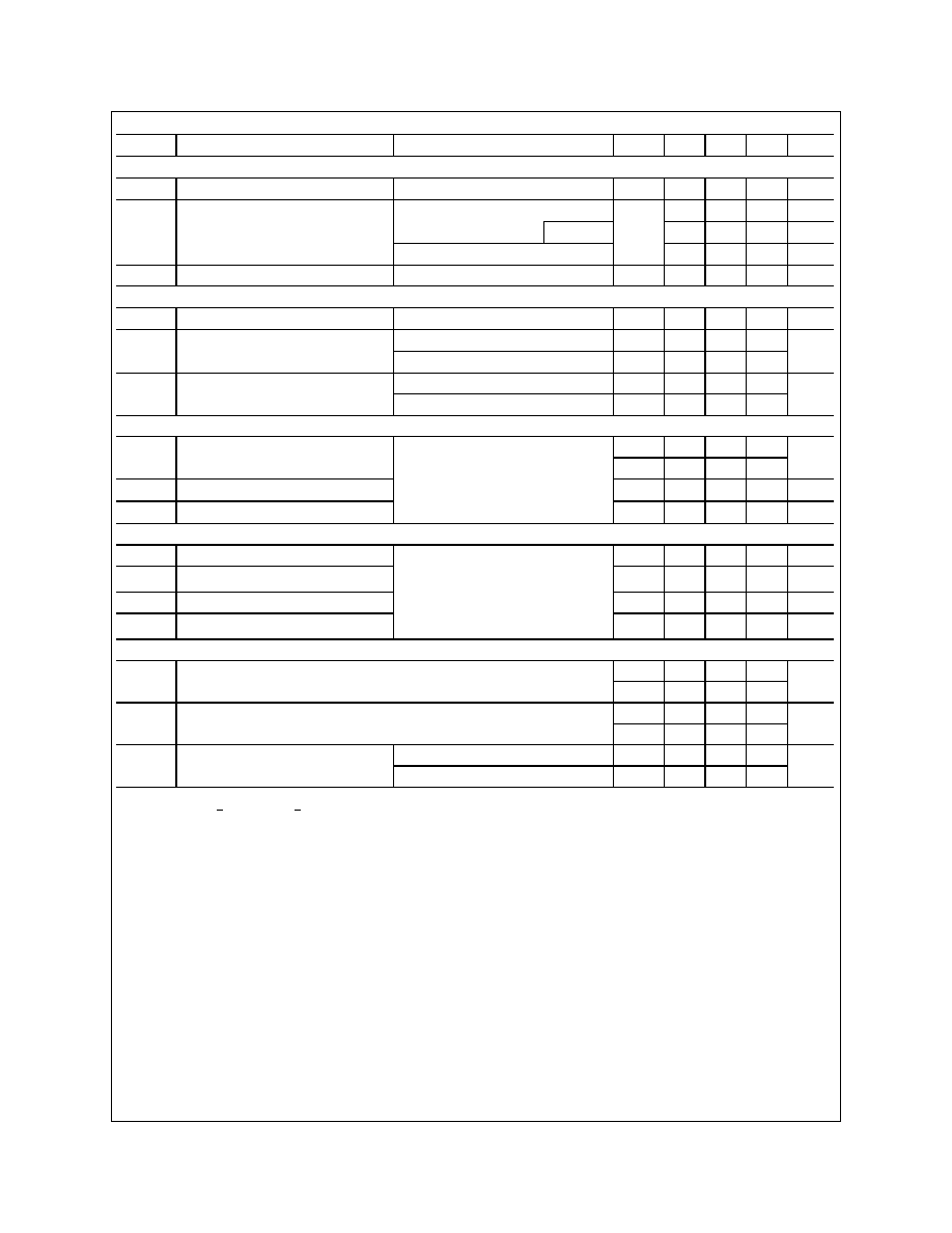
V , DRAIN-SOURCE VOLTAGE (V)
I , DRAIN-SOURCE CURRENT (A)
V = -10V
GS
DS
D
-8.0
-4.0
-6.0
-5.0
-4.5
-3.5
-2.5
-3.0
-1
-0.8
-0.6
-0.4
-0.2
0 .5
1
1 .5
2
2 .5
3
I , DRA IN CURRENT (A)
DRAIN-SOURCE ON-RESISTA
N
CE
V = -3V
GS
D
R , NORMALIZED
DS(on)
-3.5
-4.5
-5.0
-6 .0
-1 0
-4 .0
-8 .0
Figure 1. On-Region Characteristics
Figure 2. On-Resistance Variation
with Drain Current and Gate Voltage
Typical Electrical Characteristics
-50
-25
0
2 5
5 0
7 5
1 0 0
1 2 5
1 5 0
0 .6
0 .8
1
1 .2
1 .4
1 .6
T , JUNCTION TEMPERATURE (°C)
DRAIN-SOURCE ON-RESISTANCE
J
R ,
NORMALIZED
DS(ON)
I = -0.13A
V = -10V
D
GS
-1
-0.8
-0.6
-0.4
-0.2
0.5
1
1.5
2
2.5
3
I , DRAIN CURRENT (A)
DRAIN-SOURCE ON-RESISTANCE
T = 1 2 5 ° C
J
D
R ,
NORMALIZ
ED
DS(on)
25°C
-55°C
V = -10V
GS
Figure 3. On-Resistance Variation
with Temperature
Figure 4. On-Resistance Variation
with Drain Current and Temperature
-8
-6
-4
-2
0
-1
-0 .8
-0 .6
-0 .4
-0 .2
V , GATE TO SOURCE VOLTAGE (V)
I , DRAI
N
C
URRENT (A)
2 5 ° C
1 2 5 ° C
V = -10V
DS
GS
D
T = -55°C
J
-5 0
-25
0
2 5
5 0
7 5
1 0 0
1 2 5
1 5 0
0.85
0.9
0.95
1
1.05
1.1
T , JUNCTION TEM PERATURE (°C)
GAT
E-SO
URCE THRESHOLD VOLTAGE
J
V = V
I = -1m A
D
DS
GS
V , NOR
MALIZED
th
Figure 5. Transfer Characteristics
Figure 6. Gate Threshold Variation
with Temperature
BSS84 Rev. C1 / BSS110. Rev. A2
-50
-25
0
2 5
5 0
7 5
1 0 0
1 2 5
1 5 0
0 .9
0 .9 5
1
1 .0 5
1 .1
T , JUNCTION TEMPERATURE (°C)
DRAIN-SOURCE BREAKDO
WN VOLTAGE
I = - 2 5 0 µ A
D
BV , NOR
MALIZED
DSS
J
0.2
0.4
0.6
0.8
1
1.2
1.4
1.6
0.001
0.005
0.01
0.05
0.1
0.2
0.5
1
-V , BODY DIODE FORWARD VOLTAGE (V)
-I , REVERSE DRAIN C
URRENT (A)
V = 0 V
GS
T = 1 2 5 ° C
J
2 5 ° C
-55°C
SD
S
Figure 7. Breakdown Voltage
Variation with Temperature
Figure 8. Body Diode Forward Voltage
Variation with Source
Current and Temperature
Typical Electrical Characteristics
(continued)
0
0 .5
1
1 .5
2
0
2
4
6
8
1 0
Q , GATE CHARGE (nC)
-V , GATE-SOURCE VOLTAGE (V)
g
GS
V = -10V
DS
I = -0.13A
D
-20V
-40V
0 .1
0 .2
0 .5
1
2
5
1 0
2 0
3 0
5 0
2
3
5
1 0
2 0
3 0
5 0
7 0
-V , DRA IN TO SOURCE VOLTAGE (V)
CAPACITANCE (pF)
DS
C
iss
f = 1 M H z
V = 0V
GS
C
oss
C
rss
Figure 9. Capacitance Characteristics
Figure 10. Gate Charge Characteristics
G
D
S
V
DD
R
L
V
V
IN
OUT
V
GS
DUT
R
GEN
10%
50%
90%
10%
90%
90%
50%
V
IN
V
OUT
o n
off
d (off)
f
r
d (on)
t
t
t
t
t
t
INVERTED
10%
PULSE W IDTH
Figure 11. Switching Test Circuit
Figure 12. Switching Waveforms
BSS84 Rev. C1 / BSS110. Rev. A2
-1
-0.8
-0.6
-0.4
-0.2
0
0 .1
0 .2
0 .3
0 .4
0 .5
I , DRAIN CURRENT (A)
g
, TR
ANS
CONDUCTAN
CE (SIE
M
E
NS
)
T = -55°C
J
D
FS
V = -10V
DS
1 2 5 ° C
2 5 ° C
1
2
5
1 0
2 0
3 0
5 0
8 0
0 .005
0 .01
0 .05
0 .1
0 .5
1
2
- V , DRAIN -SOURCE VOLTAGE (V)
-I , DR
A
IN CURRENT (A)
DS
D
V = -10V
SINGLE PULSE
T = 2 5 ° C
GS
A
RDS(ON) Li
m
it
100
m s
1 m
s
10
m s
DC
1s
100us
10
s
Figure 13. Transconductance Variation with Drain
Current and Temperature
Figure 14. Maximum Safe Operating Area
Typical Electrical Characteristics
(continued)
0.0001
0.001
0.01
0.1
1
10
100
300
0.001
0.002
0.01
0.05
0.1
0.2
0.5
1
t , TIME (sec)
T
R
A
N
S
I
E
N
T
T
H
E
R
M
A
L
R
E
S
I
S
T
A
N
C
E
r(t), NORMALIZED EFFECTIVE
1
Single Pulse
D = 0.5
0 .1
0 .05
0 .02
0 .01
0 .2
Duty Cycle, D = t /t
1
2
R (t) = r (t) * R
R = 3 5 0 C/ W
JA
JA
JA
T - T = P * R (t)
JA
A
J
P(pk)
t
1
t
2
o
Figure 15. Transient Thermal Response Curve
Note : Characterization performed using a circuit board with 175
o
C/W
typical case-to-ambient thermal resistance
.