3
BSR18A
PNP General Purpose Amplifier
Absolute Maximum Ratings*
TA = 25°C unless otherwise noted
*
These ratings are limiting values above which the serviceability of any semiconductor device may be impaired.
Thermal Characteristics
TA = 25°C unless otherwise noted
This device is designed as a general purpose amplifier and
switching applications at collector currents of 10
µ
A to 100
mA. Sourced from Process 66.
Symbol
Parameter
Value
Units
V
CEO
Collector-Emitter Voltage
40
V
V
CBO
Collector-Base Voltage
40
V
V
EBO
Emitter-Base Voltage
5.0
V
I
C
Collector Current - Continuous
200
mA
T
J
, T
stg
Operating and Storage Junction Temperature Range
-55 to +150
°
C
Symbol
Characteristic
Max
Units
*BSR18A
P
D
Total Device Dissipation
Derate above 25
°
C
350
2.8
mW
mW/
°
C
R
JA
Thermal Resistance, Junction to Ambient
357
°
C/W
C
E
B
SOT-23
Mark: T92
*
Device mounted on FR-4 PCB 40 mm X 40 mm X 1.5 mm.
1997 Fairchild Semiconductor Corporation
NOTES:
1) These ratings are based on a maximum junction temperature of 150 degrees C.
2) These are steady state limits. The factory should be consulted on applications involving pulsed or low duty cycle operations.
3) All voltages (V) and currents (A) are negative polarity for PNP transistors.
BSR18A
BSR18A
Electrical Characteristics
TA = 25°C unless otherwise noted
OFF CHARACTERISTICS
Symbol
Parameter
Test Conditions
Min
Max
Units
V
(BR)CEO
Collector-Emitter Breakdown
Voltage
I
C
= 10
µ
A, I
B
= 0
40
V
V
(BR)CBO
Collector-Base Breakdown Voltage
I
C
= 1.0 mA, I
E
= 0
40
V
V
(BR)EBO
Emitter-Base Breakdown Voltage
I
E
= 10
µ
A, I
C
= 0
5.0
V
I
CBO
Collector-Cutoff Current
V
CB
= 30 V
50
nA
I
EBO
Emitter-Cutoff Current
V
EB
= 3.0 V, I
C
= 0
50
nA
ON CHARACTERISTICS*
h
FE
DC Current Gain
I
C
= 0.1 mA, V
CE
= 1.0 V
I
C
= 1.0 mA, V
CE
= 1.0 V
I
C
= 10 mA, V
CE
= 1.0 V
I
C
= 50 mA, V
CE
= 1.0 V
I
C
= 100 mA, V
CE
= 1.0 V
60
80
100
60
30
300
V
CE(
sat
)
Collector-Emitter Saturation Voltage
I
C
= 10 mA, I
B
= 1.0 mA
I
C
= 50 mA, I
B
= 5.0 mA
0.25
0.4
V
V
V
BE(
sat
)
Base-Emitter Saturation Voltage
I
C
= 10 mA, I
B
= 1.0 mA
I
C
= 50 mA, I
B
= 5.0 mA
0.65
0.85
0.95
V
V
SMALL SIGNAL CHARACTERISTICS
f
T
Transition Frequency
I
C
= 10 mA, V
CE
= 20,
f = 100 MHz
250
MHz
C
cb
Collector-Base Capacitance
V
CB
= 5.0 V, I
E
= 0, f = 100 kHz
4.5
pF
C
eb
Emitter-Base Capacitance
V
EB
= 0.5 V, I
C
= 0, f = 100 kHz
10
pF
h
ie
Input Impedance
V
CE
= 10 V,I
C
= 1.0 mA,f=1.0 kHz
2.0
12
k
h
fe
Small-Signal Current Gain
V
CE
= 10 V,I
C
= 1.0 mA,f=1.0 kHz
100
400
h
oe
Output Admittance
V
CE
= 10 V,I
C
= 1.0 mA,f=1.0 kHz
3.0
60
µ
S
SWITCHING CHARACTERISTICS
t
d
Delay Time
I
C
= 10 mA, I
B1
= 1.0 mA,
35
ns
t
r
Rise Time
V
EB
= 0.5 V
35
ns
t
s
Storage Time
I
C
= 10 mA, I
B
on
= I
B
off
= 1.0 mA
275
ns
t
f
Fall Time
75
ns
*
Pulse Test: Pulse Width
300
µ
s, Duty Cycle
0.01%
Spice Model
PNP (Is=1.41f Xti=3 Eg=1.11 Vaf=18.7 Bf=180.7 Ne=1.5 Ise=0 Ikf=80m Xtb=1.5 Br=4.977 Nc=2 Isc=0 Ikr=0
Rc=2.5 Cjc=9.728p Mjc=.5776 Vjc=.75 Fc=.5 Cje=8.063p Mje=.3677 Vje=.75 Tr=33.42n Tf=179.3p Itf=.4 Vtf=4
Xtf=6 Rb=10)
PNP General Purpose Amplifier
(continued)
NOTE: All voltages (V) and currents (A) are negative polarity for PNP transistors.
3
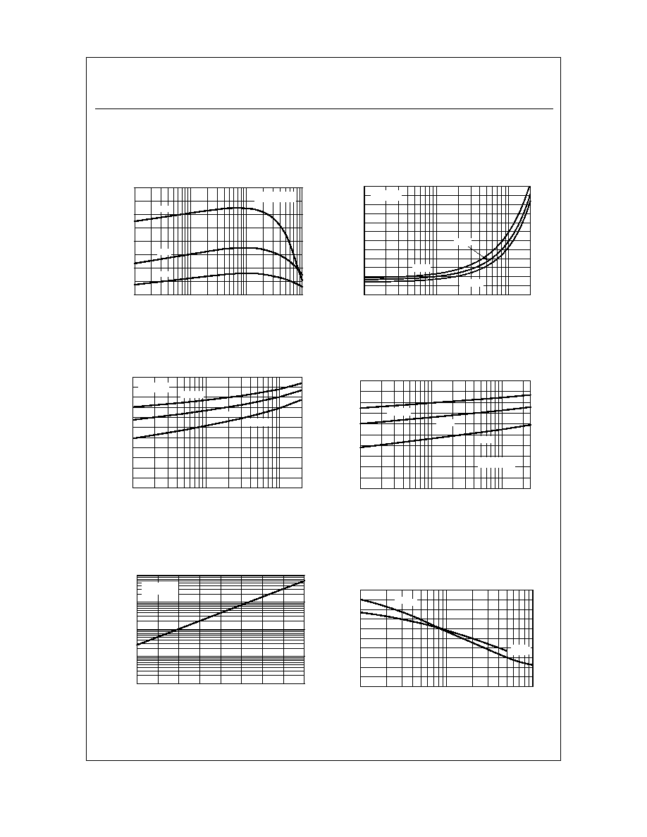
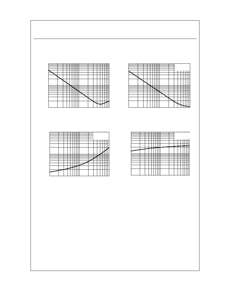
Typical Characteristics
Common-Base Open Circuit
Input and Output Capacitance
vs Reverse Bias Voltage
0.1
1
10
0
2
4
6
8
10
REVERSE BIAS VOLTAGE (V)
CA
P
A
CI
T
A
NCE (
p
F
)
C obo
C ibo
Ty pical Pulsed Current Gain
v s Collector Current
0.1
0.2
0.5
1
2
5
10
20
50
100
50
100
150
200
250
I - COLLECTOR CURRE NT (mA)
h
-
T
YPI
C
A
L
P
U
L
SED
C
U
R
R
EN
T
G
A
I
N
C
FE
125 °C
25 °C
- 40 °C
V = 1 .0V
CE
Collector-Emitter Saturation
Voltage vs Collector Current
1
10
100
200
0
0.05
0.1
0.15
0.2
0.25
0.3
I - COLLECTOR CURRE NT (mA)
V
-
C
O
L
L
E
C
T
O
R
E
M
IT
T
E
R
V
O
L
T
A
G
E
(
V
)
C
CE
S
A
T
25 °C
- 40 °C
125°C
= 10
Base-Emitter Saturation
Voltage vs Collector Current
1
10
100
200
0
0.2
0.4
0.6
0.8
1
I - COLLECTOR CURRE NT (mA)
V
-
B
A
S
E
E
M
IT
T
E
R
V
O
L
T
A
G
E
(
V
)
C
BE
S
A
T
= 10
25 °C
- 40 °C
125 °C
Base Emitter ON Voltage vs
Collector Current
0.1
1
10
25
0
0.2
0.4
0.6
0.8
1
I - COLLECTOR CURRE NT (mA)
V
-
B
A
S
E
E
M
IT
T
E
R
O
N
V
O
L
T
A
G
E
(
V
)
C
BE
(
O
N
)
V = 1V
CE
25 °C
- 40 °C
125 °C
Collector-Cutoff Current
vs Ambient Temperature
25
50
75
100
125
0.01
0.1
1
10
100
T - AMBIE NT TEMP ERATURE ( C)
I
-
C
O
L
L
E
C
T
O
R
CU
RR
E
N
T
(
n
A)
A
CBO
°
V = 25V
CB
BSR18A
PNP General Purpose Amplifier
(continued)
BSR18A
Power Dissipation vs
Ambient Temperature
0
25
50
75
100
125
150
0
50
100
150
200
250
300
350
TEMPERATURE ( C)
P
- P
O
W
E
R
D
I
SS
IP
A
T
IO
N
(mW
)
D
o
SOT-23
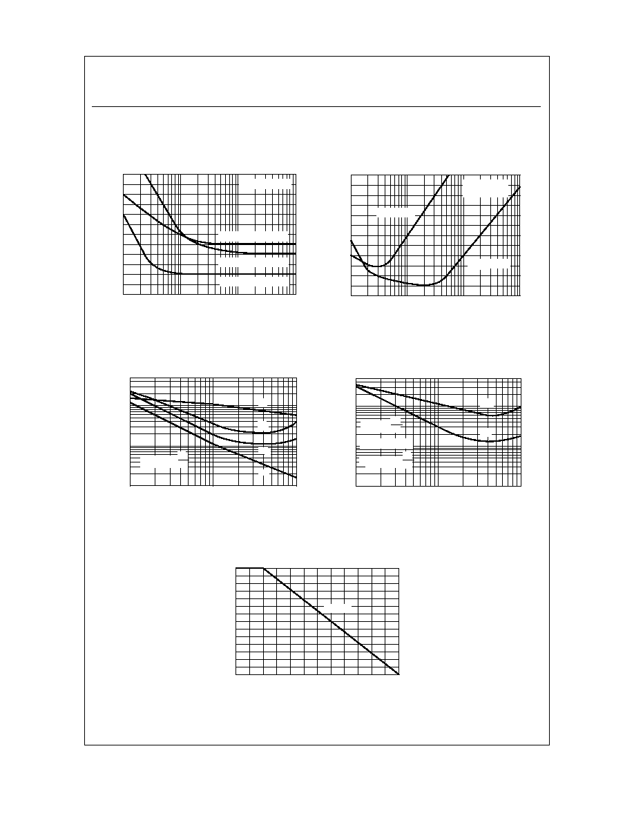
Typical Characteristics
(continued)
PNP General Purpose Amplifier
(continued)
Noise Figure vs Frequency
0.1
1
10
100
0
1
2
3
4
5
6
f - FREQUENCY (kHz)
NF
-
NO
I
S
E
F
I
GU
RE
(
d
B
)
I = 100
µ
A, R = 200
C
V = 5.0V
CE
S
I = 100
µ
A, R = 2.0 k
C
S
I = 1.0 mA, R = 200
C
S
Noise Figure vs Source Resistance
0.1
1
10
100
0
2
4
6
8
10
12
R - SOURCE RESISTANCE ( )
NF
-
NO
I
S
E
F
I
G
U
RE
(
d
B)
k
I = 100
µ
A
C
V = 5.0V
f = 1.0 kHz
CE
I = 1.0 mA
C
S
Switching Times
vs Collector Current
1
10
100
1
10
100
500
I - COLLECTOR CURRENT (mA)
T
I
ME
(n
S
)
I = I =
t r
t
s
B1
C
B2
I
c
10
t f
t d
Turn On and Turn Off Times
vs Collector Current
1
10
100
1
10
100
500
I - COLLECTOR CURRENT (mA)
TI
M
E
(
n
S
)
I = I =
t
off
B1
B2
I
c
10
t
on
V = 0.5V
BE(OFF)
t
I =
on
t
off
B1
I
c
10
3
Typical Characteristics
(continued)
Input Impedance
0.1
1
10
0.1
1
10
I - COLLECTOR CURRENT (mA)
h
-
I
N
PU
T I
M
PED
ANC
E
(
k
)
V = 10 V
CE
C
ie
f = 1.0 kHz
Output Admittance
0.1
1
10
10
100
1000
I - COLLECTOR CURRENT (mA)
h
-
O
U
TPU
T
A
D
M
I
T
T
A
N
C
E
(
m
h
o
s
)
V = 10 V
CE
C
oe
f = 1.0 kHz
µ
Current Gain
0.1
1
10
10
20
50
100
200
500
1000
I - COLLECTOR CURRENT (mA)
h
-
C
U
R
R
E
N
T G
A
I
N
V = 10 V
CE
C
fe
f = 1.0 kHz
Voltage Feedback Ratio
0.1
1
10
1
10
100
I - COLLECTOR CURRENT (mA)
h
-
V
O
L
T
A
G
E
F
E
E
D
B
A
C
K
R
A
T
IO
(
x
1
0
)
C
re
_
4
BSR18A
PNP General Purpose Amplifier
(continued)