RFMA0912-1W-SMP
ISSUED
06/30/2005
9.5 11.7 GHz Power AMPLIFIER MMIC
Specifications are subject to change without notice.
Excelics Semiconductor, Inc. 310 De Guigne Drive, Sunnyvale, CA 94085
page 1 of 3
Phone: 408-737-1711 Fax: 408-737-1868 Web:
www.excelics.com
Revised July 2005
FEATURES
·
9.5 11.7GHz Operating Frequency Range
·
30dBm Output Power at 1dB Compression
·
32 dB Typical Small Signal Gain
·
-41dBc OIMD3 @Each Tone Pout 19dBm
·
Small Surface Mount Package
APPLICATIONS
·
Point-to-point and point-to-multipoint radio
·
Military Radar Systems
1
2
3
4
5
6
7
8
9
10
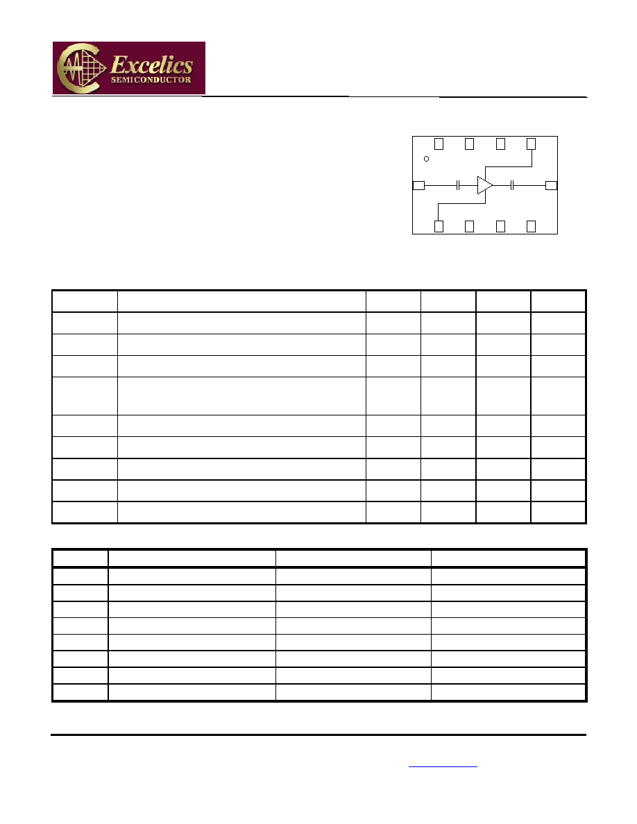
IN
OUT
VD
VG
ELECTRICAL CHARACTERISTICS (T
a
= 25
°
C, V
DD
=7V, Idsq=900mA)
SYMBOL PARAMETER/TEST
CONDITIONS MIN
TYP
MAX
UNITS
F
Operating Frequency Range
9.5
11.7
GHz
P
1dB
Output Power at 1dB Gain Compression
29
30
dBm
Gss
Small Signal Gain
29
32
dB
OIMD3
Output 3
rd
Order Intermodulation Distortion
@f=10MHz, Each Tone Pout 19dBm
V
DD
=7V, Idsq=60%±10%Idss
-41 -38 dBc
Input RL
Input Return Loss
-10
-8
dB
Output RL
Output Return Loss
-6
dB
Idss
Saturated Drain Current
1120
1400
1680
mA
V
DD
Drain Voltage
7
8
V
Rth
Thermal Resistance
11
o
C/W
MAXIMUM RATINGS AT 25°C
1,2
SYMBOL CHARACTERISTIC
ABSOLUTE
CONTINOUS
V
DS
Drain to Source Voltage
12V
8 V
V
GS
Gate to Source Voltage
-8V
-3 V
I
DD
Drain
Current
Idss
1.9A
I
GSF
Forward Gate Current
132mA
22mA
P
IN
Input Power
20dBm
@ 3dB compression
T
CH
Channel
Temperature
175°C
150°C
T
STG
Storage
Temperature
-65/175°C
-65/150°C
P
T
Total
Power
Dissipation
15.0W
12.6W
1. Operating the device beyond any of the above rating may result in permanent damage.
2. Bias conditions must also satisfy the following equation V
DS
*I
DS
< (T
CH
T
HS
)/R
TH
; where T
HS
= Base Plate Temperature
RFMA0912-1W-SMP
ISSUED
06/30/2005
9.5 11.7 GHz Power AMPLIFIER MMIC
Specifications are subject to change without notice.
Excelics Semiconductor, Inc. 310 De Guigne Drive, Sunnyvale, CA 94085
page 2 of 3
Phone: 408-737-1711 Fax: 408-737-1868 Web:
www.excelics.com
Revised July 2005
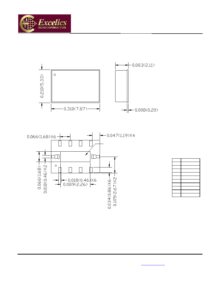
Package Dimension and Pin Assignment
Ground Plane
1
2
3
10
5
S M P
BOTTOM SIDE VIEW
10
0 9 1 2 _ 1 W
R F M A
5
TOP SIDE VIEW
1
2
3
4
6
7
8
9
4
6
7
8
9
EXCELICS
NOTES:
1. Material:
Plastic
2.
Plating: Gold over Nickel
3.
Ground Plane Must be Soldered to PCB RF Ground.
4.
°
Indicates PIN 1.
5.
All Dimensions are in Inches (Millimeters).
6.
All Tolerances are ±0.003 (±0.08).
PIN Assignment
1 N/C
2 N/C
3 N/C
4 VD
5 OUT
6 N/C
7 N/C
8 N/C
9 VG
10 IN
RFMA0912-1W-SMP
ISSUED
06/30/2005
9.5 11.7 GHz Power AMPLIFIER MMIC
Specifications are subject to change without notice.
Excelics Semiconductor, Inc. 310 De Guigne Drive, Sunnyvale, CA 94085
page 3 of 3
Phone: 408-737-1711 Fax: 408-737-1868 Web:
www.excelics.com
Revised July 2005
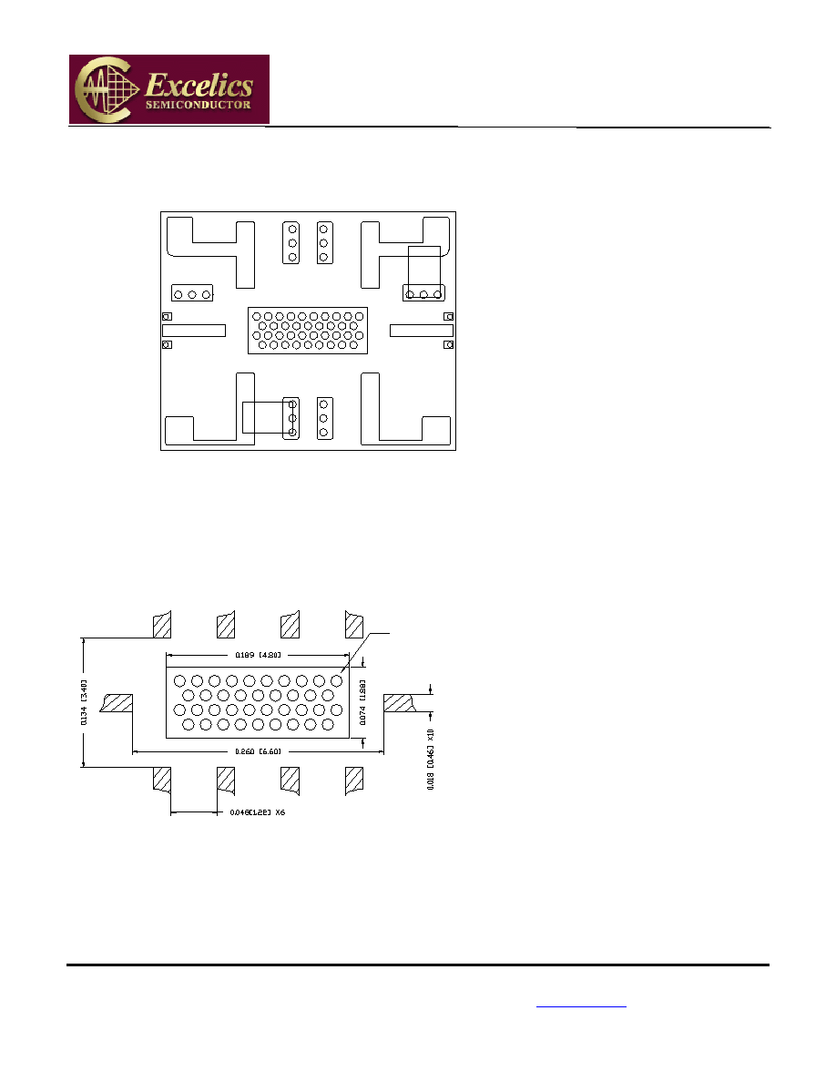
Evaluation Board
0.1uF
Cap
0.1uF
Cap
1
4
5
6
9
10
Suggested PCB Land Pattern
Suggested Ground Plane
Via Size Ř0.008[0.20]
Via Center to Center 0.018[0.45]
Notes:
1.
All Dimensions Are
In Inches
[Millimeters]
2.
All Tolerances Are
±0.003[0.08]
3. Suggested
PCB
Material Is
Rogers4003 with
1/2oz Copper
4. Suggested
PCB
Thickness is 8mil
The grounded Co-Planar Wave
Guide (CPWG) PCB
input/output transitions allow
use of Ground_Signal_Ground
(GSG) probes for testing.
Suggested probe pitch is
500um. Alternatively, the
evaluation board can be
mounted in a metal housing
with SMA coaxial connectors.