
Exar
Corporation 48720 Kato Road, Fremont CA, 94538
·
(510) 668-7000
·
FAX (510) 668-7017
·
www.exar.com
áç
áç
áç
áç
XRT75L02
TWO CHANNEL E3/DS3/STS-1 LINE INTERFACE UNIT WITH JITTER
NOVEMBER 2003
REV. 1.0.1
GENERAL DESCRIPTION
The XRT75L02 is a two-channel fully integrated Line
Interface Unit (LIU) with Jitter Attenuator for E3/DS3/
STS-1 applications. It incorporates independent
Receivers, Transmitters and Jitter Attenuators in a
single 100 pin TQFP package.
The XRT75L02 can be configured to operate in either
E3 (34.368 MHz), DS3 (44.736 MHz) or STS-1 (51.84
MHz) modes.The transmitter can be turned off (tri-
stated) for redundancy support and for conserving
power.
The XRT75L02's differential receiver provides high
noise interference margin and is able to receive the
data over 1000 feet of cable or with up to 12 dB of
cable attenuation.
The XRT75L02 incorporates advanced crystal-less
jitter attenuators that can be selected either in the
transmit or receive path. The jitter attenuator
performance meets the ETSI TBR-24 and Bellcore
GR-499 specifications.
The XRT75L02 provides both Serial Microprocessor
Interface as well as Hardware mode for programming
and control.
The XRT75L02 supports local,remote and digital
loop-backs. The XRT75L02 also contains an on-
board Pseudo Random Binary Sequence (PRBS)
generator and detector with the ability to insert and
detect single bit error.
FEATURES
RECEIVER:
·
On chip Clock and Data Recovery circuit for high
input jitter tolerance.
·
Meets the jitter tolerance requirements as specified
in ITU-T G.823_1993 for E3 and Telcordia GR-499-
CORE for DS3 applications.
·
Detects and Clears LOS as per G.775.
·
Receiver Monitor mode handles up to 20 dB flat
loss with 6 dB cable attenuation.
·
On chip B3ZS/HDB3 encoder and decoder that can
either be enabled or disabled.
·
On-chip clock synthesizer generates the
appropriate rate clock from a single frequency
XTAL.
·
Provides low jitter clock outputs for either DS3,E3
or STS-1 rates.
·
On-chip clock synthesizer provides the appropriate
rate clock from a single 12.288 MHz Clock.
·
Provides low jitter output clock.
TRANSMITTER:
·
Compliant with Bellcore GR-499, GR-253 and ANSI
T1.102 Specification for transmit pulse
·
Tri-state Transmit output capability for redundancy
applications
·
Transmitters can be turned on or off.
JITTER ATTENUATOR:
·
On chip advanced crystal-less Jitter Attenuator.
·
Jitter Attenuator can be selected in Receive or
Transmit paths.
·
16 or 32 bits selectable FIFO size.
·
Meets the Jitter and Wander specifications
described in T1.105.03b,ETSI TBR-24, Bellcore
GR-253 and GR-499 standards.
·
Jitter Attenuators can be disabled.
CONTROL AND DIAGNOSTICS:
·
5 wire Serial Microprocessor Interface for control
and configuration.
·
Supports optional internal Transmit Driver
Monitoring.
·
PRBS error counter register to accumulate errors.
·
Hardware Mode for control and configuration.
·
Supports Local, Remote and Digital Loop-backs.
·
Single 3.3 V ± 5% power supply.
·
5 V Tolerant I/O.
·
Available in 100 pin TQFP.
·
-40°C to 85°C Industrial Temperature Range.
APPLICATIONS
·
E3/DS3 Access Equipment.
·
STS1-SPE to DS3 Mapper.
·
DSLAMs.
·
Digital Cross Connect Systems.
·
CSU/DSU Equipment.
·
Routers.
·
Fiber Optic Terminals.

XRT75L02
áç
áç
áç
áç
TWO CHANNEL E3/DS3/STS-1 LINE INTERFACE UNIT WITH JITTER
REV. 1.0.1
2
TRANSMIT INTERFACE CHARACTERISTICS
·
Accepts either Single-Rail or Dual-Rail data from Terminal Equipment and generates a bipolar signal to the
line
·
Integrated Pulse Shaping Circuit.
·
Built-in B3ZS/HDB3 Encoder (which can be disabled).
·
Accepts Transmit Clock with duty cycle of 30%-70%.
·
Generates pulses that comply with the ITU-T G.703 pulse template for E3 applications.
·
Generates pulses that comply with the DSX-3 pulse template, as specified in Bellcore GR-499
-CORE
and
ANSI T1.102_1993.
·
Generates pulses that comply with the STSX-1 pulse template, as specified in Bellcore GR-253-CORE.
·
Transmitter can be turned off in order to support redundancy designs.
RECEIVE INTERFACE CHARACTERISTICS
·
Integrated Adaptive Receive Equalization for optimal Clock and Data Recovery.
·
Declares and Clears the LOS defect per ITU-T G.775 requirements for E3 and DS3 applications.
·
Meets Jitter Tolerance Requirements, as specified in ITU-T G.823_1993 for E3 Applications.
·
Meets Jitter Tolerance Requirements, as specified in Bellcore GR-499-CORE for DS3 Applications.
·
Declares Loss of Signal (LOS) and Loss of Lock (LOL) Alarms.
·
Built-in B3ZS/HDB3 Decoder (which can be disabled).
F
IGURE
1. B
LOCK
D
IAGRAM
OF
THE
XRT 75L02
HOST/HW
STS-1/DS3
E3
REQEN
RTIP
RRING
SR/DR
XRT75L03
RLB
RLOS
JATx/Rx
TPOS
TNEG
TxClk
TAOS
TxLEV
TxON
Note: Serial Processor Interface input pins are shared by in "Host" Mode and redefined in the "Hardware" Mode.
Device
Monitor
MTIP
MRING
DMO
Timing
Control
TTIP
TRING
Tx
Pulse
Shaping
HDB3/
B3ZS
Encoder
RLOL
RxON
RxClkINV
RxClk
RPOS
RNEG/
LCV
Tx
Control
Jitter
Attenuator
MUX
Line
Driver
LLB
Invert
Remote
LoopBack
HDB3/
B3ZS
Decoder
MUX
AGC/
Equalizer
Peak Detector
LOS
Detector
Slicer
Jitter
Attenuator
Serial
Processor
Interface
Local
LoopBack
Clock & Data
Recovery
Clock
Synthesizer
E3Clk,DS3Clk,
STS-1Clk
RESET
CS
SClk
INT
SDO
SDI
CLK_OUT
áç
áç
áç
áç
XRT75L02
REV. 1.0.1
TWO CHANNEL E3/DS3/STS-1 LINE INTERFACE UNIT WITH JITTER
3
·
Recovered Data can be muted while the LOS Condition is declared.
·
Outputs either Single-Rail or Dual-Rail data to the Terminal Equipment.
F
IGURE
2. P
IN
O
UT
OF
THE
XRT75L02
ORDERING INFORMATION
P
ART
N
UMBER
P
ACKAGE
O
PERATING
T
EMPERATURE
R
ANGE
XRT75L02IV
14mm x 14mm 100 Pin TQFP
-40
°
C to +85
°
C
XRT75L02
1
2
3
4
5
6
7
8
9
10
11
12
13
14
15
16
17
18
19
20
21
22
23
24
25
75
74
73
72
71
70
69
68
67
66
65
64
63
62
61
60
59
58
57
56
55
54
53
52
51
50
49
48
47
46
45
44
43
42
41
40
39
38
37
36
35
34
33
32
31
30
29
28
27
26
76
77
78
79
80
81
82
83
84
85
86
87
88
89
90
91
92
93
94
95
96
97
98
99
100
TA
O
S
_
0
T
x
L
EV_
0
MR
I
N
G
_
0
MT
I
P
_
0
TR
I
N
G
_
0
TT
I
P
_
0
T
x
DV
DD_0
T
x
DG
ND_
0
DV
DD
E3
C
L
K
DG
N
D
DG
N
D
DS
3CL
K
DV
DD
DV
DD
ST
S1
C
L
K/
SF
M
C
L
K
DG
N
D
T
x
DG
ND_
1
T
x
DV
DD_1
TT
I
P
_
1
TR
I
N
G
_
1
MT
I
P
_
1
MR
I
N
G
_
1
T
x
L
EV_
1
TA
O
S
_
1
RE
Q
E
N_0
E3
_
0
ST
S1
/
D
S3
_
0
LL
B
_
0
RLB
_
0
Rx
A
V
D
D_
0
Rx
A
G
ND
_
0
RR
I
N
G
_
0
RT
I
P
_
0
AG
N
D
Rx
A
Rx
B
AVD
D
JA_
0
JA_
1
JAT
x
/
R
x
RT
I
P
_
1
RR
I
N
G
_
1
Rx
A
G
ND
_
1
Rx
A
V
D
D_
1
RLB
_
1
LL
B
_
1
ST
S1
/
D
S3
_
1
E3
_
1
RE
Q
E
N_1
TNEG_1
TPOS_1
TxCLK_1
DMO_1
CLKOUT_1
CLKOUT_EN
TxAGND_1
TxAVDD_1
JAAGND_1
JAAVDD_1
JADVDD_1
JADGND_1
DVDD_1
DGND_1
RxCLK_1
RPOS_1
RNEG/LCV_1
RLOS_1
RLOL_1
SDI/RxON
SCLK/TxCLKINV
CS/RxCLKINV
INT/LOSMUT
SDO/RxMON
HOST/HW
TNEG_0
TPOS_0
TxCLK_0
DMO_0
CLKOUT_0
TxON
TxMON
TxAGND_0
TxAVDD_0
JAAGND_0
JAAVDD_0
JADVDD_0
JADGND_0
RxDVDD_0
RxDGND_0
RxCLK_0
RPOS_0
RNEG/LCV_0
RLOS_0
RLOL_0
TEST
RESET
ICT
SFM_EN
SR/DR

XRT75L02
áç
áç
áç
áç
REV. 1.0.1
TWO CHANNEL E3/DS3/STS-1 LINE INTERFACE UNIT WITH JITTER
I
TABLE OF CONTENTS
GENERAL DESCRIPTION .................................................................................................1
F
EATURES
.....................................................................................................................................................1
A
PPLICATIONS
................................................................................................................................................1
T
RANSMIT
I
NTERFACE
C
HARACTERISTICS
........................................................................................................2
R
ECEIVE
I
NTERFACE
C
HARACTERISTICS
..........................................................................................................2
F
IGURE
1. B
LOCK
D
IAGRAM
OF
THE
XRT 75L02 .............................................................................................................................. 2
F
IGURE
2. P
IN
O
UT
OF
THE
XRT75L02............................................................................................................................................ 3
ORDERING INFORMATION .....................................................................................................................3
PIN DESCRIPTIONS (BY FUNCTION) .............................................................................4
T
RANSMIT
I
NTERFACE
.....................................................................................................................................4
R
ECEIVE
I
NTERFACE
.......................................................................................................................................6
C
LOCK
I
NTERFACE
.........................................................................................................................................8
CONTROL AND ALARM INTERFACE ........................................................................................................9
M
ODE
S
ELECT
............................................................................................................................................11
M
ICROPROCESSOR
S
ERIAL
INTERFACE - (HOST MODE) .........................................................................11
...................................................................................................................................................................12
J
ITTER
A
TTENUATOR
INTERFACE
...................................................................................................................12
A
NALOG
P
OWER
AND
G
ROUND
.....................................................................................................................13
DIGITAL
P
OWER
AND
G
ROUND
......................................................................................................................13
1.0 ELECTRICAL CHARACTERISTICS ....................................................................................................15
T
ABLE
1: A
BSOLUTE
M
AXIMUM
R
ATINGS
......................................................................................................................................... 15
T
ABLE
2: DC E
LECTRICAL
C
HARACTERISTICS
: ................................................................................................................................ 15
2.0 TIMING CHARACTERISTICS ..............................................................................................................16
F
IGURE
3. T
YPICAL
INTERFACE
BETWEEN
TERMINAL
EQUIPMENT
AND
THE
XRT75L02 (
DUAL
-
RAIL
DATA
)........................................... 16
F
IGURE
4. T
RANSMITTER
T
ERMINAL
I
NPUT
T
IMING
.......................................................................................................................... 16
F
IGURE
5. R
ECEIVER
D
ATA
OUTPUT
AND
CODE
VIOLATION
TIMING
................................................................................................... 17
F
IGURE
6. T
RANSMIT
I
NTERFACE
CIRCUIT
FOR
E3, DS3
AND
STS-1 R
ATES
.................................................................................... 17
3.0 LINE SIDE CHARACTERISTICS: ........................................................................................................18
3.1 E3 LINE SIDE PARAMETERS: ...................................................................................................................... 18
F
IGURE
7. P
ULSE
M
ASK
FOR
E3 (34.368
MBITS
/
S
)
INTERFACE
AS
PER
ITU
-
T
G.703 ......................................................................... 18
T
ABLE
3: E3 T
RANSMITTER
LINE
SIDE
OUTPUT
AND
RECEIVER
LINE
SIDE
INPUT
SPECIFICATIONS
........................................................ 18
F
IGURE
8. B
ELLCORE
GR-253 CORE T
RANSMIT
O
UTPUT
P
ULSE
T
EMPLATE
FOR
SONET STS-1 A
PPLICATIONS
............................. 19
T
ABLE
4: STS-1 P
ULSE
M
ASK
E
QUATIONS
..................................................................................................................................... 19
T
ABLE
5: STS-1 T
RANSMITTER
L
INE
S
IDE
O
UTPUT
AND
R
ECEIVER
L
INE
S
IDE
I
NPUT
S
PECIFICATIONS
(GR-253) .............................. 20
F
IGURE
9. T
RANSMIT
O
UPUT
P
ULSE
T
EMPLATE
FOR
DS3
AS
PER
B
ELLCORE
GR-499 ..................................................................... 20
T
ABLE
6: DS3 P
ULSE
M
ASK
E
QUATIONS
........................................................................................................................................ 21
T
ABLE
7: DS3 T
RANSMITTER
L
INE
S
IDE
O
UTPUT
AND
R
ECEIVER
L
INE
S
IDE
I
NPUT
S
PECIFICATIONS
(GR-499) ................................. 21
F
IGURE
10. M
ICROPROCESSOR
S
ERIAL
I
NTERFACE
S
TRUCTURE
...................................................................................................... 22
F
IGURE
11. T
IMING
D
IAGRAM
FOR
THE
M
ICROPROCESSOR
S
ERIAL
I
NTERFACE
................................................................................ 22
T
ABLE
8: M
ICROPROCESSOR
S
ERIAL
I
NTERFACE
T
IMINGS
( TA = 250C, VDD=3.3V± 5%
AND
LOAD
= 10
P
F) .................................. 23
4.0 THE TRANSMITTER SECTION: ..........................................................................................................24
4.1 TRANSMIT CLOCK: ....................................................................................................................................... 24
4.2 B3ZS/HDB3 ENCODER: ................................................................................................................................. 24
4.2.1 B3ZS ENCODING: ...................................................................................................................................................... 24
F
IGURE
12. S
INGLE
-R
AIL
OR
NRZ D
ATA
F
ORMAT
(E
NCODER
AND
D
ECODER
ARE
E
NABLED
)............................................................ 24
F
IGURE
13. D
UAL
-R
AIL
D
ATA
F
ORMAT
(
ENCODER
AND
DECODER
ARE
DISABLED
) ............................................................................. 24
4.2.2 HDB3 ENCODING:...................................................................................................................................................... 25
4.3 TRANSMIT PULSE SHAPER: ........................................................................................................................ 25
F
IGURE
14. B3ZS E
NCODING
F
ORMAT
........................................................................................................................................... 25
F
IGURE
15. HDB3 E
NCODING
F
ORMAT
.......................................................................................................................................... 25
4.3.1 GUIDELINES FOR USING TRANSMIT BUILD OUT CIRCUIT: ................................................................................. 26
4.3.2 INTERFACING TO THE LINE: .................................................................................................................................... 26
4.4 TRANSMIT DRIVE MONITOR: ....................................................................................................................... 26
F
IGURE
16. T
RANSMIT
D
RIVER
M
ONITOR
SET
-
UP
. ........................................................................................................................... 26
4.5 TRANSMITTER SECTION ON/OFF: .............................................................................................................. 27
5.0 THE RECEIVER SECTION: .................................................................................................................27
5.1 AGC/EQUALIZER: .......................................................................................................................................... 27
5.1.1 INTERFERENCE TOLERANCE: ................................................................................................................................ 27

áç
áç
áç
áç
XRT75L02
TWO CHANNEL E3/DS3/STS-1 LINE INTERFACE UNIT WITH JITTER
REV. 1.0.1
II
5.2 CLOCK AND DATA RECOVERY: .................................................................................................................. 28
F
IGURE
17. I
NTERFERENCE
M
ARGIN
T
EST
S
ET
UP
FOR
DS3/STS-1................................................................................................ 28
F
IGURE
18. I
NTERFERENCE
M
ARGIN
T
EST
S
ET
UP
FOR
E3. ............................................................................................................ 28
T
ABLE
9: I
NTERFERENCE
M
ARGIN
T
EST
R
ESULTS
........................................................................................................................... 28
5.3 B3ZS/HDB3 DECODER: ................................................................................................................................ 29
5.4 LOS (LOSS OF SIGNAL) DETECTOR: ......................................................................................................... 29
5.4.1 DS3/STS-1 LOS CONDITION: .................................................................................................................................... 29
D
ISABLING
ALOS/DLOS D
ETECTION
: .......................................................................................................... 29
5.4.2 E3 LOS CONDITION:.................................................................................................................................................. 29
T
ABLE
10: T
HE
ALOS (A
NALOG
LOS) D
ECLARATION
AND
C
LEARANCE
T
HRESHOLDS
FOR
A
GIVEN
SETTING
OF
REQEN (DS3
AND
STS-1
A
PPLICATIONS
) ............................................................................................................................................................... 29
5.4.3 MUTING THE RECOVERED DATA WITH LOS CONDITION:................................................................................... 30
F
IGURE
19. L
OSS
O
F
S
IGNAL
D
EFINITION
FOR
E3
AS
PER
ITU-T G.775.......................................................................................... 30
F
IGURE
20. L
OSS
OF
S
IGNAL
D
EFINITION
FOR
E3
AS
PER
ITU-T G.775. ......................................................................................... 30
6.0 JITTER: ................................................................................................................................................ 31
6.1 JITTER TOLERANCE - RECEIVER: .............................................................................................................. 31
6.1.1 DS3/STS-1 JITTER TOLERANCE REQUIREMENTS:............................................................................................... 31
F
IGURE
21. J
ITTER
T
OLERANCE
M
EASUREMENTS
........................................................................................................................... 31
6.1.2 E3 JITTER TOLERANCE REQUIREMENTS:............................................................................................................. 32
F
IGURE
22. I
NPUT
J
ITTER
T
OLERANCE
F
OR
DS3/STS-1................................................................................................................ 32
F
IGURE
23. I
NPUT
J
ITTER
T
OLERANCE
FOR
E3 .............................................................................................................................. 32
6.2 JITTER TRANSFER - RECEIVER/TRANSMITTER: ...................................................................................... 33
6.3 JITTER GENERATION: .................................................................................................................................. 33
6.4 JITTER ATTENUATOR: ................................................................................................................................. 33
T
ABLE
11: J
ITTER
A
MPLITUDE
VERSUS
M
ODULATION
F
REQUENCY
(J
ITTER
T
OLERANCE
) .................................................................. 33
T
ABLE
12: J
ITTER
T
RANSFER
S
PECIFICATION
/R
EFERENCES
............................................................................................................ 33
T
ABLE
13: J
ITTER
T
RANSFER
P
ASS
M
ASKS
.................................................................................................................................... 34
F
IGURE
24. J
ITTER
T
RANSFER
R
EQUIREMENTS
AND
J
ITTER
A
TTENUATOR
P
ERFORMANCE
................................................................ 34
7.0 SERIAL HOST INTERFACE: ............................................................................................................... 35
T
ABLE
14: F
UNCTIONS
OF
SHARED
PINS
......................................................................................................................................... 35
T
ABLE
15: R
EGISTER
M
AP
AND
B
IT
N
AMES
.................................................................................................................................... 35
T
ABLE
16: R
EGISTER
M
AP
D
ESCRIPTION
- G
LOBAL
......................................................................................................................... 36
T
ABLE
17: R
EGISTER
M
AP
AND
B
IT
N
AMES
- C
HANNEL
0 R
EGISTERS
.............................................................................................. 36
T
ABLE
18: R
EGISTER
M
AP
AND
B
IT
N
AMES
- C
HANNEL
1 R
EGISTERS
.............................................................................................. 37
T
ABLE
19: R
EGISTER
M
AP
D
ESCRIPTION
- C
HANNEL
0 ................................................................................................................... 38
8.0 DIAGNOSTIC FEATURES: ................................................................................................................. 42
8.1 PRBS GENERATOR AND DETECTOR: ........................................................................................................ 42
8.2 LOOPBACKS: ................................................................................................................................................ 42
8.2.1 ANALOG LOOPBACK:............................................................................................................................................... 42
F
IGURE
25. PRBS MODE ............................................................................................................................................................. 42
8.2.2 DIGITAL LOOPBACK:................................................................................................................................................ 43
8.2.3 IREMOTE LOOPBACK:.............................................................................................................................................. 43
F
IGURE
26. A
NALOG
L
OOPBACK
..................................................................................................................................................... 43
F
IGURE
27. D
IGITAL
L
OOPBACK
...................................................................................................................................................... 43
8.3 TRANSMIT ALL ONES (TAOS): .................................................................................................................... 44
F
IGURE
28. R
EMOTE
L
OOPBACK
.................................................................................................................................................... 44
F
IGURE
29. T
RANSMIT
A
LL
O
NES
(TAOS)...................................................................................................................................... 44
T
ABLE
20: TRANSFORMER RECOMMENDATIONS .................................................................................................................. 45
T
ABLE
21: T
RANSFORMER
D
ETAILS
................................................................................................................................................ 45
ORDERING INFORMATION ............................................................................................ 47
PACKAGE DIMENSIONS ................................................................................................ 47
................................................................................................................................................................ 47
R
EVISION
H
ISTORY
...................................................................................................................................... 48

XRT75L02
áç
áç
áç
áç
TWO CHANNEL E3/DS3/STS-1 LINE INTERFACE UNIT WITH JITTER
REV. 1.0.1
4
PIN DESCRIPTIONS (
BY FUNCTION
)
TRANSMIT INTERFACE
P
IN
#
S
IGNAL
N
AME
T
YPE
D
ESCRIPTION
81
TxON
I
Transmitter ON Input :
This pin is active only when the corresponding TxON bit is set.
Table below shows the status of the transmitter based on theTxON bit and
TxON pin settings.
N
OTES
:
1.
This pin will be active and can control the TTIP and TRING outputs
only when the TxON_n bits in the channel register are set .
2.
When Transmitters are turned off the TTIP and TRING outputs are Tri-
stated.
3.
This pin is internally pulled up.
78
48
TxCLK_0
TxCLK_1
I
Transmit Clock Input for TPOS and TNEG - Channel 0:
Transmit Clock Input for TPOS and TNEG - Channel 1:
The frequency accuracy of this input clock must be of nominal bit rate ± 20 ppm.
The duty cycle can be 30%-70%.
By default, input data is sampled on the falling edge of TxCLK when input data
is changing on the rising edge of TxCLK..
76
50
TNEG_0
TNEG_1
I
Transmit Negative Data Input - Channel 0:
Transmit Negative Data Input - Channel 1:
In Dual-rail mode, these pins are sampled on the falling or rising edge of
TxCLK_n
N
OTE
: These input pins are ignored and must be grounded if the Transmitter
Section is configured to accept Single-Rail data from the Terminal
Equipment.
77
49
TPOS_0
TPOS_1
I
Transmit Positive Data Input - Channel 0
:
Transmit Positive Data Input - Channel 1
:
By default sampled on the falling edge of TxCLK
70
56
TTIP_0
TTIP_1
O
Transmit TTIP Output - Channel 0:
Transmit TTIP Output - Channel 1:
These pins along with TRING transmit bipolar signals to the line using a 1:1
transformer.
71
55
TRING_0
TRING_1
O
Transmit Ring Output - Channel 0:
Transmit Ring Output - Channel 1:
These pins along with TTIP transmit bipolar signals to the line using a 1:1 trans-
former.
Bit
0
0
Transmitter Status
OFF
OFF
Pin
0
1
1
1
OFF
ON
0
1

áç
áç
áç
áç
XRT75L02
REV. 1.0.1
TWO CHANNEL E3/DS3/STS-1 LINE INTERFACE UNIT WITH JITTER
5
30
TxClkINV/
SClk
I
Hardware Mode: Transmit Clock Invert
Host Mode: Serial Clock Input:
Function of this pin depends on whether the XRT75L02 is configured to operate
in Hardware mode or Host mode.
In Hardware mode, setting this input pin "High" configures all the Transmitters
to sample the TPOS_n and TNEG_n data on the rising edge of the TxClk_n .
N
OTES
:
1.
If the XRT75L02 is configured in HOST mode, this pin functions as
SClk input pin (please refer to the pin description for Microprocessor
interface).
82
TxMON
I
Transmitter Monitor:
When this pin is pulled "High", MTIP and MRING are connected internally to
TTIP and TRING and allows self monitoring of the transmitter.
74
52
TxLEV_0
TxLEV_1
I
Transmit Line Build-Out Enable/Disable Select - Channel 0:
Transmit Line Build-Out Enable/Disable Select - Channel 1:
These input pins select the Transmit Line Build-Out circuit.
Setting these pins to "High" disables the Line Build-Out circuit of Channel n. In
this mode, Channel n outputs partially-shaped pulses onto the line via the
TTIP_n and TRing_n output pins.
Setting these pins to "Low" enables the Line Build-Out circuit of Channel n. In
this mode, Channel n outputs shaped pulses onto the line via the TTIP_n and
TRing_n output pins.
To comply with the Isolated DSX-3/STSX-1 Pulse Template Requirements per
Bellcore GR-499-CORE or Bellcore GR-253-CORE:
1. Set these pins to "1" if the cable length between the Cross-Connect and the
transmit output of Channel is greater than 225 feet.
2. Set these pins to "0" if the cable length between the Cross-Connect and the
transmit output of Channel is less than 225 feet.
These pins are active only if the following two conditions are true:
a. The XRT75L02 is configured to operate in either the DS3 or SONET STS-1
Modes.
b. The XRT75L02 is configured to operate in the Hardware Mode.
N
OTES
:
1.
These pins are internally pulled down.
2.
If the XRT75L02 is configured in HOST mode, these pins should be
tied to GND.
75
51
TAOS_0
TAOS_1
I
Transmit All Ones Select - Channel 0:
Transmit All Ones Select - Channel 1:
A "High" on this pin causes the Transmitter Section of Channel_n to generate
and transmit a continuous AMI all "1's" pattern onto the line. The frequency of
this "1's" pattern is determined by TxClk_n.
N
OTES
:
1.
This input pin is ignored if the XRT75L02 is operating in the HOST
Mode and should be tied to GND.
2.
Analog Loopback and Remote Loopback have priority over request.
3.
This pin is internally pulled down.
TRANSMIT INTERFACE
P
IN
#
S
IGNAL
N
AME
T
YPE
D
ESCRIPTION

XRT75L02
áç
áç
áç
áç
TWO CHANNEL E3/DS3/STS-1 LINE INTERFACE UNIT WITH JITTER
REV. 1.0.1
6
RECEIVE INTERFACE
P
IN
#
S
IGNAL
N
AME
T
YPE
D
ESCRIPTION
1
25
REQEN_0
REQEN_1
I
Receive Equalization Enable Input - Channel 0:
Receive Equalization Enable Input - Channel 1:
Setting this input pin "High" enables the Internal Receive Equalizer of
Channel_n. Setting this pin "Low" disables the Internal Receive Equalizer.
N
OTES
:
1.
This input pin is ignored and should be connected to GND if the
XRT75L02 is operating in the HOST Mode
2.
This pin is internally pulled down.
31
RxON/
SDI
I
Hardware Mode: Receiver Turn ON Input
Host Mode: Serial Data Input:
Function of this pin depends on whether the XRT75L02 is configured to operate
in Hardware mode or Host mode.
In Hardware mode, setting this input pin "High" turns on and enables the
Receivers of all the channels.
N
OTES
:
1.
If the XRT75L02 is configured in HOST mode, this pin functions as
SDI input pin (please refer to the pin description for Microprocessor
Interface)
2.
This pin is internally pulled down.
27
RxMON/
SDO
I
Hardware Mode: Receive Monitoring Mode
Host Mode: Serial Data Output:
In Hardware mode, when this pin is tied "High" all 2 channels configure into
monitoring channels. In the monitoring mode, the Receiver is capable of moni-
toring the signals with 20 dB flat loss plus 6 dB cable attenuation. This allows
monitoring very weak signal before declaring LOS.
In HOST Mode each channel can be independently configured to be a monitor-
ing channel by setting the bits in the channel control registers.
N
OTE
: If the XRT75L02 is configured in HOST mode, this pin functions as SDO
pin (please refer to the pin description for the Microprocessor Interface).
91
36
RxCLK_0
RXCLK_1
O
Receive Clock Output - Channel 0:
Receive Clock Output - Channel 1:
By default, RPOS and RNEG data sampled on the rising edge RxCLK..
Set the RxCLKINV bit or tie RClkINV pin "High" to sample RPOS/RNEG data
on the falling edge of RxCLK
92
35
RPOS_0
RPOS_1
O
Receive Positive Data Output - Channel 0:
Receive Positive Data Output - Channel 1:
N
OTE
: If the B3ZS/HDB3 Decoder is enabled in Single-rail mode, then the zero
suppression patterns in the incoming line signal (such as: "00V",
"000V", "B0V", "B00V") is removed and replaced with `0'.

áç
áç
áç
áç
XRT75L02
REV. 1.0.1
TWO CHANNEL E3/DS3/STS-1 LINE INTERFACE UNIT WITH JITTER
7
93
34
RNEG_0/LCV_0
RNEG_1/LCV_1
O
Receive Negative Data Output/Line Code Violation Indicator -
Channel 0:
Receive Negative Data Output/Line Code Violation Indicator -
Channel 1:
In Dual Rail mode, a negative pulse is output through RNEG.
Line Code Violation Indicator - Channel n:
If configured in Single Rail mode then Line Code Violation will be output.
8
18
RRING_0
RRING_1
I
Receive Ring Input - Channel 0:
Receive Ring Input - Channel 1:
These pins along with RTIP receive the bipolar line signal from the remote DS3/
E3/STS-1 Terminal.
9
17
RTIP_0
RTIP_1
I
Receive TIP Input - Channel 0:
Receive TIP Input - Channel 1:
These pins along with RRING receive the bipolar line signal from the Remote
DS3/E3/STS-1 Terminal.
29
RxClkINV/
CS
I
Hardware Mode: RxClk INVERT
Host Mode: Chip Select:
Function of this pin depends on whether the XRT75L02 is configured to operate
in Hardware mode or Host mode.
In Hardware mode, setting this input pin "High" configures the Receiver Sec-
tion of all channels to invert the RxClk_n output signals and outputs the recov-
ered data via RPOS_n and RNEG_n on the falling edge of RxClk_n.
N
OTE
: If the XRT75L02 is configured in HOST mode, this pin functions as CS
input pin (please refer to the pin description for Microprocessor
Interface).
RECEIVE INTERFACE
P
IN
#
S
IGNAL
N
AME
T
YPE
D
ESCRIPTION

XRT75L02
áç
áç
áç
áç
TWO CHANNEL E3/DS3/STS-1 LINE INTERFACE UNIT WITH JITTER
REV. 1.0.1
8
CLOCK INTERFACE
P
IN
#
S
IGNAL
N
AME
T
YPE
D
ESCRIPTION
66
E3CLK
I
E3 Clock Input (34.368 MHz ± 20 ppm):
If any of the channels is configured in E3 mode, a reference clock 34.368 MHz
is applied on this pin.
N
OTE
: In single frequency mode, this reference clock is not required.
63
DS3CLK
I
DS3 Clock Input (44.736 MHz ± 20 ppm):
If any of the channels is configured in DS3 mode, a reference clock 44.736
MHz. is applied on this pin.
N
OTE
: In single frequency mode, this reference clock is not required.
60
STS-1CLK/ 12M
I
STS-1 Clock Input (51.84 MHz ± 20 ppm):
If any of the channels is configured in STS-1 mode, a reference clock 51.84
MHz is applied on this pin..
In Single Frequency Mode, a reference clock of 12.288 MHz ± 20 ppm is con-
nected to this pin and the internal clock synthesizer generates the appropriate
clock frequencies based on the configuration of the channels in E3, DS3 or
STS-1.
99
SFM_EN
I
Single Frequency Mode Enable:
Tie this pin "High" to enable the Single Frequency Mode. A reference clock of
12.288 MHz ± 20 ppm is applied. This offers the flexibility of using a low cost ref-
erence clock and configures the board for either E3 or DS3 or STS-1 without the
need to change any components on the board.
In the Single Frequency Mode (SFM) an output clock is provided for each chan-
nel if the CLKOUT_EN bit is set or CLKOUT_EN pin tied "High".
Tie this pin "Low" if single frequency mode is not selected. In this case, the
appropriate reference clocks must be provided.
N
OTE
: This pin is internally pulled down
80
46
CLKOUT_0
CLKOUT_1
O
Clock output for channel 0
Clock output for channel 1
Low jitter clock is output for each channel based on the mode selection
(E3,DS3 or STS-1) if the CLK_EN_n bit is set in the control register or
CLKOUT_EN pin is tied "High".
This eliminates the need for a separate clock source for the framer.
N
OTES
:
1.
This clock output is only available in SFM mode.
2.
The maximum drive capability for the clockouts is 16 mA.
45
CLKOUT_EN
I
Clock Output Enable in Single Frequency Mode:
Tie this pin "High" to enable the output clocks via the CLKOUT pins.

áç
áç
áç
áç
XRT75L02
REV. 1.0.1
TWO CHANNEL E3/DS3/STS-1 LINE INTERFACE UNIT WITH JITTER
9
CONTROL AND ALARM INTERFACE
P
IN
#
S
IGNAL
N
AME
T
YPE
D
ESCRIPTION
73
53
MRING_0
MRING_1
I
Monitor Ring Input - Channel 0:
Monitor Ring Input - Channel 1:
The bipolar line output signal from TRING_n is connected to this pin via a 270
resistor to check for line driver failure.
N
OTE
: This pin is internally pulled "High".
72
54
MTIP_0
MTIP_1
I
Monitor Tip Input - Channel 0:
Monitor Tip Input - Channel 1:
The bipolar line output signal from TTIP_n is connected to this pin via a 270-
ohm resistor to check for line driver failure.
N
OTE
: This pin is internally pulled "High".
79
47
DMO_0
DMO_1
O
Drive Monitor Output - Channel 0:
Drive Monitor Output - Channel 1:
If MTIP_n and MRING_n has no transition pulse for 128 ± 32 TxCLK_n cycles,
DMO_n goes "High" to indicate the driver failure. DMO_n output stays "High"
until the next AMI signal is detected.
94
33
RLOS_0
RLOS_1
O
Receive Loss of Signal Output Indicator - Channel 0:
Receive Loss of Signal Output Indicator - Channel 1:
This output pin toggles "High" if the receiver has detected a Loss of Signal Con-
dition.
The criteria for declaring /clearing an LOS Condition depends upon whether it is
operating in the E3 or STS-1/DS3 Mode.
95
32
RLOL_0
RLOL_1
O
Receive Loss of Lock Output Indicator - Channel 0:
Receive Loss of Lock Output Indicator - Channel 1:
This output pin toggles "High" if a Loss of Lock Condition is detected. LOL
(Loss of Lock) condition occurs if the recovered clock frequency deviates from
the Reference Clock frequency (available at either E3CLK or DS3CLK or STS-
1CLK input pins) by more than 0.5%.
11
RXA
****
External Resistor of 3 K
± 1%.
Should be connected between RxA and RxB for internal bias.
12
RXB
****
External Resistor of 3K
±1%.
Should be connected between RxA and RxB for internal bias.
98
ICT
I
In-Circuit Test Input
:
Setting this pin "Low" causes all digital and analog outputs to go into a high-
impedance state to allow for in-circuit testing. For normal operation, tie this pin
"High".
N
OTE
: This pin is internally pulled "High".
96
TEST
****
Factory Test Pin
N
OTE
: This pin must be connected to GND for normal operation.

XRT75L02
áç
áç
áç
áç
TWO CHANNEL E3/DS3/STS-1 LINE INTERFACE UNIT WITH JITTER
REV. 1.0.1
10
28
LOSMUT/
INT
I/O
Hardware Mode: MUTE-upon-LOS Enable Input
Host Mode: Interrupt Ouput:
In Hardware Mode, setting pin "High" configures all the channels to Mute the
recovered data on the RPOS_n and RNEG_n whenever one of the channels
declares an LOS condition. RPOS_n and RNEG_n outputs are pulled "Low".
Muting of the output data can be configured/controlled on a per channel basis
in Host Mode.
N
OTE
: If the XRT75L02 is configured in HOST mode, this pin functions as INT
pin (please refer to the pin description for the Microprocessor Interface).
4
22
LLB_0
LLB_1
I
Local Loop-back - Channel 0
:
Local Loop-back - Channel 1
:
This input pin along with RLB_n configures different Loop-Back modes.
A "High" on this pin with RLB_n set to "Low" configures Channel_n to operate
in the Analog Local Loop-back Mode.
A "High" on this pin with RLB_n set to "High" configures Channel_n to operate
in the Digital Local Loop-back Mode.
N
OTE
: This input pin is ignored and should be connected to GND if operating in
the HOST Mode.
5
21
RLB_0
RLB_1
I
Remote Loop-back - Channel 0:
Remote Loop-back - Channel 1:
This input pin along with LLB_n configures different Loop-Back modes.
A "High" on this pin with LLB_n set to "Low" configures Channel_n to operate in
the Remote Loop-back Mode.
A "High" on this pin with LLB_n set to "High" configures Channel_n to operate
in the Digital Local Loop-back Mode.
N
OTE
: This input pin is ignored and should be connected to GND when
operating in the HOST Mode.
CONTROL AND ALARM INTERFACE
RLB_n
0
0
Loopback Mode
Normal Operation
Analog Local
LLB_n
0
1
1
1
Remote
Digital
0
1

áç
áç
áç
áç
XRT75L02
REV. 1.0.1
TWO CHANNEL E3/DS3/STS-1 LINE INTERFACE UNIT WITH JITTER
11
MODE SELECT
P
IN
#
S
IGNAL
N
AME
T
YPE
D
ESCRIPTION
2
24
E3_0
E3_1
I
E3 Mode Select Input
A "High" on this pin configures in E3 mode.
A "Low" on this pin configures in either STS-1 or DS3 mode depending on the
settings on pins 3 and 23..
N
OTES
:
1.
This pin is internally pulled down
2.
This pin is ignored if configured to operate in HOST mode.
3
23
STS1/DS3 _0
STS1/DS3 _1
I
STS-1/DS3 Select Input
A "High" on these pins configures in STS-1 mode.
A "Low" on these pins configures in DS3 mode.
These pins are ignored if the E3_n pins are set to "High".
N
OTES
:
1.
This pin is internally pulled down
2.
This pin is ignored if configured to operate in HOST mode.
26
HOST/HW
I
Host/Hardware Mode:
Tie this pin "High" to configure in Host mode and "Low" for Hardware mode.
100
SR/DR
I
Single-Rail/Dual-Rail Select:
Setting this "High" configures both the Transmitter and Receiver to operate in
Single-rail mode and also enables the B3ZS/HDB3 Encoder and Decoder. In
Single-rail mode, TNEG_n pin should be grounded.
Setting this "Low" configures both the Transmitter and Receiver to operate in
Dual-rail mode and disables the B3ZS/HDB3 Encoder and Decoder.
N
OTE
: This pin is internally pulled down.
MICROPROCESSOR SERIAL INTERFACE - (HOST MODE)
P
IN
#
S
IGNAL
N
AME
T
YPE
D
ESCRIPTION
29
CS
RxCLKINV
I
Microprocessor Serial Interface - Chip Select
Tie this "Low" to enable the communication with the Microprocessor Serial Inter-
face.
N
OTE
: If configured in Hardware Mode, this pin functions as RxClkINV.
30
SCLK
TxCLKINV
I
Serial Interface Clock Input
The data on the SDI pin is sampled on the rising edge of this signal. Addition-
ally, during Read operations the Microprocessor Serial Interface updates the
SDO output on the falling edge of this signal.
N
OTE
: If configured in Hardware Mode, this pin functions as TxClkINV.
31
SDI
RxON
I
Serial Data Input:
Data is serially input through this pin.
The input data is sampled on the rising edge of the SClk. .
N
OTES
:
1.
This pin is internally pulled down
2.
If configured in Hardware Mode, this pin functions as RxON.

XRT75L02
áç
áç
áç
áç
TWO CHANNEL E3/DS3/STS-1 LINE INTERFACE UNIT WITH JITTER
REV. 1.0.1
12
27
SDO
RxMON
I/O
Serial Data Output:
This pin serially outputs the contents of the specified Command Register during
Read Operations. The data is updated on the falling edge of the SClk and this
pin is tri-stated upon completion of data transfer.
N
OTE
: If configured in Hardware Mode, this pin functions as RxMON.
97
RESET
I
Register Reset:
Setting this input pin "Low" causes to reset the contents of the Command Reg-
isters to their default settings and default operating configuration
N
OTE
: This pin is internally pulled up.
28
INT
LOSMUT
I/O
INTERRUPT Output:
A transition to "Low" indicates that an interrupt has been generated. The inter-
rupt function can be disabled by setting the interrupt enable bit to "0" in the
Channel Control Register.
N
OTES
:
1.
In Hardware mode, this pin functions as LOSMUT.
2.
This pin will remain asserted "Low" until the interrupt is serviced.
JITTER ATTENUATOR INTERFACE
P
IN
#
S
IGNAL
N
AME
T
YPE
D
ESCRIPTION
15
JA1
I
Jitter Attenuator Select 1:
In Hardware Mode, this pin along with the pin JA0 configures the Jitter Attenua-
tor as shown in the table.
N
OTE
: This pin is internally pulled down.
16
JATx/Rx
I
Jitter Attenuator Path Select
In Hardware Mode, tie this pin "High" to select the Jitter Attenuator in the Trans-
mit Path . Connect this pin "Low" to select the Jitter Attenuator in the Receive
Path. This applies to all channels.
N
OTE
: This pin is internally pulled down.
14
JA0
I
Jitter Attenuator Select 0:
In Hardware Mode, this pin along with pin JA1 configures the Jitter Attenuator
as shown in the above table.
N
OTE
: This pin is internally pulled down.
MICROPROCESSOR SERIAL INTERFACE - (HOST MODE)
P
IN
#
S
IGNAL
N
AME
T
YPE
D
ESCRIPTION
JA0
0
0
Mode
16 bit FIFO
32 bit FIFO
JA1
0
1
1
1
Disable Jitter
Attenuator
0
1
Disable Jitter
Attenuator

áç
áç
áç
áç
XRT75L02
REV. 1.0.1
TWO CHANNEL E3/DS3/STS-1 LINE INTERFACE UNIT WITH JITTER
13
ANALOG POWER AND GROUND
P
IN
#
S
IGNAL
N
AME
T
YPE
D
ESCRIPTION
84
TxAVDD_0
****
Transmitter Analog 3.3 V ± 5% VDD - Channel 0
43
TxAVDD_1
****
Transmitter Analog 3.3 V ± 5% VDD - Channel 1
83
TxAGND_0
****
Transmitter Analog GND - Channel 0
44
TxAGND_1
****
Transmitter Analog GND - Channel 1
6
RxAVDD_0
****
Receiver Analog 3.3 V ± 5% VDD - Channel 0
20
RxAVDD_1
****
Receiver Analog 3.3 V ± 5% VDD - Channel 1
7
RxAGND_0
****
Receiver Analog GND - Channel_0
19
RxAGND_1
****
Receive Analog GND - Channel 1
86
JAAVDD_0
****
Analog 3.3 V ± 5% VDD - Channel 0
41
JAAVDD_1
****
Analog 3.3 V ± 5% VDD - Channel 1
85
JAAGND_0
****
Analog GND - Channel 0
42
JAAGND_1
****
Analog GND - Channel 1
13
AVDD
****
Analog 3.3 V ± 5% VDD
10
AGND
****
Analog GND
DIGITAL POWER AND GROUND
P
IN
#
S
IGNAL
N
AME
T
YPE
D
ESCRIPTION
69
TxVDD_0
****
Transmitter 3.3 V ± 5% VDD Channel 0
57
TxVDD_1
****
Transmitter 3.3 V ± 5% VDD Channel 1
68
TxGND_0
****
Transmitter GND - Channel 0
58
TxGND_1
****
Transmitter GND - Channel 1
89
RxDVDD_0
****
Receiver 3.3 V ± 5% VDD - Channel 0
38
RxDVDD_1
****
Receiver 3.3 V ± 5% VDD - Channel 1
90
RxDGND_0
****
Receiver Digital GND - Channel 0
37
RxDGND_1
****
Receiver Digital GND - Channel 1
87
JADVDD_0
****
Jitter Attenuator 3.3 V ± 5% VDD - Channel 0
40
JADVDD_1
****
Jitter Attenuator 3.3 V ± 5% VDD - Channel 188
88
JADGND_0
****
Jitter Attenuator Digital GND - Channel 0
39
JADGND_1
****
Jitter Attenuator Digital GND - Channel 1
61
DVDD
****
Digital VDD 3.3.v ± 5%
62
DVDD
****
Digital VDD 3.3.v ± 5%

XRT75L02
áç
áç
áç
áç
TWO CHANNEL E3/DS3/STS-1 LINE INTERFACE UNIT WITH JITTER
REV. 1.0.1
14
67
DVDD
****
Digital VDD 3.3.v ± 5%
59
DGND
****
Digital GND
64
DGND
****
Digital GND
65
DGND
****
Digital GND
DIGITAL POWER AND GROUND
P
IN
#
S
IGNAL
N
AME
T
YPE
D
ESCRIPTION

áç
áç
áç
áç
XRT75L02
REV. 1.0.1
TWO CHANNEL E3/DS3/STS-1 LINE INTERFACE UNIT WITH JITTER
15
1.0
ELECTRICAL CHARACTERISTICS
N
OTES
:
1.
Exposure to or operating near the Min or Max values for extended period may cause permanent failure and impair
reliability of the device.
2.
ESD testing method is per MIL-STD-883D,M-3015.7
N
OTES
:
1.
Not applicable for pins with pull-up or pull-down resistors.
2.
The Digital inputs and outputs are TTL 5V compliant.
T
ABLE
1: A
BSOLUTE
M
AXIMUM
R
ATINGS
SYMBOL
P
ARAMETER
MIN
MAX
UNITS
COMMENTS
V
DD
Supply Voltage
-0.5
3.465
V
Note 1
V
IN
Input Voltage at any Pin
-0.5
5+0.5
V
Note 1
I
IN
Input current at any pin
100
mA
Note 1
S
TEMP
Storage Temperature
-65
150
0
C
Note 1
A
TEMP
Ambient Operating Temperature
-40
85
0
C
linear airflow 0 ft./min
ThetaJA
Thermal Resistance
20
0
C/W
linear air flow 0ft/min
ThetaJC
6
0
C/W
M
LEVL
Exposure to Moisture
5
level
EIA/JEDEC
JESD22-A112-A
ESD
ESD Rating
2000
V
Note 2
T
ABLE
2: DC E
LECTRICAL
C
HARACTERISTICS
:
SYMBOL
P
ARAMETER
MIN
.
TYP
.
MAX
.
UNITS
DV
DD
Digital Supply Voltage
3.135
3.3
3.465
V
AV
DD
Analog Supply Voltage
3.135
3.3
3.465
V
I
CC
Supply current (Measured while transmitting and receiving all
1's)
260
340
mA
P
DD
Power Dissipation
860
1200
mW
V
IL
Input Low Voltage
0.8
V
V
IH
Input High Voltage
2.0
5.0
V
V
OL
Output Low Voltage, I
OUT
= - 4mA
0.4
V
V
OH
Output High Voltage, I
OUT
= 4 mA
2.4
V
I
L
Input Leakage Current
1
±10
µ
A
C
I
Input Capacitance
10
pF
C
L
Load Capacitance
10
pF
XRT75L02
áç
áç
áç
áç
TWO CHANNEL E3/DS3/STS-1 LINE INTERFACE UNIT WITH JITTER
REV. 1.0.1
16
2.0
TIMING CHARACTERISTICS
F
IGURE
3. T
YPICAL
INTERFACE
BETWEEN
TERMINAL
EQUIPMENT
AND
THE
XRT75L02 (
DUAL
-
RAIL
DATA
)
F
IGURE
4. T
RANSMITTER
T
ERMINAL
I
NPUT
T
IMING
SYMBOL
PARAMETER
MIN
TYP
MAX
UNITS
TxClk
Duty Cycle
E3
DS3
STS-1
30
50
34.368
44.736
51.84
70
%
MHz
MHz
MHz
t
RTX
TxCLK Rise Time (10% to 90%)
4
ns
t
FTX
TxCLKFall Time (10% to 90%)
4
ns
t
TSU
TPOS/TNEG to TxCLK falling set up time
3
ns
t
THO
TPOS/TNEG to TxCLK falling hold time
3
ns
t
TDY
TTIP/TRINGto TxCLK rising propagation delay time
8
ns
Terminal
Equipment
(E3/DS3 or STS-1
Framer)
E x a r E 3 / D S 3 / S T S - 1 L I U
Transmit
Logic
Block
T x P O S
T x N E G
TxLineClk
T P D a t a
T N D a t a
TxClk
T P O S o r
T N E G
T TIP or
T R IN G
T xC L K
t
T S U
t
T H O
t
R T X
t
F T X
t
T D Y
áç
áç
áç
áç
XRT75L02
REV. 1.0.1
TWO CHANNEL E3/DS3/STS-1 LINE INTERFACE UNIT WITH JITTER
17
F
IGURE
5. R
ECEIVER
D
ATA
OUTPUT
AND
CODE
VIOLATION
TIMING
SYMBOL
PARAMETER
MIN
TYP
MAX
UNITS
RxClk
Duty Cycle
E3
DS3
STS-1
45
50
34.368
44.736
51.84
55
%
MHz
MHz
MHz
t
RRX
RxCLK rise time (10% o 90%)
2
4
ns
t
FRX
RxCLKfalling time (10% to 90%)
2
4
ns
t
CO
RxCLKto RPOS/RNEG delay time
4
ns
t
LCVO
RxCLK to rising edge of LCV output delay
2.5
ns
F
IGURE
6. T
RANSMIT
I
NTERFACE
CIRCUIT
FOR
E3, DS3
AND
STS-1 R
ATES
RxCLK
t
RRX
t
FRX
RPOS or
RNEG
LCV
t
LCVO
t
CO
3 k
+ 1
%
TTIP(n)
TRING(n)
XRT75L02 (0nly one channel shown)
1:1
R3
75
TxPOS(n)
TxNEG(n)
TxLineClk(n)
TPOS(n)
TNEG(n)
TxCLK(n)
RxB
RxA
31.6
+ 1%
31.6
+1%
R1
R2

XRT75L02
áç
áç
áç
áç
TWO CHANNEL E3/DS3/STS-1 LINE INTERFACE UNIT WITH JITTER
REV. 1.0.1
18
3.0
LINE SIDE CHARACTERISTICS:
3.1
E3 line side parameters:
The XRT75L02 line output at the transformer output meets the pulse shape specified in ITU-T G.703 for 34.368
Mbits/s operation. The pulse mask as specified in ITU-T G.703 for 34.368 Mbits/s is shown in Figure 7.
N
OTE
: The above values are at
TA = 25
0
C and V
DD
= 3.3 V± 5%.
F
IGURE
7. P
ULSE
M
ASK
FOR
E3 (34.368
MBITS
/
S
)
INTERFACE
AS
PER
ITU
-
T
G.703
T
ABLE
3: E3 T
RANSMITTER
LINE
SIDE
OUTPUT
AND
RECEIVER
LINE
SIDE
INPUT
SPECIFICATIONS
PARAMETER
MIN
TYP
MAX
UNITS
T
RANSMITTER
LINE
SIDE
OUTPUT
CHARACTERISTICS
Transmit Output Pulse Amplitude
(Measured at secondary of the transformer)
0.90
1.00
1.10
V
pk
Transmit Output Pulse Amplitude Ratio
0.95
1.00
1.05
Transmit Output Pulse Width
12.5
14.55
16.5
ns
R
ECEIVER
LINE
SIDE
INPUT
CHARACTERISTICS
Receiver Sensitivity (length of cable)
1200
feet
Interference Margin
-20
-16
dB
Jitter Tolerance @ Jitter Frequency 800KHz
0.15
0.30
UI
PP
Signal level to Declare Loss of Signal
-35
dB
Signal Level to Clear Loss of Signal
-15
dB
Occurence of LOS to LOS Declaration Time
10
255
UI
Termination of LOS to LOS Clearance Time
10
255
UI
0%
50%
V = 100%
14.55ns
Nominal Pulse
12.1ns
(14.55 - 2.45)
17 ns
(14.55 + 2.45)
8.65 ns
10%
10%
20%
áç
áç
áç
áç
XRT75L02
REV. 1.0.1
TWO CHANNEL E3/DS3/STS-1 LINE INTERFACE UNIT WITH JITTER
19
F
IGURE
8. B
ELLCORE
GR-253 CORE T
RANSMIT
O
UTPUT
P
ULSE
T
EMPLATE
FOR
SONET STS-1 A
PPLICATIONS
T
ABLE
4: STS-1 P
ULSE
M
ASK
E
QUATIONS
T
IME
IN
U
NIT
I
NTERVALS
N
ORMALIZED
A
MPLITUDE
LOWER CURVE
-0.85
<
T
<
-0.38
- 0.03
-0.38
<
T
<
0.36
0.36
<
T
<
1.4
- 0.03
UPPER CURVE
-0.85
<
T
<
-0.68
0.03
-0.68
<
T
<
0.26
0.26
<
T
<
1.4
0.1 + 0.61 x e
-2.4[T-0.26]
S T S -1 P u ls e T em p la te
-0.2
0
0.2
0.4
0.6
0.8
1
1.2
-1
-0
.9
-0
.8
-0
.7
-0
.6
-0
.5
-0
.4
-0
.3
-0
.2
-0
.1
0
0.
1
0.
2
0.
3
0.
4
0.
5
0.
6
0.
7
0.
8
0.
9
1
1.
1
1.
2
1.
3
1.
4
Tim e , in UI
No
rm
a
l
i
z
e
d
Am
p
l
i
t
u
d
e
Lower Curve
Upper Curve
0.5 1
2
--- 1
T
0.18
----------
0.03
+
sin
+
0.5 1
2
--- 1
T
0.34
----------
0.03
+
+
sin
+
XRT75L02
áç
áç
áç
áç
TWO CHANNEL E3/DS3/STS-1 LINE INTERFACE UNIT WITH JITTER
REV. 1.0.1
20
N
OTE
: The above values are at
TA = 25
0
C and V
DD
= 3.3 V ± 5%.
T
ABLE
5: STS-1 T
RANSMITTER
L
INE
S
IDE
O
UTPUT
AND
R
ECEIVER
L
INE
S
IDE
I
NPUT
S
PECIFICATIONS
(GR-253)
P
ARAMETER
M
IN
T
YP
M
AX
U
NITS
T
RANSMITTER
LINE
SIDE
OUTPUT
CHARACTERISTICS
Transmit Output Pulse Amplitude
(measured with TxLEV = 0)
0.75
V
pk
Transmit Output Pulse Amplitude
(measured with TxLEV = 1)
0.90
1.00
1.10
V
pk
Transmit Output Pulse Width
8.6
9.65
10.6
ns
Transmit Output Pulse Amplitude Ratio
0.90
1.00
1.10
R
ECEIVER
LINE
SIDE
INPUT
CHARACTERISTICS
Receiver Sensitivity (length of cable)
900
1100
feet
Jitter Tolerance @ Jitter Frequency 400 KHz
0.15
0.79
UI
pp
F
IGURE
9. T
RANSMIT
O
UPUT
P
ULSE
T
EMPLATE
FOR
DS3
AS
PER
B
ELLCORE
GR-499
D S 3 P u ls e T e m p la te
-0.2
0
0.2
0.4
0.6
0.8
1
1.2
-1
-0
.9
-0
.8
-0
.7
-0
.6
-0
.5
-0
.4
-0
.3
-0
.2
-0
.1
0
0.1
0.2
0.3
0.4
0.5
0.6
0.7
0.8
0.9
1
1.1
1.2
1.3
1.4
T im e , in UI
N
o
r
m
a
l
iz
e
d
A
m
pl
i
t
ude
Lower Curve
Upper Curve
áç
áç
áç
áç
XRT75L02
REV. 1.0.1
TWO CHANNEL E3/DS3/STS-1 LINE INTERFACE UNIT WITH JITTER
21
N
OTE
: The above values are at
TA = 25
0
C and V
DD
= 3.3V ± 5%.
T
ABLE
6: DS3 P
ULSE
M
ASK
E
QUATIONS
T
IME
IN
U
NIT
I
NTERVALS
N
ORMALIZED
A
MPLITUDE
LOWER CURVE
-0.85
<
T
<
-0.36
- 0.03
-0.36
<
T
<
0.36
0.36
<
T
<
1.4
- 0.03
UPPER CURVE
-0.85
<
T
<
-0.68
0.03
-0.68
<
T
<
0.36
0.36
<
T
<
1.4
0.08 + 0.407 x e
-1.84[T-0.36]
T
ABLE
7: DS3 T
RANSMITTER
L
INE
S
IDE
O
UTPUT
AND
R
ECEIVER
L
INE
S
IDE
I
NPUT
S
PECIFICATIONS
(GR-499)
P
ARAMETER
M
IN
T
YP
M
AX
U
NITS
T
RANSMITTER
LINE
SIDE
OUTPUT
CHARACTERISTICS
Transmit Output Pulse Amplitude
(measured with TxLEV = 0)
0.75
V
pk
Transmit Output Pulse Amplitude
(measured with TxLEV = 1)
0.90
1.00
1.10
V
pk
Transmit Output Pulse Width
10.10
11.18
12.28
ns
Transmit Output Pulse Amplitude Ratio
0.90
1.00
1.10
R
ECEIVER
LINE
SIDE
INPUT
CHARACTERISTICS
Receiver Sensitivity (length of cable)
900
1100
feet
Jitter Tolerance @ 400 KHz (Cat II)
0.60
UI
pp
0.5 1
2
--- 1
T
0.18
----------
0.03
+
sin
+
0.5 1
2
--- 1
T
0.34
----------
0.03
+
+
sin
+

XRT75L02
áç
áç
áç
áç
TWO CHANNEL E3/DS3/STS-1 LINE INTERFACE UNIT WITH JITTER
REV. 1.0.1
22
F
IGURE
10. M
ICROPROCESSOR
S
ERIAL
I
NTERFACE
S
TRUCTURE
F
IGURE
11. T
IMING
D
IAGRAM
FOR
THE
M
ICROPROCESSOR
S
ERIAL
I
NTERFACE
D0
D1
D2
D7
D6
D5
D4
D3
High Z
SDO
A0
D0
R/W
D1
0
A5
A4
A3
A2
A1
D7
D6
D5
D4
D3
D2
SDI
1
2
3
4
5
6
7
8
9
10
11
12
13
14
15
16
SClk
CS
High Z
SDI
R/W
A1
A0
CS
SCLK
CS
SCLK
SDI
SDO
D0
D1
D2
D7
t
21
t
22
t
23
t
24
t
26
t
27
t
28
t
29
t
30
t
31
t
32
Hi-Z
Hi-Z
t
25

áç
áç
áç
áç
XRT75L02
REV. 1.0.1
TWO CHANNEL E3/DS3/STS-1 LINE INTERFACE UNIT WITH JITTER
23
T
ABLE
8: M
ICROPROCESSOR
S
ERIAL
I
NTERFACE
T
IMINGS
( T
A
= 25
0
C, V
DD
=3.3V± 5%
AND
LOAD
= 10
P
F)
S
YMBOL
P
ARAMETER
M
IN
.
T
YP
.
M
AX
U
NITS
t
21
CS Low to Rising Edge of SClk
5
ns
t
22
SDI to Rising Edge of SClk
5
ns
t
23
SDI to Rising Edge of SClk Hold Time
5
ns
t
24
SClk "Low" Time
25
ns
t
25
SClk "High" Time
25
ns
t
26
SClk Period
50
ns
t
27
Falling Edge of SClk to rising edge of CS
0
ns
t
28
CS "Inactive" Time
50
ns
t
29
Falling Edge of SClk to SDO Valid Time
20
ns
t
30
Falling Edge of SClk to SDO Invalid Time
10
ns
t
31
Rising edge of CS to High Z
10
ns
t
32
Rise/Fall time of SDO Output
5
ns
XRT75L02
áç
áç
áç
áç
TWO CHANNEL E3/DS3/STS-1 LINE INTERFACE UNIT WITH JITTER
REV. 1.0.1
24
4.0
THE TRANSMITTER SECTION:
The Transmitter Section, within each Channel, accepts TTL/CMOS level signals from the Terminal Equipment
in selectable data formats.
·
Convert the CMOS level B3ZS or HDB3 encoded data into pulses with shapes that are compliant with the
various industry standard pulse template requirements. Figures 7, 8 and 9 illustrate the pulse template
requirements.
·
Encode the un-encoded NRZ data into either B3ZS format (for DS3 or STS-1) or HDB3 format (for E3) and
convert to pulses with shapes and width that are compliant with industry standard pulse template
requirements. Figures 7, 8 and 9 illustrate the pulse template requirements.
·
In Single-Rail or un-encoded Non-Return-to-Zero (NRZ) mode, data is input via TPOS_n pins while TNEG_n
pins must be grounded. The NRZ or Single-Rail mode is selected when the SR/DR input pin is "High" (in
Hardware Mode) or bit 0 of channel control register is "1" (in Host Mode). Figure 12 illustrates the Single-Rail
or NRZ format.
·
In Dual-Rail mode, data is input via TPOS_n and TNEG_n pins. TPOS_n contains positive data and
TNEG_n contains negative data. The SR/DR input pin = "Low" (in Hardware Mode) or bit 0 of channel
register = "0" (in Host Mode) enables the Dual-Rail mode. Figure 13 illustrates the Dual-Rail data format.
4.1
T
RANSMIT
C
LOCK
:
The Transmit Clock applied via TxClk_n pins, for the selected data rate (for E3 = 34.368 MHz, DS3 = 44.736
MHz or STS-1 = 51.84 MHz), is duty cycle corrected by the internal PLL circuit to provide a 50% duty cycle
clock to the pulse shaping circuit. This allows a 30% to 70% duty cycle Transmit Clock to be supplied.
4.2
B3ZS/HDB3 E
NCODER
:
When the Single-Rail (NRZ) data format is selected, the Encoder Block encodes the data into either B3ZS
format (for either DS3 or STS-1) or HDB3 format (for E3).
4.2.1
B3ZS Encoding:
An example of B3ZS encoding is shown in Figure 14. If the encoder detects an occurrence of three
consecutive zeros in the data stream, it is replaced with either B0V or 00V, where `B' refers to Bipolar pulse that
F
IGURE
12. S
INGLE
-R
AIL
OR
NRZ D
ATA
F
ORMAT
(E
NCODER
AND
D
ECODER
ARE
E
NABLED
)
F
IGURE
13. D
UAL
-R
AIL
D
ATA
F
ORMAT
(
ENCODER
AND
DECODER
ARE
DISABLED
)
TxClk
TPData
Data 1 1 0
TxClk
TPData
TNData
Data 1 1 0
áç
áç
áç
áç
XRT75L02
REV. 1.0.1
TWO CHANNEL E3/DS3/STS-1 LINE INTERFACE UNIT WITH JITTER
25
is compliant with the Alternating polarity requirement of the AMI (Alternate Mark Inversion) line code and `V'
refers to a Bipolar Violation (e.g., a bipolar pulse that violates the AMI line code). The substitution of B0V or
00V is made so that an odd number of bipolar pulses exist between any two consecutive violation (V) pulses.
This avoids the introduction of a DC component into the line signal.
4.2.2
HDB3 Encoding:
An example of the HDB3 encoding is shown in Figure 15. If the HDB3 encoder detects an occurrence of four
consecutive zeros in the data stream, then the four zeros are substituted with either 000V or B00V pattern. The
substitution code is made in such a way that an odd number of bipolar (B) pulses exist between any
consecutive V pulses. This avoids the introduction of DC component into the analog signal.
N
OTES
:
1.
When Dual-Rail data format is selected, the B3ZS/HDB3 Encoder is automatically disabled.
2.
In Dual-Rail format, the Bipolar Violations in the incoming data stream is converted to valid data pulses.
3.
Encoder and Decoder is enabled only in Single-Rail mode.
4.3
T
RANSMIT
P
ULSE
S
HAPER
:
The Transmit Pulse Shaper converts the B3ZS encoded digital pulses into a single analog Alternate Mark
Inversion (AMI) pulse that meet the industry standard mask template requirements for STS-1 and DS3. See
Figures 8 and 9.
For E3 mode, the pulse shaper converts the HDB3 encoded pulses into a single full amplitude square shaped
pulse with very little slope. This is illustrated in Figure 7.
The Pulse Shaper Block also includes a Transmit Build Out Circuit, which can either be disabled or enabled by
setting the TxLEV_n input pin "High" or "Low" (in Hardware Mode) or setting the TxLEV_n bit to "1" or "0" in the
control register (in Host Mode).
For DS3/STS-1 rates, the Transmit Build Out Circuit is used to shape the transmit waveform that ensures that
transmit pulse template requirements are met at the Cross-Connect system. The distance between the
transmitter output and the Cross-Connect system can be between 0 to 450 feet.
F
IGURE
14. B3ZS E
NCODING
F
ORMAT
F
IGURE
15. HDB3 E
NCODING
F
ORMAT
0
0
0
1
1
1
1
1
1
1
V
B
V
1
0
0
0
0
0
0
0
0
0
0
0
0
0
0
0
0
V
B
V
0
0
0
T C lk
Line
Signal
T PD AT A
0
0
0
0
0
1
1
1
1
1
1
1
V
B
V
1
0
0
0
0
0
0
0
0
0
0
0
0
0
0
0
V
0
0
0
TClk
Line
Signal
TPDATA
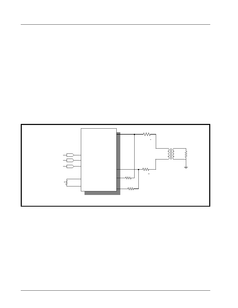
XRT75L02
áç
áç
áç
áç
TWO CHANNEL E3/DS3/STS-1 LINE INTERFACE UNIT WITH JITTER
REV. 1.0.1
26
For E3 rate, since the output pulse template is measured at the secondary of the transformer and since there is
no Cross-Connect system pulse template requirements, the Transmit Build Out Circuit is always disabled.
4.3.1
Guidelines for using Transmit Build Out Circuit:
If the distance between the transmitter and the DSX3 or STSX-1, Cross-Connect system, is less than 225 feet,
enable the Transmit Build Out Circuit by setting the TxLEV_n input pin "Low" (in Hardware Mode) or setting the
TxLEV_n control bit to "0" (in Host Mode).
If the distance between the transmitter and the DSX3 or STSX-1 is greater than 225 feet, disable the Transmit
Build Out Circuit.
4.3.2
Interfacing to the line:
The differential line driver increases the transmit waveform to appropriate level and drives into the 75
load as
shown in Figure 6.
4.4
Transmit Drive Monitor:
This feature is used for monitoring the transmit line for occurrence of fault conditions such as a short circuit on
the line or a defective line driver.
To activate this function, connect MTIP_n pins to the TTIP_n lines via a 270
resistor and MRing_n pins to
TRING_n lines via 270
resistor as shown in Figure 16.
When the MTIP_n and MRING_n are connected to the TTIP_n and TRING_n lines, the drive monitor circuit
monitors the line for transitions. The DMO_n (Drive Monitor Output) will be asserted "Low" as long as the
transitions on the line are detected via MTIP_n and MRING_n.
If no transitions on the line are detected for 128 ± 32 TxClk_n periods, the DMO_n output toggles "High" and
when the transitions are detected again, DMO_n toggles "Low".
N
OTES
:
1.
The Drive Monitor Circuit is only for diagnostic purpose and does not have to be used to operate the transmitter
.
2.
With TxMON pin "High", MTIP and MRING will be internally connected to TTIP and TRING for self-monitoring.
F
IGURE
16. T
RANSMIT
D
RIVER
M
ONITOR
SET
-
UP
.
3k
+ 1%
TTIP(n)
TRING(n)
XRT75L02 (0nly one channel shown)
1:1
R3
75
TxPOS(n)
TxNEG(n)
TxLineClk(n)
TPOS(n)
TNEG(n)
TxCLK(n)
RxB
RxA
31.6
+ 1%
31.6
+1%
R1
R2
MRING(n)
MTIP(n)
R5 270
R4 270

áç
áç
áç
áç
XRT75L02
REV. 1.0.1
TWO CHANNEL E3/DS3/STS-1 LINE INTERFACE UNIT WITH JITTER
27
4.5
Transmitter Section On/Off:
The transmitter section of each channel can either be turned on or off. To turn on the transmitter, set the input
pin TxON to "High" (in Hardware Mode) or in Host Mode set the TxON_n control bits and tie the TxON pins
"High"
When the transmitter is turned off, TTIP_n and TRING_n are tri-stated.
N
OTES
:
1.
This feature provides support for Redundancy.
2.
If configured in Host mode, to permit a system designed for redundancy to quickly shut-off the defective line card
and turn on the back-up line card, setting the TxON_n control bits transfers the control to TxON pins.
5.0
THE RECEIVER SECTION:
This section describes the detailed operation of the various blocks in the receiver. The receiver recovers the
TTL/CMOS level data from the incoming bipolar B3ZS or HDB3 encoded input pulses.
5.1
AGC/Equalizer:
The Adaptive Gain Control circuit amplifies the incoming analog signal and compensates for the various flat
losses and also for the loss at one-half symbol rate. The AGC has a dynamic range of 30 dB.
The Equalizer restores the integrity of the signal and compensates for the frequency dependent attenuation up
to 900 feet of coaxial cable (1300 feet for E3). The Equalizer also boosts the high frequency content of the
signal to reduce Inter-Symbol Interference (ISI) so that the slicer slices the signal at 50% of peak voltage to
generate Positive and Negative data.
The Equalizer can either be "IN" or "OUT" by setting the REQEN_n pin "High" or "Low" (in Hardware Mode) or
setting the REQEN_n control bit to "1" or "0" (in Host Mode).
R
ECOMMENDATIONS
FOR
E
QUALIZER
S
ETTINGS
:
The Equalizer has two gain settings to provide optimum equalization. In the case of normally shaped DS3/
STS-1 pulses (pulses that meet the template requirements) that has been driven through 0 to 900 feet of cable,
the Equalizer can be left "IN" by setting the REQEN_n pin to "High" (in Hardware Mode) or setting the
REQEN_n control bit to "1" (in Host Mode).
However, for square-shaped pulses such as E3 or for DS3/STS-1 high pulses (that does not meet the pulse
template requirements), it is recommended that the Equalizer be left "OUT" for cable length less than 300 feet
by setting the REQEN_n pin "Low" (in Hardware Mode) or by setting the REQEN_n control bit to "0" (in Host
Mode).This would help to prevent over-equalization of the signal and thus optimize the performance in terms of
better jitter transfer characteristics.
N
OTE
: The results of extensive testing indicates that even when the Equalizer was left "IN" (REQEN_n = "HIGH"),
regardless of the cable length, the integrity of the E3 signal was restored properly over 0 to 12 dB cable
loss at Industrial Temperature.
The Equalizer also contain an additional 20 dB gain stage to provide the line monitoring capability of the
resistively attenuated signals which may have 20dB flat loss. This capability can be turned on by setting the
RxMON_n bits in the control register or by setting the RxMON pin "High".
5.1.1
Interference Tolerance:
For E3 mode, ITU-T G.703 Recommendation specifies that the receiver be able to recover error-free clock and
data in the presence of a sinusoidal interfering tone signal. For DS3 and STS-1 modes, the same
recommendation is being used. Figure 17 shows the configuration to test the interference margin for DS3/
STS1. Figure 18 shows the set up for E3.
XRT75L02
áç
áç
áç
áç
TWO CHANNEL E3/DS3/STS-1 LINE INTERFACE UNIT WITH JITTER
REV. 1.0.1
28
5.2
Clock and Data Recovery:
The Clock and Data Recovery Circuit extracts the embedded clock, from the sliced digital data stream and
provides the retimed data to the B3ZS (HDB3) decoder.
The Clock Recovery PLL can be in one of the following two modes:
F
IGURE
17. I
NTERFERENCE
M
ARGIN
T
EST
S
ET
UP
FOR
DS3/STS-1
F
IGURE
18. I
NTERFERENCE
M
ARGIN
T
EST
S
ET
UP
FOR
E3.
T
ABLE
9: I
NTERFERENCE
M
ARGIN
T
EST
R
ESULTS
M
ODE
C
ABLE
L
ENGTH
(A
TTENUATION
)
I
NTERFERENCE
T
OLERANCE
E3
0 dB
-14 dB
12 dB
-18 dB
DS3
0 feet
-17 dB
225 feet
-16 dB
450 feet
-16dB
STS-1
0 feet
-16 dB
225 feet
-15 dB
450 feet
-15 dB
Test Equipment
Pattern Generator
2
23
-1 PRBS
Sine Wave
Generator
N
S
Cable Simulator
DUT
XRT75L02
Attenuator
DS3 = 22.368 MHz
STS-1 = 25.92 MHz
Test Equipment
Noise Generator
Pattern
Generator
N
S
Cable Simulator
DUT
XRT75L02
Attenuator 1
Attenuator 2
áç
áç
áç
áç
XRT75L02
REV. 1.0.1
TWO CHANNEL E3/DS3/STS-1 LINE INTERFACE UNIT WITH JITTER
29
T
RAINING
M
ODE
:
In the absence of input signals at RTIP_n and RRING_n pins, or when the frequency difference between the
recovered line clock signal and the reference clock applied on the E3/DS3/STS1CLK input pins exceed 0.5%, a
Loss of Lock condition is declared by toggling RLOL_n output pin "High" (in Hardware Mode) or setting the
RLOL_n bit to "1" in the control registers. Also, the clock output on the RxClk_n pins are the same as the
reference clock applied on E3/DS3/STS1CLK pins.
D
ATA
/C
LOCK
R
ECOVERY
M
ODE
:
In the presence of input line signals on the RTIP_n and RRING_n input pins and when the frequency difference
between the recovered clock signal and the reference clock signal is less than 0.5%, the clock that is output on
the RxClk_n out pins is the Recovered Clock signal.
5.3
B3ZS/HDB3 Decoder:
The decoder block takes the output from clock and data recovery block and decodes the B3ZS (for DS3 or
STS-1) or HDB3 (for E3) encoded line signal and detects any coding errors or excessive zeros in the data
stream.
When the input signal violates the B3ZS or HDB3 coding sequence for bipolar violation or contains three (for
B3ZS) or four (for HDB3) or more consecutive zeros, an active "High" pulse is generated on the RLCV_n output
pins to indicate line code violation.
N
OTE
: In Single- Rail (NRZ) mode, the decoder is bypassed.
5.4
LOS (Loss of Signal) Detector:
5.4.1
DS3/STS-1 LOS Condition:
A Digital Loss of SIgnal (DLOS) condition occurs when a string of 175 ± 75 consecutive zeros occur on the line.
When the DLOS condition occurs, the DLOS_n bit is set to "1" in the status control register. DLOS condition is
cleared when the detected average pulse density is greater than 33% for 175 ± 75 pulses.
Analog Loss of Signal (ALOS) condition occurs when the amplitude of the incoming line signal is below the
threshold as shown in the Table 10.The status of the ALOS condition is reflected in the ALOS_n status control
register.
RLOS is the logical OR of the DLOS and ALOS states. When the RLOS condition occurs the RLOS_n output
pin is toggled "High" and the RLOS_n bit is set to "1" in the status control register.
D
ISABLING
ALOS/DLOS D
ETECTION
:
For debugging purposes it is useful to disable the ALOS and/or DLOS detection. Setting both ALOSDIS_n and
DLOSDIS_n bits disables the LOS detection on a per channel basis.
5.4.2
E3 LOS Condition:
If the level of incoming line signal drops below the threshold as described in the ITU-T G.775 standard, the
LOS condition is detected. Loss of signal level is defined to be between 15 and 35 dB below the normal level. If
the signal drops below 35 dB for 175 ± 75 consecutive pulse periods, LOS condition is declared. This is
illustrated in Figure 19.
T
ABLE
10: T
HE
ALOS (A
NALOG
LOS) D
ECLARATION
AND
C
LEARANCE
T
HRESHOLDS
FOR
A
GIVEN
SETTING
OF
REQEN (DS3
AND
STS-1 A
PPLICATIONS
)
A
PPLICATION
REQEN S
ETTING
S
IGNAL
L
EVEL
TO
D
ECLARE
ALOS S
IGNAL
L
EVEL
TO
C
LEAR
ALOS
DS3
0
<17 mV
>70 mV
1
<20 mV
>90 mV
STS-1
0
<20 mV
>90 mV
1
<25 mV
>115 mV
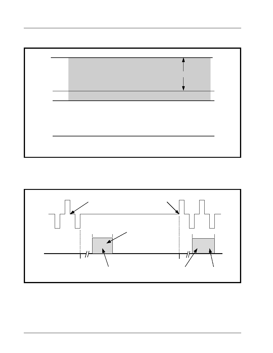
XRT75L02
áç
áç
áç
áç
TWO CHANNEL E3/DS3/STS-1 LINE INTERFACE UNIT WITH JITTER
REV. 1.0.1
30
As defined in ITU-T G.775, an LOS condition is also declared between 10 and 255 UI (or E3 bit periods) after
the actual time the LOS condition has occurred. The LOS condition is cleared within 10 to 255 UI after
restoration of the incoming line signal. Figure 20 shows the LOS declaration and clearance conditions.
5.4.3
Muting the Recovered Data with LOS condition:
When the LOS condition is declared, the clock recovery circuit locks into the reference clock applied to the E3/
DS3/STS1CLK pin and output this clock on the RxClk_n output. In Single Frequency Mode (SFM), the clock
recovery locks into the rate clock generated and output this clock on the RxClk_n pins. The data on the
RPOS_n and RNEG_n pins can be forced to zero by pulling the LOSMUT pin "High" (in Hardware Mode) or by
setting the LOSMUT_n bits in the individual channel control register to "1" (in Host Mode).
N
OTE
: When the LOS condition is cleared, the recovered data is output on RPOS_n and RNEG_n pins.
F
IGURE
19. L
OSS
O
F
S
IGNAL
D
EFINITION
FOR
E3
AS
PER
ITU-T G.775
F
IGURE
20. L
OSS
OF
S
IGNAL
D
EFINITION
FOR
E3
AS
PER
ITU-T G.775.
0 dB
-12 dB
-15dB
-35dB
Maximum Cable Loss for E3
LOS Signal Must be Declared
LOS Signal Must be Cleared
LOS Signal may be Cleared or Declared
Actual Occurrence
of LOS Condition
Line Signal
is Restored
Time Range for
LOS Declaration
Time Range for
LOS Clearance
G.775
Compliance
G.775
Compliance
0 UI
10 UI
0 UI
10 UI
255 UI
255 UI
RTIP/
RRing
RLOS Output Pin
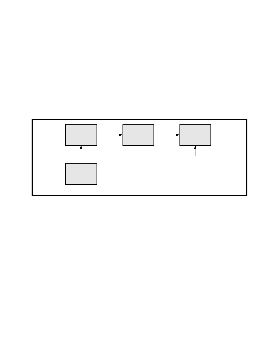
áç
áç
áç
áç
XRT75L02
REV. 1.0.1
TWO CHANNEL E3/DS3/STS-1 LINE INTERFACE UNIT WITH JITTER
31
6.0
JITTER:
There are three fundamental parameters that describe circuit performance relative to jitter:
·
Jitter Tolerance (Receiver)
·
Jitter Transfer (Receiver/Transmitter)
·
Jitter Generation
6.1
J
ITTER
T
OLERANCE
- R
ECEIVER
:
Jitter tolerance is a measure of how well a Clock and Data Recovery unit can successfully recover data in the
presence of various forms of jitter. It is characterized by the amount of jitter required to produce a specified bit
error rate. The tolerance depends on the frequency content of the jitter. Jitter Tolerance is measured as the
jitter amplitude over a jitter spectrum for which the clock and data recovery unit achieves a specified bit error
rate (BER). To measure the jitter tolerance as shown in Figure 21, jitter is introduced by the sinusoidal
modulation of the serial data bit sequence.
Input jitter tolerance requirements are specified in terms of compliance with jitter mask which is represented as
a combination of points.Each point corresponds to a minimum amplitude of sinusoidal jitter at a given jitter
frequency.
6.1.1
DS3/STS-1 Jitter Tolerance Requirements:
Bellcore GR-499 CORE, Issue 1, December 1995 specifies the minimum requirement of jitter tolerance for
Category I and Category II. The jitter tolerance requirement for Category II is the most stringent. Figure 22
shows the jitter tolerance curve as per GR-499 specification.
F
IGURE
21. J
ITTER
T
OLERANCE
M
EASUREMENTS
FREQ
Synthesizer
Pattern
Generator
DUT
XRT75L02
Error
Detector
Modulation
Freq.
Data
Clock

XRT75L02
áç
áç
áç
áç
TWO CHANNEL E3/DS3/STS-1 LINE INTERFACE UNIT WITH JITTER
REV. 1.0.1
32
6.1.2
E3 Jitter Tolerance Requirements:
ITU-T G.823 standard specifies that the clock and data recovery unit must be able to accommodate and
tolerate jitter up to certain specified limits. Figure 23 shows the tolerance curve.
As shown in the Figures 22 and 23 above, in the jitter tolerance measurement, the dark line indicates the
minimum level of jitter that the E3/DS3/STS-1 compliant component must tolerate.
The Table 11 below shows the jitter amplitude versus the modulation frequency for various standards.
F
IGURE
22. I
NPUT
J
ITTER
T
OLERANCE
F
OR
DS3/STS-1
F
IGURE
23. I
NPUT
J
ITTER
T
OLERANCE
FOR
E3
0 .0 1
0 .0 3
1 5
1 .5
0 .3
2
2 0
0 .1 5
J
I
TTER
AM
PL
I
T
U
D
E
(
U
I
pp
)
J IT T E R F R E Q U E N C Y (k H z )
1 0
5
0 .3
6 0
0 .1
G R -2 5 3 S T S -1
G R -4 9 9 C a t II
G R -4 9 9 C a t I
0 .1
1 .5
1
1 0
J
I
T
T
E
R AM
PL
I
T
U
D
E (
U
I
pp
)
J IT T E R F R E Q U E N C Y (k H z )
8 0 0
IT U -T G .8 2 3

áç
áç
áç
áç
XRT75L02
REV. 1.0.1
TWO CHANNEL E3/DS3/STS-1 LINE INTERFACE UNIT WITH JITTER
33
6.2
J
ITTER
T
RANSFER
- R
ECEIVER
/T
RANSMITTER
:
Jitter Transfer function is defined as the ratio of jitter on the output relative to the jitter applied on the input
versus frequency.
There are two distinct characteristics of jitter transfer: i) jitter gain (jitter peaking) defined as the highest ratio
above 0dB; and ii) jitter transfer bandwidth.The overall jitter transfer bandwidth is controlled by a low bandwidth
loop, typically using a voltage-controller crystal oscillator (VCXO).
The jitter transfer function is a ratio between the jitter output and jitter input for a component, or system often
expressed in dB. A negative dB jitter transfer indicates the element removed jitter. A positive dB jitter transfer
indicates the element added jitter. A zero dB jitter transfer indicates the element had no effect on jitter.
Table 12 shows the jitter transfer characteristics and/or jitter attenuation specifications for various data rates:
The above specifications can be met only with a jitter attenuator that supports E3/DS3/STS-1 rates.
6.3
J
ITTER
G
ENERATION
:
Jitter Generation is defined as the process whereby jitter appears at the output port of the digital equipment in
the absence of applied input jitter. Jitter Generation is measured by sending jitter free data to the clock and
data recovery circuit and measuring the amount of jitter on the output clock or the re-timed data. Since this is
essentially a noise measurement, it requires a definition of bandwidth to be meaningful. The bandwidth is set
according to the data rate. In general, the jitter is measured over a band of frequencies.
6.4
Jitter Attenuator:
An advanced crystal-less jitter attenuator per channel is included in the XRT75L02. The jitter attenuator
requires no external crystal nor high-frequency reference clock.
In Host mode, by clearing or setting the JATx/Rx_n bits in the channel control registers selects the jitter
attenuator either in the Receive or Transmit path on per channel basis. In Hardware mode, JATx/Rx pin selects
globally all three channels either in Receive or Transmit path.
The FIFO size can be either 16-bit or 32-bit. In HOST mode, the bits JA0_n and JA1_n can be set to
appropriate combination to select the different FIFO sizes or to disable the Jitter Attenuator on a per channel
basis. In Hardware mode, appropriate setting of the pins JA0 and JA1 selects the different FIFO sizes or
disables the Jitter Attenuator for all the channels. Data is clocked into the FIFO with the associated clock signal
(TxClk or RxClk) and clocked out of the FIFO with the dejittered clock. When the FIFO is within two bits of
T
ABLE
11: J
ITTER
A
MPLITUDE
VERSUS
M
ODULATION
F
REQUENCY
(J
ITTER
T
OLERANCE
)
B
IT
R
ATE
(
KB
/
S
)
S
TANDARD
I
NPUT
J
ITTER
A
MPLITUDE
(UI
P
-
P
)
M
ODULATION
F
REQUENCY
A1
A2
A3
F
1(H
Z
)
F
2(H
Z
)
F
3(
K
H
Z
)
F
4(
K
H
Z
)
F
5(
K
H
Z
)
34368
ITU-T G.823
1.5
0.15
-
100
1000
10
800
-
44736
GR-499
CORE Cat I
5
0.1
-
10
2.3k
60
300
-
44736
GR-499
CORE Cat II
10
0.3
-
10
669
22.3
300
-
51840
GR-253
CORE Cat II
15
1.5
0.15
10
30
300
2
20
T
ABLE
12: J
ITTER
T
RANSFER
S
PECIFICATION
/R
EFERENCES
E3
DS3
STS-1
ETSI TBR-24
GR-499 CORE section 7.3.2
Category I and Category II
GR-253 CORE section 5.6.2.1
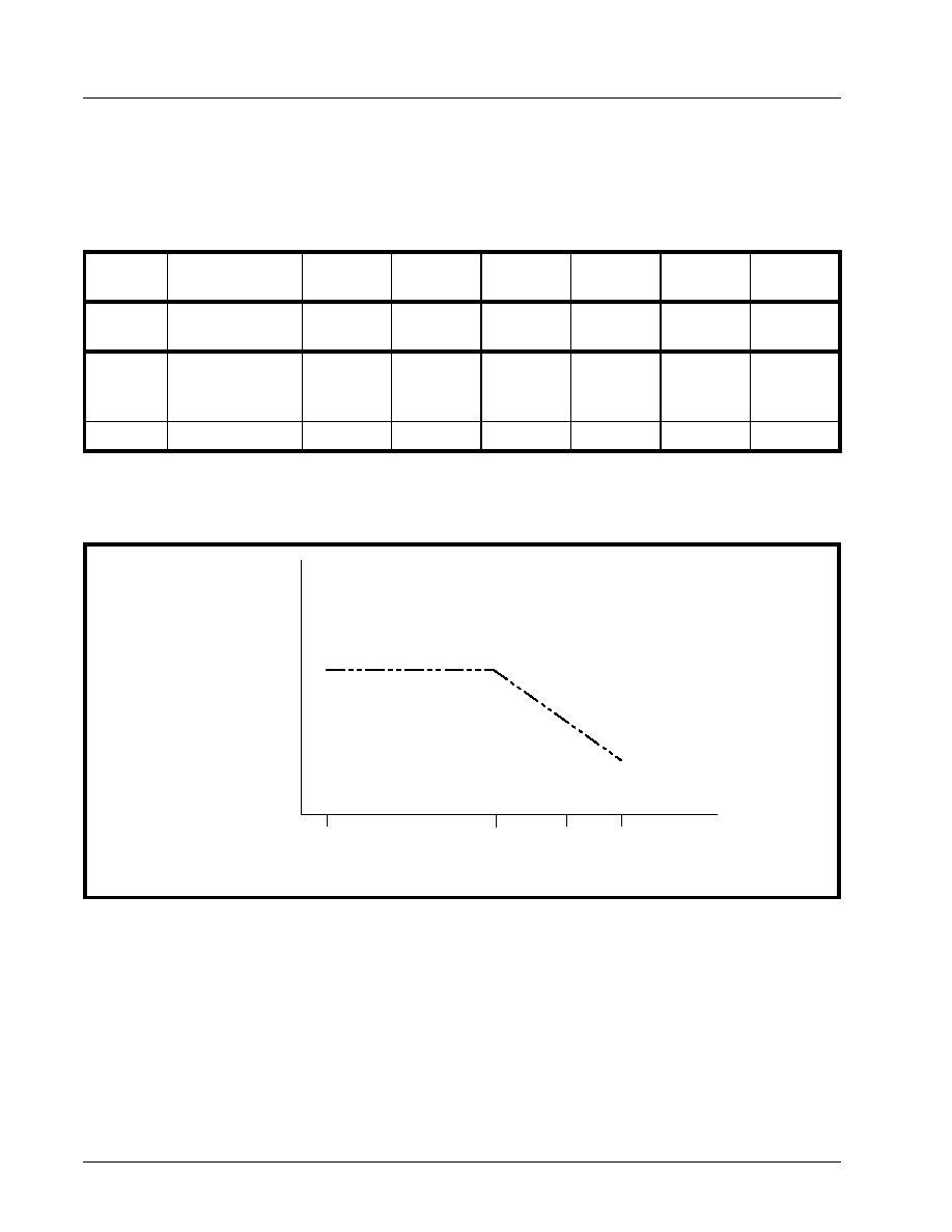
XRT75L02
áç
áç
áç
áç
TWO CHANNEL E3/DS3/STS-1 LINE INTERFACE UNIT WITH JITTER
REV. 1.0.1
34
overflowing or underflowing, the FIFO limit status bit, FL_n is set to "1" in the Alarm status register. Reading
this bit clears the FIFO and resets the bit into default state.
N
OTE
: It is recommended to select the 16-bit FIFO for delay-sensitive applications as well as for removing smaller amounts
of jitter. Table 13 specifies the jitter transfer mask requirements for various data rates:
The jitter attenuator in the XRT75L02 meets the latest jitter attenuation specifications and/or jitter transfer
characteristics as shown in the Figure 24.
T
ABLE
13: J
ITTER
T
RANSFER
P
ASS
M
ASKS
R
ATE
(
KBITS
)
M
ASK
F1
(H
Z
)
F2
(H
Z
)
F3
(H
Z
)
F4
(
K
H
Z
)
A1(dB)
A2(dB)
34368
G.823
ETSI-TBR-24
100
300
3
K
800
K
0.5
-19.5
44736
GR-499, Cat I
GR-499, Cat II
GR-253 CORE
10
10
10
10k
56.6k
40
-
-
-
15k
300k
15k
0.1
0.1
0.1
-
-
-
51840
GR-253 CORE
10
40k
-
400k
0.1
-
F
IGURE
24. J
ITTER
T
RANSFER
R
EQUIREMENTS
AND
J
ITTER
A
TTENUATOR
P
ERFORMANCE
F 1
A 1
F 2
J
I
T
T
E
R AM
PL
I
T
UDE
J I T T E R F R E Q U E N C Y ( k H z )
A 2
F 3
F 4

áç
áç
áç
áç
XRT75L02
REV. 1.0.1
TWO CHANNEL E3/DS3/STS-1 LINE INTERFACE UNIT WITH JITTER
35
7.0
SERIAL HOST INTERFACE:
A serial microprocessor interface is included in the XRT75L02. The interface is generic and is designed to
support the common microprocessors/microcontrollers. The XRT75L02 is configured in Host mode when the
HOST/HW pin is tied "High". The serial interface includes a serial clock (SClk), serial data input (SDI), serial
data output (SDO), chip select (CS) and interrupt output (INT). The serial interface timing is shown in Figure
11.
The active low interrupt output signal (INT pin) indicates alarm conditions like LOS, DMO and FL to the
processor.
When configured in Host mode, the following input pins,TxLEV_n, TAOS_n, RLB_n, LLB_n, E3_n, STS-1/
DS3_n, REQEN_n, JATx/Rx, JA0 and JA1 are disabled and must be connected to ground.
The Table 14 below illustrates the functions of the shared pins in either Host mode or in Hardware mode.
N
OTE
: While configured in Host mode, the TxON input pin will be active if the TxON_n bits in the control register are set to
"1", and can be used to turn on and off the transmit output drivers. This permits a system designed for redundancy
to quickly switch out a defective line card and switch-in the backup line card.
T
ABLE
14: F
UNCTIONS
OF
SHARED
PINS
P
IN
N
UMBER
I
N
H
OST
M
ODE
I
N
H
ARDWARE
M
ODE
29
CS
RxClkINV
30
SClk
TxClkINV
31
SDI
RxON
27
SDO
RxMON
28
INT
LOSMUT
T
ABLE
15: R
EGISTER
M
AP
AND
B
IT
N
AMES
A
DDRESS
(H
EX
)
P
ARAMETER
N
AME
D
ATA
B
ITS
7
6
5
4
3
2
1
0
0x00
APS/Redundancy
(read/write)
Reserved
RxON-1
RxON_0
Reserved
TxON-1
TxON_0
0x20
Interrupt Enable-
Global
(read/write)
Reserved
INTEN_1
INTEN_0
0x21
Interrupt Status
(read only)
Reserved
INTST_1
INTST_0
0x22-
0x3D
Reserved
Reserved
0x3E
Chip_id
(read only)
Device part number (7:0)
0x3F
Chip_version
(read only)
Chip revision number (7:0)
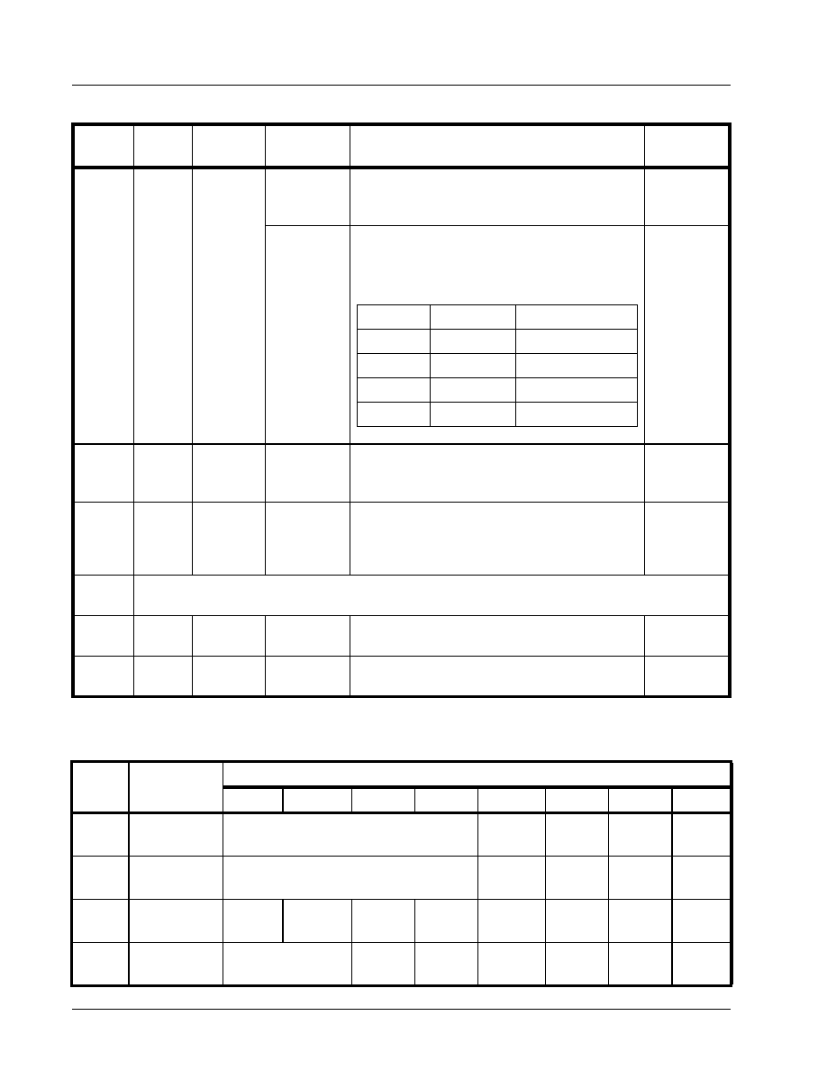
XRT75L02
áç
áç
áç
áç
TWO CHANNEL E3/DS3/STS-1 LINE INTERFACE UNIT WITH JITTER
REV. 1.0.1
36
T
ABLE
16: R
EGISTER
M
AP
D
ESCRIPTION
- G
LOBAL
A
DDRESS
(H
EX
)
T
YPE
R
EGISTER
N
AME
S
YMBOL
D
ESCRIPTION
D
EFAULT
V
ALUE
0x00
R/W
APS/Redu
ndancy
RxON_n
Bit 4 = RxON_0,Bit 5 = RxON_1
Receiver Turn On. Writing a "1" to the bit field turns
on the Receiver and a "0" turn off the Receiver.
0
TxON_n
Bit 0 = TxON_0, Bit 1 = TxON_1
Table below shows the status of the transmitter based
on the bit and pin setting.
0
0x20
R/W
Interrupt
Enable
INTEN_n
Bit 1 = INTEN_1, Bit 0 = INTEN_0.
Writing a "1" to these bits enable the interrupts for
the corresponding channels.
0
0x21
Read
Only
Interrupt
Status
INTST_n
Bit 1 = INTST_1, Bit 0 = INTST_0.
Respective bits are set to "1" if an interrupt service is
required. The respective source level interrupt status
registers are read to determine the cause of interrupt.
0
0x22 -
0x3D
Reserved
0x3E
Read
Only
Device
Number
Chip_id
This read only register contains device id.
0x3F
Read
Only
Version
Number
Chip_version
This read only register contains chip version number
T
ABLE
17: R
EGISTER
M
AP
AND
B
IT
N
AMES
- C
HANNEL
0 R
EGISTERS
A
DDRESS
(H
EX
)
P
ARAMETER
N
AME
D
ATA
B
ITS
7
6
5
4
3
2
1
0
0x01
Interrupt Enable
(read/write)
Reserved
FLIE_0
RLOLIE_0 RLOSIE_
0
DMOIE_0
0x02
Interrupt Status
(reset on read)
Reserved
FLIS_0
RLOLIS_0 RLOSIS_
0
DMOIS_0
0x03
Alarm Status
(read only)
Reserved PRBSLS_0
DLOS_0
ALOS_0
FL_0
RLOL_0
RLOS_0
DMO_0
0x04
Transmit Control
(read/write)
Reserved
TxMON_0 INSPRBS
_0
Reserved
TAOS_0
TxClkINV
_0
TxLEV_0
Bit
0
0
Transmitter Status
OFF
OFF
Pin
0
1
1
1
OFF
ON
0
1

áç
áç
áç
áç
XRT75L02
REV. 1.0.1
TWO CHANNEL E3/DS3/STS-1 LINE INTERFACE UNIT WITH JITTER
37
0x05
Receive Control
(read/write)
Reserved
DLOSDIS
_0
ALOSDIS
_0
RxClkINV_
0
LOSMUT_
0
RxMON_0 REQEN_
0
0x06
Block Control
(read/write)
Reserved
PRBSEN_
0
RLB_0
LLB_0
E3_0
STS1/
DS3_0
SR/DR_0
0x07
Jitter Attenuator
(read/write)
Reserved
DFLCK_0 PNTRST_
0
JA1_0
JATx/Rx_0
JA0_0
0x08
Reserved
Reserved
T
ABLE
18: R
EGISTER
M
AP
AND
B
IT
N
AMES
- C
HANNEL
1 R
EGISTERS
A
DDRESS
(H
EX
)
P
ARAMETER
N
AME
D
ATA
B
ITS
7
6
5
4
3
2
1
0
0x09
Interrupt Enable
(read/write)
Reserved
FLIE_1
RLOLIE_1 RLOSIE_
1
DMOIE_1
0x0A
Interrupt Status
(reset on read)
Reserved
FLIS_1
RLOLIS_1 RLOSIS_
1
DMOIS_1
0x0B
Alarm Status
(read only)
Reserved PRBSLS_
1
DLOS_1
ALOS_1
FL_1
RLOL_1
RLOS_1
DMO_1
0x0C
Transmit Con-
trol
(read/write)
Reserved
TxMON_1 INSPRBS
_1
Reserved
TAOS_1
TxClkINV
_1
TxLEV_1
0x0D
Receive Control
(read/write)
Reserved
DLOSDIS
_1
ALOSDIS
_1
RxClkINV
_1
LOSMUT_
1
RxMON_1 REQEN_1
0x0E
Block Control
(read/write)
Reserved
PRBSEN_
1
RLB_1
LLB_1
E3_1
STS1/
DS3_1
SR/DR_1
0x0F
Jitter Attenuator
(read/write)
Reserved
DFLCK_1 PNTRST_
1
JA1_1
JATx/Rx_1
JA0_1
0x10
Reserved
Reserved
T
ABLE
17: R
EGISTER
M
AP
AND
B
IT
N
AMES
- C
HANNEL
0 R
EGISTERS
A
DDRESS
(H
EX
)
P
ARAMETER
N
AME
D
ATA
B
ITS
7
6
5
4
3
2
1
0

XRT75L02
áç
áç
áç
áç
TWO CHANNEL E3/DS3/STS-1 LINE INTERFACE UNIT WITH JITTER
REV. 1.0.1
38
T
ABLE
19: R
EGISTER
M
AP
D
ESCRIPTION
- C
HANNEL
0
A
DDRESS
(H
EX
)
T
YPE
R
EGISTER
N
AME
BIT#
S
YMBOL
D
ESCRIPTION
D
EFAULT
V
ALUE
0x01 (ch 0)
0x09 (ch 1)
R/W
Interrupt
Enable
(source
level)
D0
DMOIE_n
Writing a "1" to this bit enables an interrupt when the
no transmission detected on channel output.
0
D1
RLOSIE_n Writing a "1" to this bit enables an interrupt when
Receive Los of Signal is detected.
0
D2
RLOLIE_n
Writing a "1" to this bit enables an interrupt when
Receive Loss of Lock condition is detected
0
D3
FLIE_n
Writing a "1" to this bit enables the interrupt when
the FIFO Limit of the Jitter Attenuator is within 2 bits
of overflow/underflow condition.
N
OTE
: This bit field is ignored when the Jitter
Attenuator is disabled.
0
D7-D4
Reserved
0x02 (ch 0)
0x0A (ch 1)
Reset
on
Read
Interrupt
Status
(source
level)
D0
DMOIS_n
This bit is set every time a DMO status change has
occurred since the last cleared interrupt.This bit is
cleared when the register bit is read.
0
D1
RLOSIS_n This bit is set every time a RLOS status change has
occurred since the last cleared interrupt. This bit is
cleared when the register bit is read.
0
D2
RLOLIS_n
This bit is set every time a RLOL status change has
occurred since the last cleared interrupt. This bit is
cleared when the register bit is read.
0
D3
FLIS_n
This bit is set every time a FIFO Limit status change
has occurred since the last cleared interrupt. This bit
is cleared when the register bit is read.
0
D7-D4
Reserved
0x03 (ch 0)
0x0B (ch 1)
Read
Only
Alarm Sta-
tus
D0
DMO_n
This bit is set every time the MTIP_0/MRing_0 input
pins have not detected any bipolar pulses for 128
consecutive bit periods.
0
D1
RLOS_n
This bit is set every time the receiver declares an
LOS condition.
0
D2
RLOL_n
This bit is set every time when the receiver declares
a Loss of Lock condition.
0
D3
FL_n
This bit is set every time the FIFO in the Jitter Atten-
uator is within 2 bit of underflow/overflow condition.
0
D4
ALOS_n
This bit is set every time the receiver declares Ana-
log LOS condition.
0
D5
DLOS_n
This bit is set every time the receiver declares Digital
LOS condition.
0
D6
PRBSLS_n This bit is set every time the PRBS detector is not in
sync.
0
D7
Reserved

áç
áç
áç
áç
XRT75L02
REV. 1.0.1
TWO CHANNEL E3/DS3/STS-1 LINE INTERFACE UNIT WITH JITTER
39
0x04 (ch 0)
0x0C (ch 1)
R/W
Transmit
Control
D0
TxLEV_n
Set this bit for cable length greater than 225
feet.
N
OTE
: See section 4.03 for detailed description.
0
D1
TxClkINV_
n
Set this bit to sample the data on TPOS/TNEG pins
on the rising edge of TxClk.
0
D2
TAOS_n
Set this bit to send a continuous stream of marks
(All Ones) out at the TTIP and TRING pins.
0
D3
Reserved
D4
INSPRBS_
n
Setting this bit causes the PRBS generator to insert
a single-bit error onto the transmit PRBS data
stream.
N
OTE
: PRBS Generator/Detector must be enabled
for this bit to have any effect.
0
D5
TxMON_n
Setting this bit causes the driver monitor its own
transmit driver. When the transmit failure is
detected, DMO output pin goes "High" and DMOIS
bit is set.
When this bit is "0", MTIP and MRing are connected
to other transmit channel for monitoring.
0
D7-D6
Reserved
0x05 (Ch 0)
0x0D (Ch 1)
R/W
Receive
Control
D0
REQEN_n
Set this bit to enable the Receive Equalizer.
N
OTE
: See section 5.01 for detailed description.
0
D1
RxMON_n
Set this bit to configure the Receiver in monitoring
mode. In this mode, the Receiver can monitor a sig-
nal at the RTIP/RRING pins that has be attenuated
up to 20dB flat loss.
0
D2
LOSMUT_
n
Setting this bit causes the RPOS/RNEG outputs to
"0" while the LOS condition is declared.
N
OTE
: If the bit has ben set, it will remain set even
after LOS condition is cleared.
0
D3
RxClkINV_
n
Set this bit to configure the Receiver to output
RPOS/RNEG data on the falling edge of RxClk_0.
0
D4
ALOSDIS_
n
Set this bit to disable the ALOS detector.
0
D5
DLOSDIS_
n
Set this bit to disable the DLOS detector.
0
D7-D6
Reserved
T
ABLE
19: R
EGISTER
M
AP
D
ESCRIPTION
- C
HANNEL
0
A
DDRESS
(H
EX
)
T
YPE
R
EGISTER
N
AME
BIT#
S
YMBOL
D
ESCRIPTION
D
EFAULT
V
ALUE

XRT75L02
áç
áç
áç
áç
TWO CHANNEL E3/DS3/STS-1 LINE INTERFACE UNIT WITH JITTER
REV. 1.0.1
40
0x06 (Ch 0)
0x0E (Ch 1)
R/W
Block Con-
trol
D0
SR/DR_n
Setting this bit configures the Receiver and Trans-
mitter in Single-Rail (NRZ) mode.
N
OTE
: See section 4.0 for detailed description.
0
D1
STS-1/
DS3_n
Setting this bit configures the channel into STS-1
mode.
N
OTE
: This bit field is ignored if the channel is
configured to operate in E3 mode.
0
D2
E3_n
Setting this bit configures the channel in E3 mode.
0
D3
LLB_n
Setting this bit configures the channel in Local Loop-
back mode.
0
D4
RLB_n
Setting this bit configures the channel in Remote
Loopback mode.
0
D5
PRBSEN_
n
Setting this bit enables the PRBS generator/detec-
tor. PRBS generator generate and detect either 2
15
-
1 (DS3 or STS-1) or 2
23
-1 (for E3).
The pattern generated and detected are unframed
pattern.
0
D7-D6
Reserved
T
ABLE
19: R
EGISTER
M
AP
D
ESCRIPTION
- C
HANNEL
0
A
DDRESS
(H
EX
)
T
YPE
R
EGISTER
N
AME
BIT#
S
YMBOL
D
ESCRIPTION
D
EFAULT
V
ALUE
RLB_n
0
0
Loopback Mode
Normal Operation
Analog Local
LLB_n
0
1
1
1
Remote
Digital
0
1
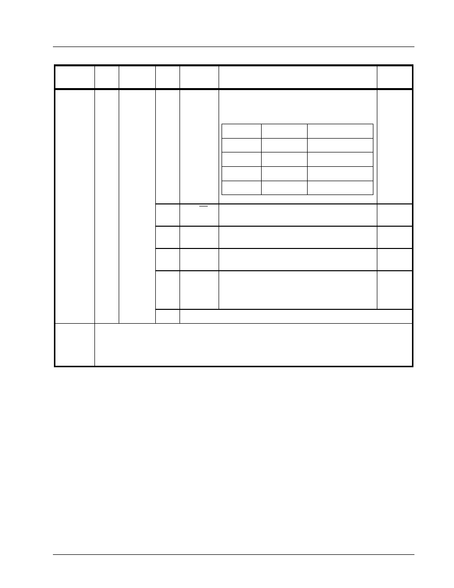
áç
áç
áç
áç
XRT75L02
REV. 1.0.1
TWO CHANNEL E3/DS3/STS-1 LINE INTERFACE UNIT WITH JITTER
41
0x07 (Ch 0)
0x0F (Ch 1)
R/W
Jitter
Attenuator
D0
JA0_n
This bit along with JA1_n bit configures the Jitter
Attenuator as shown in the table below.
0
D1
JATx/Rx_n Setting this bit selects the Jitter Attenuator in the
Transmit Path. A "0" selects in the Receive Path.
0
D2
JA1_n
This bit along with the JA0_n configures the Jitter
Attenuator as shown in the table.
0
D3
PNTRST_n Setting this bit resets the Read and Write pointers of
the jitter attenuator FIFO.
0
D4
DFLCK_n
Set this bit to "1" to disable fast locking of the PLL.
This helps to reduce the time for the PLL to lock to
incoming frequency when Jitter Attenuator switches
to narrow band.
0
D7-D5
Reserved
0x08
0x10
0x18 -
0x1f
Reserved
T
ABLE
19: R
EGISTER
M
AP
D
ESCRIPTION
- C
HANNEL
0
A
DDRESS
(H
EX
)
T
YPE
R
EGISTER
N
AME
BIT#
S
YMBOL
D
ESCRIPTION
D
EFAULT
V
ALUE
JA0_n
0
0
Mode
16 bit FIFO
32 bit FIFO
JA1_n
0
1
1
1
Disable Jitter
Attenuator
0
1
Disable Jitter
Attenuator
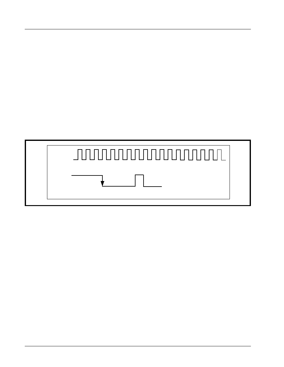
XRT75L02
áç
áç
áç
áç
TWO CHANNEL E3/DS3/STS-1 LINE INTERFACE UNIT WITH JITTER
REV. 1.0.1
42
8.0
DIAGNOSTIC FEATURES:
8.1
PRBS Generator and Detector:
The XRT75L02 contains an on-chip Pseudo Random Binary Sequence (PRBS) generator and detector for
diagnostic purpose. This feature is only available in Host mode. With the PRBSEN_n bit = "1", the transmitter
will send out PRBS of 2
23
-1 in E3 rate or 2
15
-1 in STS-1/DS3 rate. At the same time, the receiver PRBS
detector is also enabled. When the correct PRBS pattern is detected by the receiver, the RNEG/LCV pin will go
"Low" to indicate PRBS synchronization has been achieved. When the PRBS detector is not in sync the
PRBSLS bit will be set to "1" and RNEG/LCV pin will go "High".
With the PRBS mode enabled, the user can also insert a single bit error by toggling "INSPRBS" bit. This is
done by writing a "1" to INSPRBS bit. The receiver at RNEG/LCV pin will pulse "High" for one RxClk cycle for
every bit error detected. Any subsequent single bit error insertion must be done by first writing a "0" to
INSPRBS bit and followed by a "1".
Figure 25 shows the status of RNEG/LCV pin when the XRT75L02 is configured in PRBS mode.
N
OTE
: In PRBS mode, the device is forced to operate in Single-Rail Mode.
8.2
LOOPBACKS:
The XRT75L02 offers three loop back modes for diagnostic purposes. In Hardware mode, the loop back modes
are selected via the RLB_n and LLB_n pins. In Host mode, the RLB_n and LLB_n bits n the Channel control
registers select the loop back modes.
8.2.1
ANALOG LOOPBACK:
In this mode, the transmitter outputs (TTIP_n and TRING_n) are connected internally to the receiver inputs
(RTIP_n and RRING_n) as shown in Figure 26. Data and clock are output at RCLK_n, RPOS_n and RNEG_n
pins for the corresponding transceiver. Analog loop back exercises most of the functional blocks of the device
including the jitter attenuator which can be selected in either the transmit or receive path.
XRT75L02 can be configured in Analog Loopback either in Hardware mode via the LLB_n and RLB_n pins or
in Host mode via LLB_n and RLB_n bits in the channel control registers.
N
OTES
:
1.
In the Analog loopback mode, data is also output via TTIP_n and TRING_n pins.
2.
Signals on the RTIP_n and RRING_n pins are ignored during analog loop back.
F
IGURE
25. PRBS MODE
RClk
RNEG/LCV
SYNC LOSS
PRBS SYNC
Single Bit Error
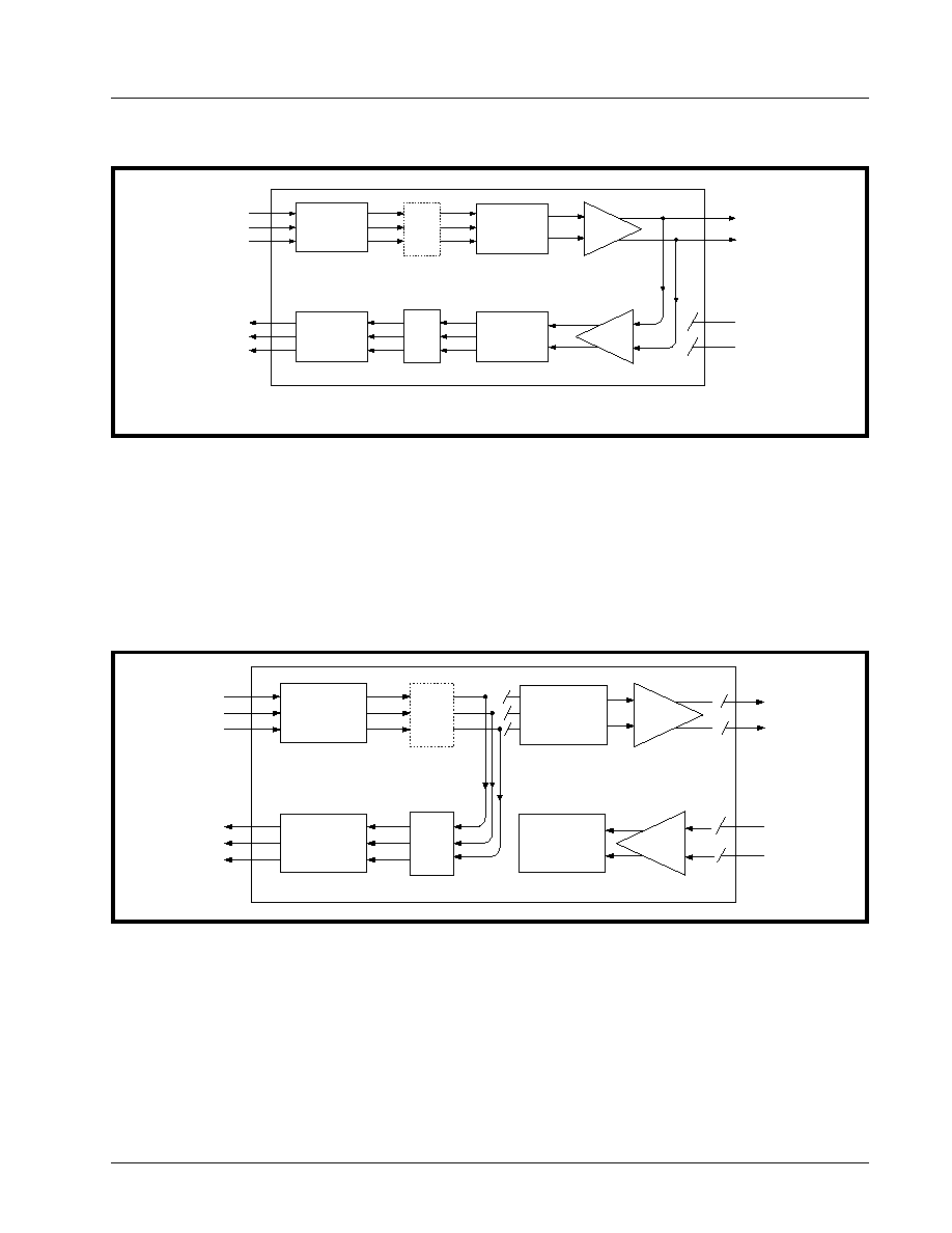
áç
áç
áç
áç
XRT75L02
REV. 1.0.1
TWO CHANNEL E3/DS3/STS-1 LINE INTERFACE UNIT WITH JITTER
43
8.2.2
DIGITAL LOOPBACK:
The Digital Loopback function is available either in Hardware mode or Host mode. When the Digital Loopback
is selected, the transmit clock (TxClk_n) and transmit data inputs (TPOS_n & TNEG_n) are looped back and
output onto the RxClk_n, RPOS_n and RNEG_n pins as shown in Figure 27. The data presented on TxClk,
TPOS and TNEG are not output on the TTIP and TRING pins.This provides the capability to configure the
protection card (in redundancy applications) in Digital Loopback mode without affecting the traffic on the
primary card.
N
OTE
: Signals on the RTIP_n and RRING_n pins are ignored during digital loop back.
8.2.3
IREMOTE LOOPBACK:
With Remote loop back activated as shown in Figure 28, the receive data on RTIP and RRING is looped back
after the jitter attenuator (if selected in receive or transmit path) to the transmit path using RxClk as transmit
timing. The receive data is also output via the RPOS and RNEG pins.
During the remote loop back mode, if the jitter attenuator is selected in the transmit path, the receive data after
the Clock and Data Recovery Block is looped back to the transmit path and passed through the jitter attenuator
using RxClk as the transmit timing.
N
OTE
: Input signals on TxClk, TPOS and TNEG are ignored during Remote loop back.
F
IGURE
26. A
NALOG
L
OOPBACK
F
IGURE
27. D
IGITAL
L
OOPBACK
TRING
TTIP
RRING
RTIP
RPOS
RNEG
RCLK
TNDATA
TCLK
TPDATA
HDB3/B3ZS
ENCODER
HDB3/B3ZS
DECODER
JITTE
R
2
ATTE
NUATOR
JITTE
R
2
ATTE
NUATOR
TIMING
CONTROL
DATA &
CLOCK
RECOVERY
1
if enabled
2
if enabled and selected in either Receive or Transmit path
Tx
Rx
1
1
TRING
TTIP
RRING
RTIP
RPOS
RNEG
RCLK
TNDATA
TCLK
TPDATA
HDB3/B3ZS
ENCODER
HDB3/B3ZS
DECODER
J
I
TTE
R
2
ATT
E
NUATO
R
J
I
TTE
R
2
ATT
E
NUATO
R
TIMING
CONTROL
DATA &
CLOCK
RECOVERY
1
if enabled
2
if enabled and selected in either Receive or Transmit path
Tx
Rx
1
1
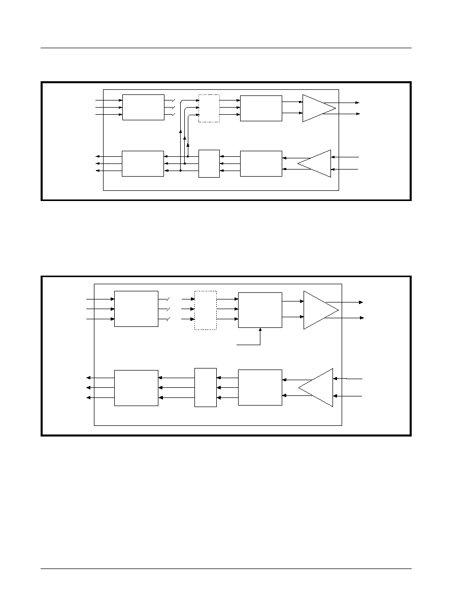
XRT75L02
áç
áç
áç
áç
TWO CHANNEL E3/DS3/STS-1 LINE INTERFACE UNIT WITH JITTER
REV. 1.0.1
44
8.3
TRANSMIT ALL ONES (TAOS):
Transmit All Ones (TAOS) can be set either in Hardware mode by pulling the TAOS_n pins "High" or in Host
mode by setting the TAOS_n control bits to "1" in the Channel control registers. When the TAOS is set, the
Transmit Section generates and transmits a continuous AMI all "1's" pattern on TTIP_n and TRING_n pins. The
frequency of this "1's" pattern is determined by TxClk_n.TAOS data path is shown in Figure 29.
F
IGURE
28. R
EMOTE
L
OOPBACK
F
IGURE
29. T
RANSMIT
A
LL
O
NES
(TAOS)
TRING
TTIP
RRING
RTIP
RPOS
RNEG
RCLK
TNDATA
TCLK
TPDATA
HDB3/B3ZS
ENCODER
HDB3/B3ZS
DECODER
JITTER
2
ATTENUATOR
JITTER
2
ATTENUATOR
TIMING
CONTROL
DATA &
CLOCK
RECOVERY
1
if enabled
2
if enabled and selected in either Receive or
Transmit path
Tx
Rx
1
1
TRING
TTIP
RRING
RTIP
RPOS
RNEG
RCLK
TNDATA
TCLK
TPDATA
HDB3/B3ZS
ENCODER
HDB3/B3ZS
DECODER
JITTER
2
ATTENUATOR
JITTER
2
ATTENUATOR
TIMING
CONTROL
DATA &
CLOCK
RECOVERY
1
if enabled
2
if enabled and selected in either Receive or
Transmit path
Tx
Rx
TAOS
Transmit All 1'
1
1

áç
áç
áç
áç
XRT75L02
REV. 1.0.1
TWO CHANNEL E3/DS3/STS-1 LINE INTERFACE UNIT WITH JITTER
45
APPENDIX B
TRANSFORMER VENDOR INFORMATION
Pulse
Corporate Office
12220 World Trade Drive
San Diego, CA 92128
Tel: (858)-674-8100
FAX: (858)-674-8262
Europe
1 & 2 Huxley Road
The Surrey Research Park
Guildford, Surrey GU2 5RE
United Kingdom
Tel: 44-1483-401700
FAX: 44-1483-401701
T
ABLE
20: TRANSFORMER RECOMMENDATIONS
P
ARAMETER
V
ALUE
Turns Ratio
1:1
Primary Inductance
40
µ
H
Isolation Voltage
1500 Vrms
Leakage Inductance
0.6
µ
H
T
ABLE
21: T
RANSFORMER
D
ETAILS
P
ART
N
UMBER
V
ENDOR
I
NSULATION
P
ACKAGE
T
YPE
PE-68629
PULSE
3000 V
Large Thru-hole
PE-65966
PULSE
1500 V
Samll Thru-hole
PE-65967
PULSE
1500 V
SMT
T 3001
PULSE
1500 V
SMT
TG01-0406NS
HALO
1500 V
SMT
TTI 7601-SM
TransPower
1500 V
SMT

XRT75L02
áç
áç
áç
áç
TWO CHANNEL E3/DS3/STS-1 LINE INTERFACE UNIT WITH JITTER
REV. 1.0.1
46
Asia
150 Kampong Ampat
#07-01/02
KA Centre
Singapore 368324
Tel: 65-287-8998
Website: http://www.pulseeng.com
Halo Electronics
Corporate Office
P.O. Box 5826
Redwood City, CA 94063
Tel: (650)568-5800
FAX: (650)568-6165
Email: info@haloelectronics.com
Website: http://www.haloelectronics.com
Transpower Technologies, Inc.
Corporate Office
Park Center West Building
9805 Double R Blvd, Suite # 100
Reno, NV 89511
(800)500-5930 or (775)852-0140
Email: info@trans-power.com
Website: http://www.trans-power.com
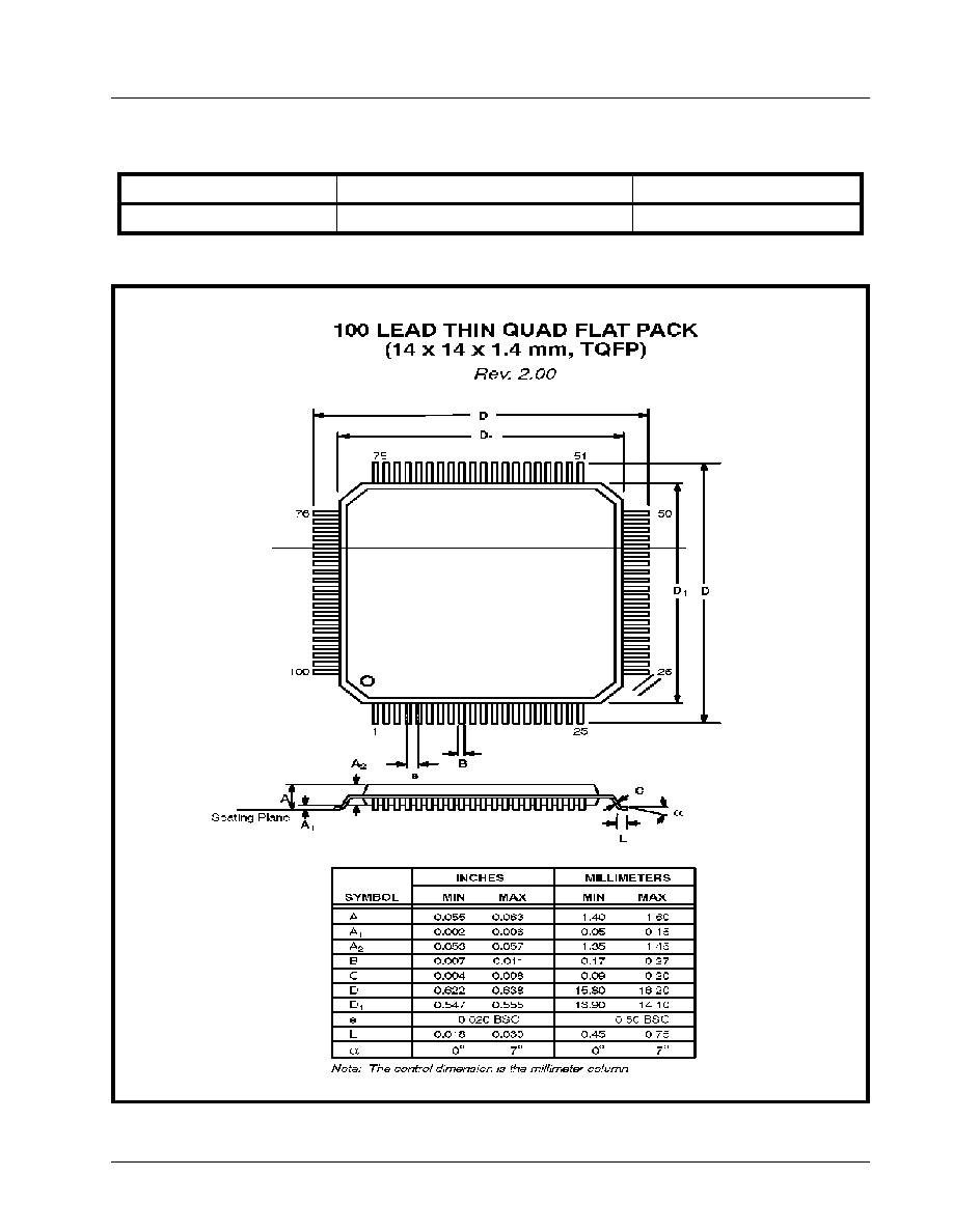
áç
áç
áç
áç
XRT75L02
REV. 1.0.1
TWO CHANNEL E3/DS3/STS-1 LINE INTERFACE UNIT WITH JITTER
47
ORDERING INFORMATION
PACKAGE DIMENSIONS
P
ART
N
UMBER
P
ACKAGE
T
YPE
O
PERATING
T
EMPERATURE
R
ANGE
XRT75L02IV
14x14 mm, 100 Lead Plastic QFP
-40°C to +85°C

XRT75L02
áç
áç
áç
áç
TWO CHANNEL E3/DS3/STS-1 LINE INTERFACE UNIT WITH JITTER
REV. 1.0.1
48
NOTICE
EXAR Corporation reserves the right to make changes to the products contained in this publication in order to
improve design, performance or reliability. EXAR Corporation assumes no responsibility for the use of any
circuits described herein, conveys no license under any patent or other right, and makes no representation that
the circuits are free of patent infringement. Charts and schedules contained here in are only for illustration
purposes and may vary depending upon a user's specific application. While the information in this publication
has been carefully checked; no responsibility, however, is assumed for inaccuracies.
EXAR Corporation does not recommend the use of any of its products in life support applications where the
failure or malfunction of the product can reasonably be expected to cause failure of the life support system or to
significantly affect its safety or effectiveness. Products are not authorized for use in such applications unless
EXAR Corporation receives, in writing, assurances to its satisfaction that: (a) the risk of injury or damage has
been minimized; (b) the user assumes all such risks; (c) potential liability of EXAR Corporation is adequately
protected under the circumstances.
Copyright 2003 EXAR Corporation
Datasheet November 2003.
Reproduction, in part or whole, without the prior written consent of EXAR Corporation is prohibited.
REVISION HISTORY
Package dimension was changed from 14 x 20 to 14 x 14.
1.0.1 Changed I
CC
and P
DD
in the electrical characteristics. Removed preliminary.