Untitled Document
Exar
Corporation 48720 Kato Road, Fremont CA, 94538
·
(510) 668-7000
·
FAX (510) 668-7017
·
www.exar.com
XRT73L04A
4 CHANNEL DS3/E3/STS-1 LINE INTERFACE UNIT
OCTOBER 2003
REV. 2.0.3
GENERAL DESCRIPTION
The XRT73L04A, 4-Channel, DS3/E3/STS-1 Line In-
terface Unit is an improved version of the XRT73L04
and consists of four independent line transmitters and
receivers integrated on a single chip designed for
DS3, E3 or SONET STS-1 applications.
Each channel of the XRT73L04A can be configured
to support the E3 (34.368 Mbps), DS3 (44.736 Mbps)
or the SONET STS-1 (51.84 Mbps) rates. Each
channel can be configured to operate in a mode/data
rate that is independent of the other channels.
In the transmit direction, each channel encodes input
data to either B3ZS (DS3/STS-1) or HDB3 (E3) for-
mat and converts the data into the appropriate pulse
shapes for transmission over coaxial cable via a 1:1
transformer.
In the receive direction, the XRT73L04A performs
equalization on incoming signals, performs Clock Re-
covery, decodes data from either B3ZS or HDB3 for-
mat, converts the receive data into TTL/CMOS for-
mat, checks for LOS or LOL conditions and detects
and declares the occurrence of Line Code Violations.
FEATURES
· Incorporates an improved Timing Recovery circuit
and is pin and functional compatible to XRT73L04
· Meets E3/DS3/STS-1 Jitter Tolerance Require-
ments
· Contains a 4-Wire Microprocessor Serial Interface
· Full Loop-Back Capability
· Transmit and Receive Power Down Modes
· Full Redundancy Support
· Uses Minimum External components
· Single +3.3V Power Supply
· 5V tolerant I/O
· -40°C to +85°C Operating Temperature Range
· Available in a Thermally Enhanced 144 pin TQFP
package
APPLICATIONS
· Digital Cross Connect Systems
· CSU/DSU Equipment
· Routers
· Fiber Optic Terminals
· Multiplexers
· ATM Switches
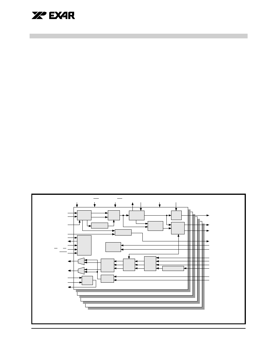
F
IGURE
1. XRT73L04A B
LOCK
D
IAGRAM
RLOS_(n)
LLB_(n)
RLB_(n)
TAOS_(n)
TPData_(n)
TNData_(n)
TxClk_(n)
TxLEV_(n)
TxOFF
Channel 2
AGC/
Equalizer
Serial
Processor
Interface
Peak
Detector
LOS Detector
Slicer
Clock
Recovery
Data
Recovery
Invert
Loop MUX
HDB3/
B3ZS
Decoder
LOSTHR
SDI
SDO
SClk
CS/(SR/DR)
REGR
RTIP_(n)
RRing_(n)
REQEN_(n)
Channel 0
Channel 1
Notes: 1. (n) = 0, 1, 2 , or 3 for respective Channels
2. Serial Processor Interface input pins are shared by the four Channels in HOST Mode and redefined in
Hardware Mode.
Device
Monitor
MTIP_(n)
MRing_(n)
DMO_(n)
Transmit
Logic
Duty Cycle Adjust
TTIP_(n)
TRing_(n)
Pulse
Shaping
HDB3/
B3ZS
Encoder
E3_(n)
STS-1/DS3_(n)
Host/(HW)
RLOL_(n) EXClk_(n)
RxOFF
RxClkINV
RxClk_(n)
RPOS_(n)
RNEG_(n)/
(LCV_(n))
Channel 3
Tx
Control
XRT73L04A
4 CHANNEL DS3/E3/STS-1 LINE INTERFACE UNIT
REV. 2.0.3
2
TYPICAL APPLICATIONS
TRANSMIT INTERFACE CHARACTERISTICS:
· Accepts either Single-Rail or Dual-Rail data from
Terminal Equipment and generates a bipolar signal
from the line
· Integrated Pulse Shaping Circuit
· Built-in B3ZS/HDB3 Encoder (which can be dis-
abled)
· Contains Transmit Clock Duty Cycle Correction Cir-
cuit on-chip
· Generates pulses that comply with the ITU-T G.703
pulse template (E3 applications)
· Generates pulses that comply with the DSX-3 pulse
template as specified in Bellcore GR-499
-CORE
and ANSI T1.102_1993
· Generates pulses that comply with the STSX-1
pulse template as specified in Bellcore GR-253-
CORE
· Transmitter can be turned off in order to support
redundancy designs
RECEIVE INTERFACE CHARACTERISTICS:
· Integrated Adaptive Receive Equalization (optional)
and Timing Recovery
· Declares and Clears the LOS defect per ITU-T
G.775 requirements (E3 and DS3 applications)
· Meets Jitter Tolerance Requirements as specified in
ITU-T G.823_1993 (E3 Applications)
· Meets Jitter Tolerance Requirements as specified in
Bellcore GR-499-CORE (DS3 Applications)
· Declares Loss of Signal (LOS) and Loss of Lock
(LOL) Alarms
· Built-in B3ZS/HDB3 Decoder (which can be dis-
abled)
· Recovered Data can be muted while the LOS Con-
dition is declared
· Outputs either Single-Rail or Dual-Rail data to the
Terminal Equipment
· Receiver can be powered down in order to con-
serve power in redundancy designs
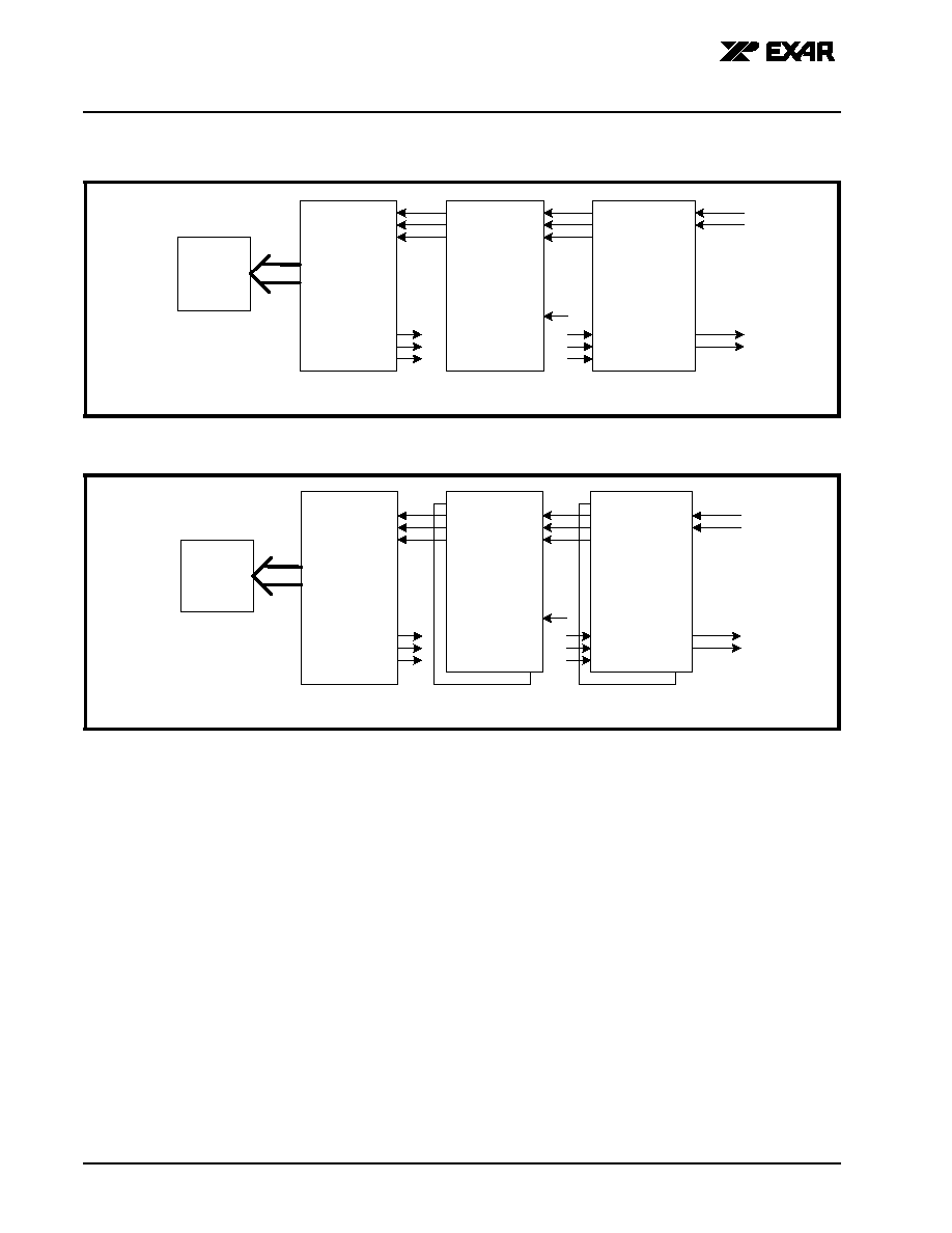
F
IGURE
2. M
ULTI
C
HANNEL
ATM A
PPLICATION
ATM
Sw itch/
SAR
XRT72L74
RPO S
RNEG
RxLineC lk
XRT71D04
XRT73L04A
RRPOS
RRNEG
RRClk
RPOS
RN EG
R xClk
RPOS
RNEG
RxClk
R TIP
R Ring
TTIP
TRing
TPO S
TNEG
TxLineC lk
MClk
TPO S
TNEG
TxClk
4 Channel DS 3 A TM UNI
4 Channel E3/DS3 J/A
4 Channel E 3/DS 3 LIU
F
IGURE
3. M
ULTI
S
ERVICE
- F
RAME
R
ELAY
A
PPLICATION
Fram e
Relay
XRT72L58
RPO S
RNE G
RxLineClk
XRT71D04
XRT73L04A
RRPOS
RRNE G
RRClk
RPOS
RNEG
RxClk
RP OS
RNEG
RxClk
RTIP
RRing
TTIP
TRing
TPO S
TNE G
TxLineClk
M Clk
TP OS
TNEG
TxClk
8 Channel E3/DS3 Fram er
2 x 4 Channel E3/DS3 J/A
2 x 4 Channel E3/DS3 LIU
XRT73L04A
4 CHANNEL DS3/E3/STS-1 LINE INTERFACE UNIT
REV. 2.0.3
3
ORDERING INFORMATION
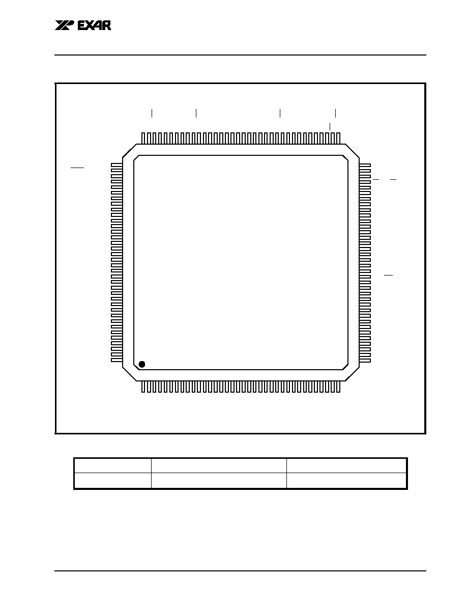
F
IGURE
4. P
IN
OUT
OF
THE
XRT73L04A
IN
THE
144 P
IN
TQFP
PACKAGE
1
2
3
4
5
6
7
8
9
10
11
12
13
14
15
16
17
18
19
20
21
22
23
24
25
26
27
28
29
30
31
32
33
34
35
36
72
71
70
69
68
67
66
65
64
63
62
61
60
59
58
57
56
55
54
53
52
51
50
49
48
47
46
45
44
43
42
41
40
39
38
37
108
107
106
105
104
103
102
101
100
99
98
97
96
95
94
93
92
91
90
89
88
87
86
85
84
83
82
81
80
79
78
77
76
75
74
73
109
110
111
112
113
114
115
116
117
118
119
120
121
122
123
124
125
126
127
128
129
130
131
132
133
134
135
136
137
138
139
140
141
142
143
144
XRT73L04A
MR
ing_2
MTIP
_2
TTIP_2
T
x
A
V
DD_
2
TR
ing_2
T
x
A
G
ND_
2
T
x
Clk_3
TP
D
a
ta_3
T
NDa
t
a
_
3
T
x
A
V
DD_
3
DM
O_
3
TTIP_3
T
x
A
V
DD_
3
TR
ing_3
T
x
A
G
ND_
3
MTIP
_3
MR
ing_3
T
x
A
G
ND_
3
T
x
A
G
ND_
1
MR
ing_1
MTIP
_1
T
x
A
G
ND_
1
TR
ing_1
T
x
A
V
DD_
1
TTIP_1
DM
O_
1
T
x
A
V
DD_
1
T
NDa
t
a
_
1
TP
D
a
ta_1
T
x
Clk_1
T
x
A
G
ND_
0
TR
ing_0
T
x
A
V
DD_
0
TTIP_0
MTIP
_0
MR
ing_0
E
3_2
E
3_3
STS1
/
D
S3
_
2
LLB
_2
RL
B
_
2
RxA
V
DD_
2
R
R
i
ng_2
RT
I
P
_
2
RxA
G
ND_
2
RE
QE
N_
2
STS1
/
D
S3
_
3
LLB
_3
RL
B
_
3
RxA
V
DD_
3
R
R
i
ng_3
RT
I
P
_
3
RxA
G
ND_
3
RE
QE
N_
3
RE
QE
N_
1
RxA
G
ND_
1
RT
I
P
_
1
R
R
i
ng_1
RxA
V
DD_
1
RL
B
_
1
LLB
_1
STS1
/
D
S3
_
1
RE
QE
N_
0
RxA
G
ND_
0
RT
I
P
_
0
R
R
i
ng_0
RxA
V
DD_
0
RL
B
_
0
LLB
_0
LOS
T
H
R
IC
T
STS1
/
D
S3
_
0
AGND_2
REGR/(RxClkINV)
LOSMUTEN
AGND_3
RLOL_3
RLOS_3
EXClk_2
RLOL_2
RLOS_2
RxDGND_2
RPOS_2
RNEG_2/LCV_2
RxClk_2
RxDVDD_2
EXClk_3
RxDGND_3
RPOS_3
RNEG3/LCV_3
RxClk_3
RxDVDD_3
EXDGNDA
EXDVDDA
TxOFF
TxAGND_2
DMO_2
TxAVDD_2
TAOS_2
TAOS_3
TxLEV_2
TxLEV_3
TxClk_2
TPData_2
TNData_2
NC
NC
NC
SDO/E3_0
SDI/E3_1
SClk/(RxOFF)
CS/(SR/DR)
RLOL_1
RLOS_1
EXClk_0
RLOL_0
RLOS_0
AGND_1
RxDGND_0
RPOS_0
RNEG_0/LCV_0
RxClk_0
RxDVDD_0
EXClk_1
RxDGND_1
RPOS_1
RNEG_1/LCV_1
RxClk_1
Host/(HW)
RxDVDD_1
AGND_0
TxAGND_0
DMO_0
TxAVDD_0
TAOS_0
TAOS_1
TxLEV_0
TxLEV_1
TxClk_0
TPData_0
TNData_0
NC
NC
NC
P
ART
#
P
ACKAGE
O
PERATING
TEMPERATURE
R
ANGE
XRT73L04AIV
144 Pin TQFP 20 X 20 X 1.4 mm
-40
o
C to +85
o
C

XRT73L04A
4 CHANNEL DS3/E3/STS-1 LINE INTERFACE UNIT
REV. 2.0.3
I
TABLE OF CONTENTS
G
ENERAL
DESCRIPTION
......................................................................................................... 1
F
EATURES
.................................................................................................................................................... 1
APPLICATIONS ......................................................................................................................................... 1
Figure 1.XRT73L04A Block Diagram ................................................................................................................ 1
T
YPICAL
A
PPLICATIONS
................................................................................................................................. 2
Figure 2.MultiChannel ATM Application ............................................................................................................ 2
Figure 3.MultiService - Frame Relay Application .............................................................................................. 2
T
RANSMIT
I
NTERFACE
C
HARACTERISTICS
: ..................................................................................................... 2
R
ECEIVE
I
NTERFACE
C
HARACTERISTICS
: ....................................................................................................... 2
Figure 4.Pin out of the XRT73L04A in the 144 Pin TQFP package .................................................................. 3
O
RDERING
INFORMATION
....................................................................................................... 3
TABLE OF CONTENTS ....................................................................................................... I
P
IN
D
ESCRIPTIONS
(
BY
FUNCTION
) ......................................................................................... 4
T
RANSMIT
I
NTERFACE
................................................................................................................................... 4
R
ECEIVE
I
NTERFACE
..................................................................................................................................... 6
C
LOCK
I
NTERFACE
........................................................................................................................................ 7
O
PERATING
M
ODE
S
ELECT
........................................................................................................................... 8
C
ONTROL
AND
A
LARM
I
NTERFACE
................................................................................................................. 9
M
ICROPROCESSOR
I
NTERFACE
.................................................................................................................... 11
P
OWER
AND
G
ROUND
P
INS
......................................................................................................................... 13
N
O
C
ONNECTION
P
INS
................................................................................................................................ 14
E
LECTRICAL
CHARACTERISTICS
........................................................................................... 15
A
BSOLUTE
M
AXIMUM
R
ATINGS
.................................................................................................................... 15
DC Electrical Characteristics .......................................................................................................... 15
AC Electrical Characteristics (See Figure 5) ........................................................................................................ 16
Terminal Side Timing Parameters (See Figure 6 and Figure 7) -- {(n) = 0, 1, 2 or 3 } ......................................... 16
Figure 5.Transmit Pulse Amplitude Test Circuit for E3, DS3 and STS-1 Rates (typical channel) .................. 17
Figure 6.Timing Diagram of the Transmit Terminal Input Interface ................................................................. 17
Figure 7.Timing Diagram of the Receive Terminal Output Interface ............................................................... 17
Line Side Parameters E3 Application ................................................................................................................... 18
Transmit Characteristics (see Figure 5) ............................................................................................................... 18
Line Side Parameters Sonet STS-1 Application ................................................................................................... 19
Transmit Characteristics (See Figure 5) ............................................................................................................... 19
Line Side Parameters DS3 Application ................................................................................................................ 20
Transmit Characteristics (see Figure 5) ............................................................................................................... 20
Figure 8.ITU-T G.703 Transmit Output Pulse Template for E3 Applications .................................................. 21
Figure 9.Bellcore GR-499-CORE Transmit Output Pulse Template for DS3 Applications ............................. 21
Figure 10.Bellcore GR-253-CORE Transmit Output Pulse Template for SONET STS-1 Applications ........... 22
Figure 11.Microprocessor Serial Interface Data Structure .............................................................................. 22
Microprocessor Serial Interface Timing (See Figure 12) ...................................................................................... 23
Figure 12.Timing Diagram for the Microprocessor Serial Interface ................................................................. 23
SYSTEM DESCRIPTION .................................................................................................. 24
T
HE
T
RANSMIT
S
ECTION
- C
HANNELS
0, 1, 2,
AND
3 .................................................................................... 24
T
HE
R
ECEIVE
S
ECTION
- C
HANNELS
0, 1, 2
AND
3 ....................................................................................... 24
T
HE
M
ICROPROCESSOR
S
ERIAL
I
NTERFACE
................................................................................................. 24
Table 1:Role of Microprocessor Serial Interface pins when the XRT73L04A is operating in the Hardware Mode
24
Figure 13.Functional Block Diagram of the XRT73L04A ................................................................................ 25

XRT73L04A
4 CHANNEL DS3/E3/STS-1 LINE INTERFACE UNIT
REV. 2.0.3
II
1.0 SELECTING THE DATA RATE ............................................................................................................... 25
1.1 C
ONFIGURING
C
HANNEL
(
N
) ............................................................................................................ 25
Table 2:Hexadecimal Addresses and Bit Formats of XRT73L04A Command Registers ............................... 26
Table 3:Selecting the Data Rate for Channel(n) via the E3_(n) and STS-1/DS3_(n) input pins (Hardware Mode)
27
C
OMMAND
R
EGISTER
, CR4-(
N
) ........................................................................................................... 27
Table 4:Selecting the Data Rate for Channel(n) via the STS-1/DS3_(n) and the E3_(n) bit-fields within the Ap-
propriate Command Register (HOST Mode) ..................................................................................... 27
2.0 THE TRANSMIT SECTION ...................................................................................................................... 28
2.1 T
HE
T
RANSMIT
L
OGIC
B
LOCK
......................................................................................................... 28
Accepting Dual-Rail Data from the Terminal Equipment ................................................................... 28
Figure 14. The typical interface for the Transmission of Data in a Dual-Rail Format from the Transmitting Ter-
minal Equipment to the Transmit Section of a channel .................................................................... 28
Figure 15.The XRT73L04A Samples the data on the TPData and TNData input pins ................................... 29
Accepting Single-Rail Data from the Terminal Equipment ................................................................ 29
C
OMMAND
R
EGISTER
CR3-(
N
) ............................................................................................................ 29
Figure 16.The Behavior of the TPData and TxClk Input Sgnals, while the Transmit Logic Block is Accepting Sin-
gle-Rail Data from the Terminal Equipment ..................................................................................... 29
2.2 T
HE
T
RANSMIT
C
LOCK
D
UTY
C
YCLE
A
DJUST
C
IRCUITRY
................................................................. 29
2.3 T
HE
HDB3/B3ZS E
NCODER
B
LOCK
............................................................................................... 30
B3ZS Encoding .................................................................................................................................. 30
Figure 17.An Example of B3ZS Encoding ...................................................................................................... 30
HDB3 Encoding ................................................................................................................................. 30
Figure 18.An Example of HDB3 Encoding ..................................................................................................... 31
Disabling the HDB3/B3ZS Encoder ................................................................................................... 31
C
OMMAND
R
EGISTER
CR3-(
N
) ............................................................................................................ 31
2.4 T
HE
T
RANSMIT
P
ULSE
S
HAPING
C
IRCUITRY
.................................................................................... 31
Figure 19.The Bellcore GR-499-CORE Transmit Output Pulse Template for DS3 Applications .................... 32
Figure 20.The Bellcore GR-253-CORE Transmit Output Pulse Template for SONET STS-1 Applications ... 33
Enabling the Transmit Line Build-Out Circuit ..................................................................................... 33
C
OMMAND
R
EGISTER
, CR1-(
N
) ........................................................................................................... 33
Disabling the Transmit Line Build-Out Circuit .................................................................................... 33
C
OMMAND
R
EGISTER
, CR1-(
N
) ........................................................................................................... 34
Design Guideline for Setting the Transmit Line Build-Out Circuit ...................................................... 34
The Transmit Line Build-Out Circuit and E3 Applications .................................................................. 34
2.5 I
NTERFACING
THE
T
RANSMIT
S
ECTIONS
OF
THE
XRT73L04A
TO
THE
L
INE
...................................... 34
Figure 21.Recommended Schematic for Interfacing the Transmit Section of the XRT73L04A to the Line .... 34
T
RANSFORMER
R
ECOMMENDATIONS
.................................................................................................... 35
3.0 THE RECEIVE SECTION ......................................................................................................................... 36
3.1 I
NTERFACING
THE
R
ECEIVE
S
ECTIONS
OF
THE
XRT73L04A
TO
THE
L
INE
........................................ 36
Figure 22.Recommended Schematic for Interfacing the Receive Section of the XRT73L04A to the Line (Trans-
former-Coupling) .............................................................................................................................. 36
Figure 23.Recommended Schematic for Interfacing the Receive Section of the XRT73L04A to the Line (Capac-
itive-Coupling) .................................................................................................................................. 36
3.2 T
HE
R
ECEIVE
E
QUALIZER
B
LOCK
................................................................................................... 37
Document Outline