Äîêóìåíòàöèÿ è îïèñàíèÿ www.docs.chipfind.ru
Exar
Corporation 48720 Kato Road, Fremont CA, 94538
·
(510) 668-7000
·
FAX (510) 668-7017
·
www.exar.com
áç
áç
áç
áç
PRELIMINARY
XRT73L03
3 CHANNEL E3/DS3/STS-1 LINE INTERFACE UNIT
AUGUST 2000
REV. P1.0.13
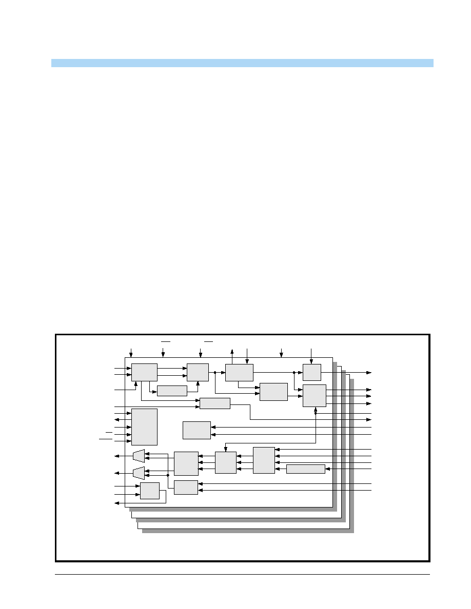
GENERAL DESCRIPTION
The XRT73L03 is a 3-Channel, E3/DS3/STS-1 Line
Interface Unit designed for E3, DS3 or SONET STS-1
applications and consists of three independent line
transmitters and receivers integrated on a single chip.
Each channel of the XRT73L03 can be configured to
support the E3 (34.368 Mbps), DS3 (44.736 Mbps) or
the SONET STS-1 (51.84 Mbps) rates. Each channel
can be configured to operate in a mode/data rate that
is independent of the other channels.
In the transmit direction, each channel in the
XRT73L03 encodes input data to either B3ZS or
HDB3 format and converts the data into the appropri-
ate pulse shapes for transmission over coaxial cable
via a 1:1 transformer.
In the receive direction, the XRT73L03 can perform
Equalization on incoming signals, perform Clock Re-
covery, decode data from either B3ZS or HDB3 for-
mat, convert the receive data into TTL/CMOS format,
check for LOS or LOL conditions and detect and de-
clare the occurrence of Line Code Violations.
APPLICATIONS
· Digital Cross Connect Systems
· CSU/DSU Equipment
· Routers
· Fiber Optic Terminals
· Multiplexers
· ATM Switches
FEATURES
· Meets E3/DS3/STS-1 Jitter Tolerance Require-
ments
· Full Loop-Back Capability
· Transmit and Receive Power Down Modes
· Full Redundancy Support
· Contains a 4-Wire Microprocessor Serial Interface
· Uses Minimum External components
· Single +3.3V Power Supply
· 5V tolerant I/O
· -40°C to +85°C Operating Temperature Range
· Available in a Thermally Enhanced 120 pin TQFP
package
F
IGURE
1. XRT73L03 B
LOCK
D
IAGRAM
ENDECDIS
RLOS(n)
LLB(n)
RLB(n)
TAOS(n)
TPData(n)
TNData(n)
TxClk(n)
TxLEV(n)
TxOFF(n)
Channel 3 - (n) = 3
A G C /
Equalizer
Serial
Processor
Interface
Peak
Detector
LOS Detector
Slicer
Clock
R e c o v e r y
Data
R e c o v e r y
Invert
L o o p M U X
H D B 3 /
B 3 Z S
D e c o d e r
L O S T H R ( n )
SDI
S D O
SClk
C S
R E G R
RTIP(n)
RRing(n)
REQEN(n)
Channel 1 - (n) = 1
Channel 2 - (n) = 2
Notes: 1. (n) = 1, 2 or 3 for respective Channels
2. Serial Processor Interface input pins are shared by the three Channels in HOST Mode and redefined in Hardware Mo de.
Device
Monitor
MTIP(n)
MRing(n)
D M O ( n )
Transmit
Logic
Duty Cycle Adjust
TTIP(n)
TRing(n)
Pulse
Shaping
H D B 3 /
B 3 Z S
Encoder
E3_Ch(n)
STS-1/DS3_Ch(n)
Host/(HW)
RLOL(n)
EXClk(n)
R x O F F
RxClkINV
RxClk(n)
RPOS(n)
RNEG(n)
LCV(n)
Tx
Control

XRT73L03
3 CHANNEL E3/DS3/STS-1 LINE INTERFACE UNIT
áç
áç
áç
áç
PRELIMINARY
REV. P1.0.13
2
TRANSMIT INTERFACE CHARACTERISTICS
· Accepts either Single-Rail or Dual-Rail data from
Terminal Equipment and generates a bipolar signal
from the line
· Integrated Pulse Shaping Circuit.
· Built-in B3ZS/HDB3 Encoder (which can be dis-
abled)
· Contains Transmit Clock Duty Cycle Correction Cir-
cuit on-chip
· Generates pulses that comply with the ITU-T G.703
pulse template for E3 applications
· Generates pulses that comply with the DSX-3 pulse
template, as specified in Bellcore GR-499
-CORE
and ANSI T1.102_1993
· Generates pulses that comply with the STSX-1
pulse template, as specified in Bellcore GR-253-
CORE
· Transmitter can be turned off in order to support
redundancy designs
RECEIVE INTERFACE CHARACTERISTICS
· Integrated Adaptive Receive Equalization (optional)
and Timing Recovery
· Declares and Clears the LOS defect per ITU-T
G.775 requirements for E3 and DS3 applications
· Meets Jitter Tolerance Requirements, as specified
in ITU-T G.823_1993 for E3 Applications
· Meets Jitter Tolerance Requirements, as specified
in Bellcore GR-499-CORE for DS3 Applications
· Declares Loss of Signal (LOS) and Loss of Lock
(LOL) Alarms
· Built-in B3ZS/HDB3 Decoder (which can be dis-
abled)
· Recovered Data can be muted while the LOS Con-
dition is declared
· Outputs either Single-Rail or Dual-Rail data to the
Terminal Equipment
· Receiver can be powered down in order to con-
serve power in redundancy designs
áç
áç
áç
áç
3 CHANNEL E3/DS3/STS-1 LINE INTERFACE UNIT
XRT73L03
PRELIMINARY
REV. P1.0.13
3
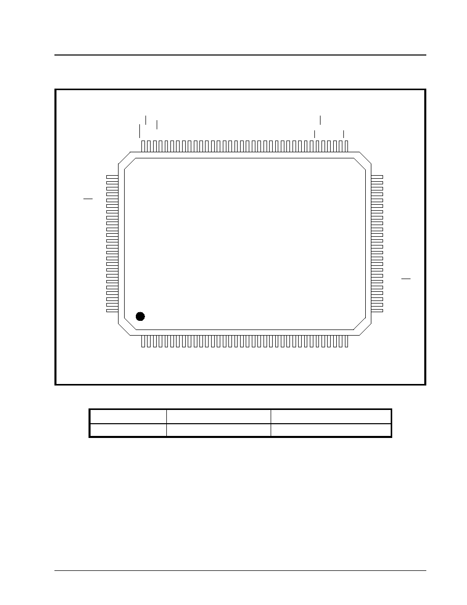
ORDERING INFORMATION
F
IGURE
2. P
IN
OUT
OF
THE
XRT73L03
IN
THE
14
X
20
MM
, 0.5
MM
PITCH
TQFP
1
2
3
4
5
6
7
8
9
10
11
12
13
14
15
16
17
18
19
20
21
22
23
24
25
26
27
28
29
30
31
32
33
34
35
36
96
95
94
93
92
91
90
89
88
87
86
85
84
83
82
81
80
79
78
77
76
75
74
73
72
71
70
69
68
67
66
65
64
63
62
61
9 7
9 8
9 9
1 0 0
1 0 1
1 0 2
1 0 3
1 0 4
1 0 5
1 0 6
1 0 7
1 0 8
1 0 9
1 1 0
1 1 1
1 1 2
1 1 3
1 1 4
1 1 5
1 1 6
1 1 7
1 1 8
1 1 9
1 2 0
6 0
5 9
5 8
5 7
5 6
5 5
5 4
5 3
5 2
5 1
5 0
4 9
4 8
4 7
4 6
4 5
4 4
4 3
4 2
4 1
4 0
3 9
3 8
3 7
XRT73L03
RLOL3
LCV3
RLOS3
RLOL1
LCV1
RLOS1
RxDGND1
NC
NC
RPOS1
RNEG1
RxClk1
RxDVDD1
EXClk1
RxDGND3
RPOS3
RNEG3
RxClk3
HOST/(HW)
RxDVDD3
AGND1
TxAGND1
DMO1
TxAVDD1
REGR/(RxClkINV)
STS1/DS3_Ch2
AGND3
SR/(DR)
E3_CH2
NC
NC
LOSTHR2
LLB2
RLB2
RxAVDD2
RRing2
RTIP2
RxAGND2
REQEN2
RxAGND3
RTIP3
RRing3
RxAVDD3
RLB3
LLB3
LOSTHR3
REQEN1
RxAGND1
RTIP1
RRing1
RxAVDD1
RLB1
LLB1
LOSTHR1
ICT
STS1/DS3_Ch1
SDO/(E3_Ch1)
SDI/(RxOFF1)
SClk/(RxOFF2)
CS/(ENDECDIS)
TNData2
TPData2
TxClk2
MRing2
MTIP2
TAOS2
TAOS3
TxLev2
TxLev3
TTIP2
TxAVDD2
TRing2
TxAGND2
TxAGND3
MRing3
MTIP3
TxAGND3
TRing3
TxAVDD3
TTIP3
DMO3
TxAVDD3
TNData3
TPData3
TxClk3
TxAGND1
TRing1
TxAVDD1
TTIP1
MTIP1
MRing1
TNData1
TPData1
TxClk1
TxLEV1
TAOS1
E X D G N D
E X D V D D
E X C l k 2
R E Q E N 3
S T S 1 / D S 3 _ C h 3
E 3 _ C H 3
E X C l k 3
R x O F F 3
R L O L 2
L C V 2
R L O S 2
R x D G N D 2
R P O S 2
R N E G 2
R x C l k 2
L O S M U T E N
R x D V D D 2
A G N D 2
T x O F F 3
T x O F F 2
T x O F F 1
T x A G N D 2
T x A V D D 2
D M O 2
P
ART
#
P
ACKAGE
O
PERATING
TEMPERATURE
R
ANGE
XRT73L03IV
120 Pin TQFP 14mm X 20mm
-40
o
C to +85
o
C

XRT73L03
3 CHANNEL E3/DS3/STS-1 LINE INTERFACE UNIT
áç
áç
áç
áç
PRELIMINARY
REV. P1.0.13
I
GENERAL DESCRIPTION ................................................................................................. 1
APPLICATIONS ......................................................................................................................................... 1
F
EATURES
.................................................................................................................................................... 1
Figure 1. XRT73L03 Block Diagram ................................................................................................................. 1
T
RANSMIT
I
NTERFACE
C
HARACTERISTICS
...................................................................................................... 2
R
ECEIVE
I
NTERFACE
C
HARACTERISTICS
........................................................................................................ 2
Figure 2. Pin out of the XRT73L03 in the 14 x 20mm, 0.5mm pitch tqfp .......................................................... 3
ORDERING INFORMATION ............................................................................................... 3
PIN DESCRIPTIONS .......................................................................................................... 4
ELECTRICAL CHARACTERISTICS ................................................................................ 15
Figure 3. Transmit Pulse Amplitude Test Circuit for E3, DS3 and STS-1 Rates (typical channel) ................. 17
Figure 4. Timing Diagram of the Transmit Terminal Input Interface ................................................................ 17
Figure 5. Timing Diagram of the Receive Terminal Output Interface .............................................................. 17
A
BSOLUTE
M
AXIMUM
R
ATINGS
....................................................................................................... 21
Figure 6. Microprocessor Serial Interface Data Structure ............................................................................... 22
Figure 7. Timing Diagram for the Microprocessor Serial Interface .................................................................. 22
SYSTEM DESCRIPTION .................................................................................................. 23
T
HE
T
RANSMIT
S
ECTION
- C
HANNELS
1, 2
AND
3 ......................................................................................... 23
T
HE
R
ECEIVE
S
ECTION
- C
HANNELS
1, 2
AND
3 ........................................................................................... 23
T
HE
M
ICROPROCESSOR
S
ERIAL
I
NTERFACE
................................................................................................. 23
T
ABLE
1: R
OLE
OF
M
ICROPROCESSOR
S
ERIAL
I
NTERFACE
PINS
WHEN
THE
XRT73L03
IS
OPERATING
IN
THE
H
ARD
-
WARE
M
ODE
....................................................................................................................................... 23
Figure 8. Functional Block Diagram of the XRT73L03 .................................................................................... 24
1.0 Selecting the Data Rate .................................................................................................................... 24
1.1 C
ONFIGURING
C
HANNEL
(
N
) .............................................................................................................................. 24
T
ABLE
2: A
DDRESSES
AND
B
IT
F
ORMATS
OF
XRT73L03 C
OMMAND
R
EGISTERS
................................................. 24
T
ABLE
3: S
ELECTING
THE
D
ATA
R
ATE
FOR
C
HANNEL
(
N
)
OF
THE
XRT73L03,
VIA
THE
E3_C
H
(
N
)
AND
STS-1/
DS3_C
H
(
N
)
INPUT
PINS
(H
ARDWARE
M
ODE
) ....................................................................................... 26
2.0 The Transmit Section ....................................................................................................................... 26
C
OMMAND
R
EGISTER
CR4-(
N
) ...................................................................................................... 26
T
ABLE
4: S
ELECTING
THE
D
ATA
R
ATE
FOR
C
HANNEL
(
N
)
OF
THE
XRT73L03
VIA
THE
STS-1/DS3_C
H
(
N
)
AND
THE
E3_C
H
(
N
)
BIT
-
FIELDS
IN
THE
A
PPROPRIATE
C
OMMAND
R
EGISTER
(HOST M
ODE
) ................................ 26
2.1 T
HE
T
RANSMIT
L
OGIC
B
LOCK
........................................................................................................................... 26
2.1.1 Accepting Dual-Rail Data from the Terminal Equipment ................................................................ 26
Figure 9. The typical interface for Data Transmission in Dual-Rail Format from the Transmitting Terminal Equip-
ment to the Transmit Section of a channel of the XRT73L03 ....................................................... 27
Figure 10. How the XRT73L03 Samples the data on the TPData and TNData input pins .............................. 27
2.1.2 Configure Channel(n) to accept Single-Rail Data from the Terminal Equipment ........................ 27
C
OMMAND
R
EGISTER
CR1-(
N
) ....................................................................................................... 27
Figure 11. The Behavior of the TPData and TxClk Input Signals while the Transmit Logic Block is Accepting
Single-Rail Data from the Terminal Equipment ............................................................................. 28
2.2 T
HE
T
RANSMIT
C
LOCK
D
UTY
C
YCLE
A
DJUST
C
IRCUITRY
.................................................................................. 28
2.3 T
HE
HDB3/B3ZS E
NCODER
B
LOCK
................................................................................................................. 28
2.3.1 B3ZS Encoding ................................................................................................................................... 28
Figure 12. An Example of B3ZS Encoding ..................................................................................................... 29
2.3.2 HDB3 Encoding .................................................................................................................................. 29
Figure 13. An Example of HDB3 Encoding ..................................................................................................... 29
2.3.3 Disabling the HDB3/B3ZS Encoder .................................................................................................. 29
C
OMMAND
R
EGISTER
CR2-(
N
) ....................................................................................................... 30
2.4 T
HE
T
RANSMIT
P
ULSE
S
HAPING
C
IRCUITRY
...................................................................................................... 30
Figure 14. The Bellcore GR-499-CORE Transmit Output Pulse Template for DS3 Applications ................... 30
Figure 15. The Bellcore GR-253-CORE Transmit Output Pulse Template for SONET STS-1 Applications ... 31
2.4.1 Enabling the Transmit Line Build-Out Circuit ................................................................................. 31
C
OMMAND
R
EGISTER
CR1-(
N
) ....................................................................................................... 31
2.4.2 Disabling the Transmit Line Build-Out Circuit ................................................................................ 31

áç
áç
áç
áç
3 CHANNEL E3/DS3/STS-1 LINE INTERFACE UNIT
XRT73L03
PRELIMINARY
REV. P1.0.13
II
C
OMMAND
R
EGISTER
CR1-(
N
) ...................................................................................................... 32
2.4.3 Design Guideline for Setting the Transmit Line Build-Out Circuit ................................................ 32
2.4.4 The Transmit Line Build-Out Circuit and E3 Applications ............................................................. 32
2.5 I
NTERFACING
THE
T
RANSMIT
S
ECTIONS
OF
THE
XRT73L03
TO
THE
L
INE
.......................................................... 32
Figure 16. Recommended Schematic for Interfacing the Transmit Section of the XRT73L03 to the Line ..... 32
TRANSFORMER VENDOR INFORMATION ........................................................................................... 33
3.0 The Receive Section ........................................................................................................................ 33
3.1 I
NTERFACING
THE
R
ECEIVE
S
ECTIONS
OF
THE
XRT73L03
TO
THE
L
INE
............................................................ 33
Figure 17. Recommended Schematic for Transformer-Coupling the Receive Section of the XRT73L03 to the
Line ............................................................................................................................................... 34
Figure 18. Recommended Schematic for Capacitive-Coupling the Receive Section of the XRT73L03 to the Line
....................................................................................................................................................... 34
3.2 T
HE
R
ECEIVE
E
QUALIZER
B
LOCK
..................................................................................................................... 35
Figure 19. The Typical Application for the System Installer ........................................................................... 35
C
OMMAND
R
EGISTER
CR2_(
N
) ...................................................................................................... 36
3.3 C
LOCK
R
ECOVERY
PLL ................................................................................................................................... 36
3.3.1 The Training Mode ............................................................................................................................. 36
3.3.2 The Data/Clock Recovery Mode ....................................................................................................... 36
3.4 T
HE
HDB3/B3ZS D
ECODER
............................................................................................................................ 36
3.4.1 B3ZS Decoding DS3/STS-1 Applications ......................................................................................... 36
Figure 20. An Example of B3ZS Decoding ..................................................................................................... 37
3.4.2 HDB3 Decoding E3 Applications ...................................................................................................... 37
Figure 21. An Example of HDB3 Decoding .................................................................................................... 37
3.4.3 Configuring the HDB3/B3ZS Decoder .............................................................................................. 37
C
OMMAND
R
EGISTER
CR2-(
N
) ...................................................................................................... 38
3.5 LOS D
ECLARATION
/C
LEARANCE
...................................................................................................................... 38
3.5.1 The LOS Declaration/Clearance Criteria for E3 Applications ........................................................ 38
Figure 22. The Signal Levels at which the XRT73L03 declares and clears LOS ........................................... 39
Figure 23. The Behavior the LOS Output Indicator in response to the Loss of Signal and the Restoration of Sig-
nal ................................................................................................................................................. 39
3.5.2 The LOS Declaration/Clearance Criteria for DS3 and STS-1 Applications ................................... 40
T
ABLE
5: T
HE
ALOS (A
NALOG
LOS) D
ECLARATION
AND
C
LEARANCE
T
HRESHOLDS
FOR
A
GIVEN
SETTING
OF
LOSTHR
AND
REQEN
FOR
DS3
AND
STS-1 A
PPLICATIONS
.............................................................. 40
C
OMMAND
R
EGISTER
CR0-(
N
) ...................................................................................................... 40
C
OMMAND
R
EGISTER
CR2-(
N
) ...................................................................................................... 41
C
OMMAND
R
EGISTER
CR0-(
N
) ...................................................................................................... 41
C
OMMAND
R
EGISTER
CR2-(
N
) ...................................................................................................... 41
3.5.3 Muting the Recovered Data while the LOS is being Declared ....................................................... 41
C
OMMAND
R
EGISTER
CR3-(
N
) ...................................................................................................... 42
3.6 R
OUTING
THE
R
ECOVERED
T
IMING
AND
D
ATA
I
NFORMATION
TO
THE
R
ECEIVING
T
ERMINAL
E
QUIPMENT
............. 42
3.6.1 Routing Dual-Rail Format Data to the Receiving Terminal Equipment ......................................... 42
Figure 24. The typical interface for the Transmission of Data in a Dual-Rail Format from the Receive Section of
the XRT73L03 to the Receiving Terminal Equipment .................................................................. 42
Figure 25. How the XRT73L03 outputs data on the RPOS and RNEG output pins ....................................... 43
Figure 26. The Behavior of the RPOS, RNEG and RxClk signals when RxClk is inverted ............................ 43
C
OMMAND
R
EGISTER
CR3-(
N
) ...................................................................................................... 44
3.6.2 Routing Single-Rail Format (Binary Data Stream) data to the Receive Terminal Equipment ..... 44
C
OMMAND
R
EGISTER
CR3-(
N
) ...................................................................................................... 44
Figure 27. The typical interface for Data Transmission in a Single-Rail Format from the Receive Section of the
XRT73L03 to the Receiving Terminal Equipment ........................................................................ 44
Figure 28. The behavior of the RPOS and RxClk output signals while the XRT73L03 is transmitting Single-Rail
data to the Receiving Terminal Equipment .................................................................................. 45
3.7 S
HUTTING
OFF
THE
R
ECEIVE
S
ECTION
............................................................................................................. 45
C
OMMAND
R
EGISTER
CR3-(
N
) ...................................................................................................... 45
4.0 Diagnostic Features of the XRT73L03 ............................................................................................ 46
4.1 T
HE
A
NALOG
L
OCAL
L
OOP
-B
ACK
M
ODE
.......................................................................................................... 46
Document Outline