
XR-T56L22
...the analog plus company
TM
Low Power
Repeater/Receiver
Rev. 1.02
E
1997
EXAR Corporation, 48720 Kato Road, Fremont, CA 94538
z
(510) 668-7000
z
FAX (510) 668-7017
1
June 1997-3
FEATURES
D
Contains All The Active Components For A PCM
Repeater Or Long Haul Line Receiver
D
Low Voltage Operation (5.1V)
D
Low Power Consumption (8.75mA Max)
D
2Mbps Operation Capability
D
Dual Matched ALBO Ports
D
Internal Adjustable Phase Shift Circuitry
D
Extracted Clock Output
D
Internal Shunt Regulator
D
Temperature Independent Current Biasing
APPLICATIONS
D
T1 PCM Repeater/Receiver
D
T148C PCM Repeater/Receiver
D
European 2.048Mbps PCM Repeater/Receiver
D
Digital Multiplexers, CSUs, Switching Equipment
D
ISDN Compatible Equipment: Fax Machines,
Computers etc.
GENERAL DESCRIPTION
The XR-T56L22 is a very low power monolithic repeater/
receiver IC designed for PCM carrier systems operating
between 1.544Mbps and 2.37Mbps. The IC provides all
the active circuitry required to implement one side of a
PCM repeater. The XR-T56L22 features on-chip
adjustable phase shifting, an extracted clock output and
an on-board shunt regulator. The very low power
consumption of the device makes it ideal for long haul
"tandem" repeater applications.
ORDERING INFORMATION
Part No.
Package
Operating
Temperature Range
XR-T56L22AP
18 Lead 300 Mil PDIP
-40
�
C to +85
�
C
XR-T56L22AN
18 Lead 300 Mil CDIP
-40
�
C to +85
�
C
XR-T56L22AD
18 Lead 300 Mil Jedec SOIC
-40
�
C to +85
�
C

XR-T56L22
2
Rev. 1.02
BLOCK DIAGRAM
ALBO1
ALBO2
ANA GND
AMP + I/P
AMP - I/P
LC I/P
REG Cont.
V
CC
DIG GND
LC Bias
Phase Cont.
2
3
1
5
4
+
-
16
17
15
13
14
12
8
+5
18
6
7
11
9
10
ALBO FIL
AMP -O/P
AMP +O/P
Clock O/P
Data +
Data -
ALBO
PEAK
DET.
AMP
Clock
Comparators
Clock
Bias
GEN.
Clock
AMP
Clock
Driver
Data
Comparators
D
CLK
Q
Data
Latches
Output
Drivers
D
CLK
Q
Voltage
Ref.
Gen.
Volt.
Reg.
Figure 1. XT-T56L22 Block Diagram
V
REF
XR-T56L22
3
Rev. 1.02
PIN CONFIGURATION
1
2
3
4
5
6
7
8
9
18
17
16
15
14
13
12
11
10
ALBO FIL
LC BIAS
LC I/P
PHASE CONT.
REG CONT.
V
REF
V
CC
CLOCK O/P
ANA GND
ALBO1
ALBO2
AMP-I/P
AMP +I/P
AMP -O/P
AMP +O/P
DIG GND
DATA-
DATA+
18 Lead PDIP, CDIP (0.300")
18
1
10
9
2
3
4
5
6
7
15
14
13
12
11
17
16
8
ALBO FIL
LC BIAS
LC I/P
PHASE CONT.
ANA GND
ALBO1
ALBO2
AMP-I/P
REG CONT.
VREF
V
CC
CLOCK O/P
AMP +I/P
AMP -O/P
AMP +O/P
DIG GND
DATA-
DATA+
18 Lead SOIC (Jedec, 0.300")
PIN DESCRIPTION
Pin #
Symbol
Description
1
ANA GND
Ground for Analog Sections of IC and Substrate.
2
ALBO 1
ALBO PORT 1 Output. Port impedance varies between 25W and 20kW proportional to input signal
level.
3
ALBO 2
ALBO PORT 2 Output. Similar to pin 2.
4
AMP - I/P
Inverting Input of Signal Preamp RIN > 20kW.
5
AMP + I/P
Non-Inverting Input of Signal Preamp. RIN > 20kW.
6
AMP - O/P
Inverting Output of Signal Pre-amp. Rout < 200W. DC level typically 3.2V.
7
AMP + O/P
Non-inverting Output of Signal Pre-amp. Similar to pin 6.
8
DIG GND
Ground for Digital Portion of IC.
9
DATA+
Positive Data Driver Output (Open Collector). V
OL
< 0.95V @ l
OUT
= 32mA.
10
DATA-
Negative Data Driver Output (Open Collector). V
OL
< 0.95V @ l
OUT
= 32mA.
11
CLOCK O/P
Phase Shifted Clock Output (Open Collector). Decouple to GND with 0.1mF if not required. With
Rpull-up = 1K, V
OL
< 1.1V @ I
OUT
= 4mA.
12
V
CC
Input Pin of Shunt Regulator and Supply Pin for IC. For voltage feed applications the regulator
must be disabled and a 5V + 5% supply connected. For line feed a current of 48-120mA is required.
ICC < 8.75mA @ RON, ALBO = 25W typical.
13
VREF
Output Voltage of Internal Reference of Shunt Regulator. For parallel operation of regulators
should be tied to pin 13 of 2nd T56L22 device. V
REF
approxi-mately V
CC
/2. Decouple to GND with
0.1mF.
14
REG CONT
Input Voltage of Shunt Regulator Amp. To inhibit regulator, pin should be tied to ground. For line
feed operation decouple to GND with 0.1mF. For parallel operation of regulators tie pin 14 of 2nd
T56L22 device. VREG approximately V
REF
.
15
PHASE
CONT
Phase Shift Adjust Input. A resistor to GND from the pin allows adjustment of phase shift from 905
to approximately 05. RP typical 1.8K to 1K. Vphase typical 340mV.
16
LC I/P
Clock Amplifier Input. Pulsed with current from clock comparator. Connect LC tank between 16, 17
for clock recovery. Ickon = --110mA typical.
17
LC BIAS
Clock Amplifier Reference Voltage. VLC = 3.6V typical.
18
ALBO FIL
Control Pin for ALBO Ports. Voltage developed across a capacitor on this pin defines ALBO on
impedance VALBO = 1.5V typical.
XR-T56L22
4
Rev. 1.02
ELECTRICAL CHARACTERISTICS
Test Conditions: TA = -40
�
C to
+
85
�
C, V
CC
= 5.1V
�
5% unless otherwise specified - refer to test circuit (Figure 6).
Parameter
Pin
Min.
Typ.
Max.
Unit
Conditions
General
Supply Voltage
12
4.85
5.35
V
Pin 12, 13 to V
CC
1
Supply Current
12
7
8.75
mA
Data Output Leakage Current
9, 10
100
m
A
V
pull-up
= 8V
ALBO Port Off Voltage
2, 3
0.1
V
V
CC
= 5.35 V
1
Amplifier Pin Voltage
4, 5
2.7
3.2
3.7
V
Amplifier Pin Voltage
6, 7
Amplifier
Input Impedance
4, 5
40
K
W
Input Offset Voltage
4, 5
-10
10
mV
R
S
= 8.2K
2
Input Bias Current
4, 5
5
m
A
R
S
= 8.2K
2
Input Offset Current
4, 5
-1
1
mV
R
S
= 8.2K
2
Output Offset Voltage
6, 7
-50
50
W
R
S
= 8.2K
2
Common Mode Rejection Ratio
4, 5, 6, 7
40
dB
Output Volage Swing
6, 7
1.9
V
Clock Amplifier
Input Offset Voltage
17, 16
0.5
6
mV
R
S
= 10K
3
Input Bias Current
17, 16
5
m
A
4
AC Gain
40
dB
-3db bandwidth
10
MHz
Delay
35
ns
ALBO
ALBO Filter Resistance
18-1
31
57
K
W
ALBO Impedance Match
2, 3
10
%
On Current
1
1.3
2.4
mA
Drive Current
18
0.4
1.4
mA
Maximum On Impedance
2, 3-1
25
W
5
Minimum Off Inpedance
2, 3-1
20
KW
5
Notes
1
Internal regulator disabled.
2
Source Resistance.
3
R
S
= Wou4d3 43wiw5qnd3 PIN 16 positive with respect to Pin 17
4
Pin 16 = Pin 17 = 3.6V
5
f
test
= 1MHz
Specifications are subject to change without notice
XR-T56L22
5
Rev. 1.02
ELECTRICAL CHARACTERISTICS
(CON'T)
Parameter
Pin
Min.
Typ.
Max.
Unit
Conditions
Threshold Voltages
ALBO Threshold +Ve
7, 6
1.4
1.6
V
1, 2
ALBO Threshold -Ve
7, 6
1.4
1.6
V
1, 2
ALBO Threshold Difference
-3
3
%
3
Clock Drive on Current + Ve
80
140
m
A
4
Clock Drive on Current -Ve
80
140
m
A
4
Clock Drive Difference
-3
3
%
3
Clock Threshold +Ve
7, 6
69
79
%
5
Clock Threshold -Ve
7, 6
69
79
%
5
Clock Threshold Difference
-3
3
%
3
Data Threshold +Ve
7, 6
41
50
%
3
Data Threshold -Ve
7, 6
41
50
%
5
Data Threshold Difference
-3
3
%
3
Data Output Stages
Output Pulse Rise Time + Ve (Tr)
9
40
nS
10%-90%
6
Output Pulse Rise -Time-Ve(Tr)
10
40
nS
10%-90%
6
Output Pulse Fall Time+Ve(Tf)
9
40
nS
10%-90%
6
Output Pulse Fall Time -Ve (Tf)
10
40
nS
10%-90%
6
Output Pulse Width +Ve (Tw)
9
224
264
nS
at 50%
Output Pulse Width -Ve (Tw)
10
224
264
nS
at 50%
Output Pulse Width Difference
(dTw)
-12
12
nS
at 50%
Output Voltage (low) (V
OL
)
9, 10
0.6
0.95
V
6
Output Voltage Difference (V
OL
)
9, 10
-0.15
0.15
V
6
Notes
1
Pk/pk voltage at Pins 6 and 7 of a 1MHz sine wave derived through amplifier and measured differentially.
2
Pk/pk voltage at Pins 6 and 7 adjusted for a current increase of 2mA at pin 1.
3
Calculation only: percentage difference = [higher value/lower value]-1 x 100%.
4
V
6
- V
7
adjusted to ALBO threshold voltage (Pin 16 = 3.6V)
5
Figure taken as a percentage of ALBO threshold.
6
Using a 130
W
pull up resistor between 9, 10 and V
CC
and 15pF capacitance to GND.
Specifications are subject to change without notice
XR-T56L22
6
Rev. 1.02
ELECTRICAL CHARACTERISTICS
(CONT'D)
Parameter
Pin
Min.
Typ.
Max.
Unit
Conditions
Clock Output Stage
Output Pulse Rise Time (Tr)
11
40
ns
1
Output Pulse Fall Time (Tf)
11
40
ns
Output Pulse Width (Tw)
11
224
264
ns
Shunt Regulator
Output Voltage
12
4.85
5.1
5.35
V
Pin 13, 14 floating
Voltage Regulation Over Temp.
12
-0.02
%/
�
C
Pin 13, 14 floating
Load Regulation
12
0.027
%/mA
1mA to 100mA load
Note
1
Using a 2K pull up resistor between 11 and V
CC
and 15pF capacitance to GND.
ABSOLUTE MAXIMUM RATINGS
Storage Temperature
-65
�
C to 150
�
C
. . . . . . . . . . . . . .
Operating Temperature
-40
�
C to 85
�
C
. . . . . . . . . . . . .
Supply Voltage
-0.5 to 7V
. . . . . . . . . . . . . . . . . . . . . . . .
Supply Voltage Surge (10ms)
25V
. . . . . . . . . . . . . . . . .
Data Output Voltage (pin 9, 10)
12V
. . . . . . . . . . . . . . .
SYSTEM DESCRIPTION
With reference to the functional block diagram, the basic
operation of the XR-T56L22 may be described as follows:
The received bipolar signal, is applied to a linear amplifier
and automatic equalizer. These circuits provide the
necessary amount of gain and phase equalization to
recover the transmitted data, and band limit the signal, to
optimize repeater performance for near-end crosstalk
produced by other systems operating within the same
cable bundle.
The preamplifier output signals which are balanced and of
opposite phase, are applied to the clock extraction and
pulse regenerator circuits. Here they are rectified and
then applied to a high Q resonant circuit which extracts
the 1.544/2.048 Mbps frequency component from the
received signal. This signal is then sliced and fed to an
adjustable phase shift circuit. A second slicer is used to
control the time at which the output signals from the
preamplifier are sampled by the pulse regenerator
circuits. The phase shifted clock signal is made available
as an output from the circuit for interface applications. The
clock phase adjustment is performed with a single pin
using an external resistor. Adjustment of the position of
the clock sampling edge by the phase shift circuit allows
performance of the pulse regenerator to be optimized.
The pulse regenerator performs the sampling and data
slicing to regenerate the appropriate output pulse. These
pulses are applied to an external output transformer to
create the bipolar signal that drives the next section of
twisted pair.
XR-T56L22
7
Rev. 1.02
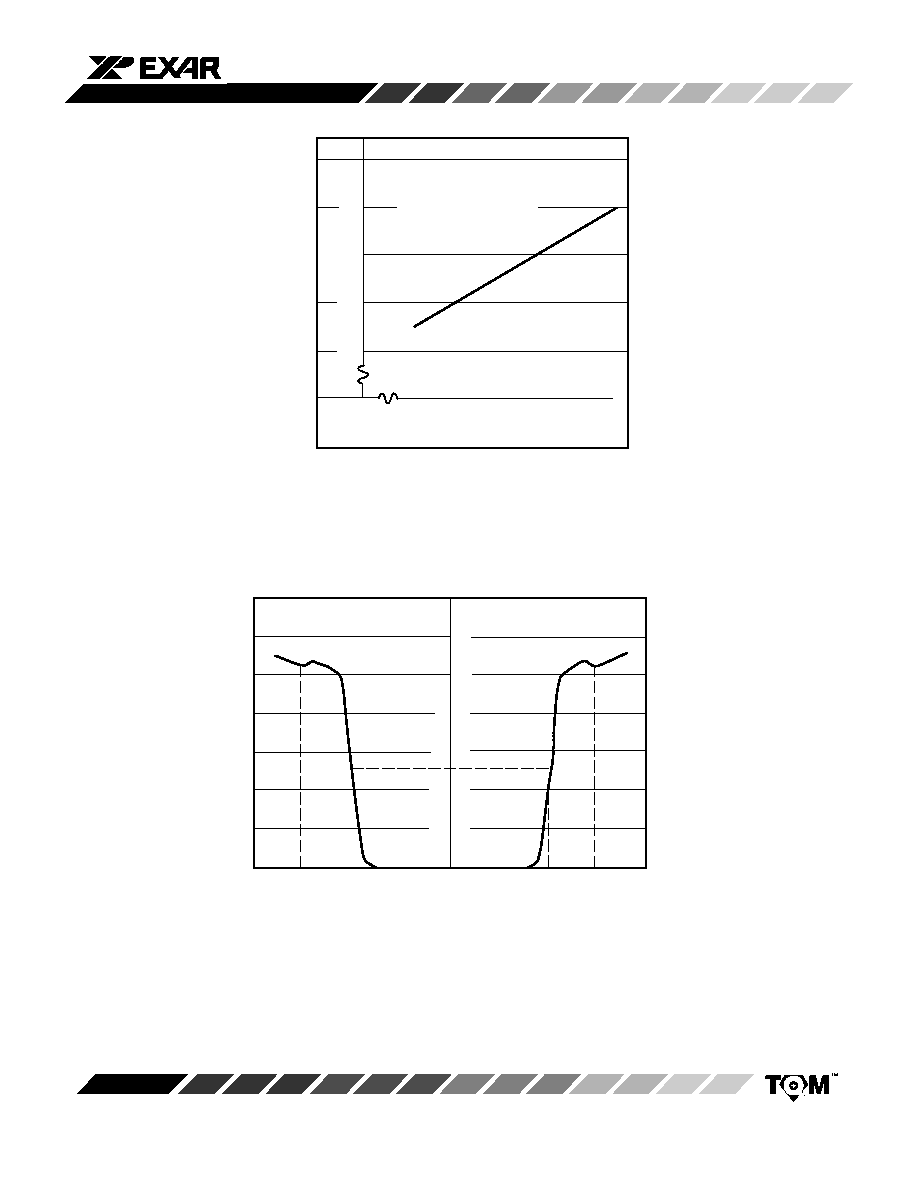
Figure 2. Supply Current Variation
with V
CC
(Regulator Inhibited)
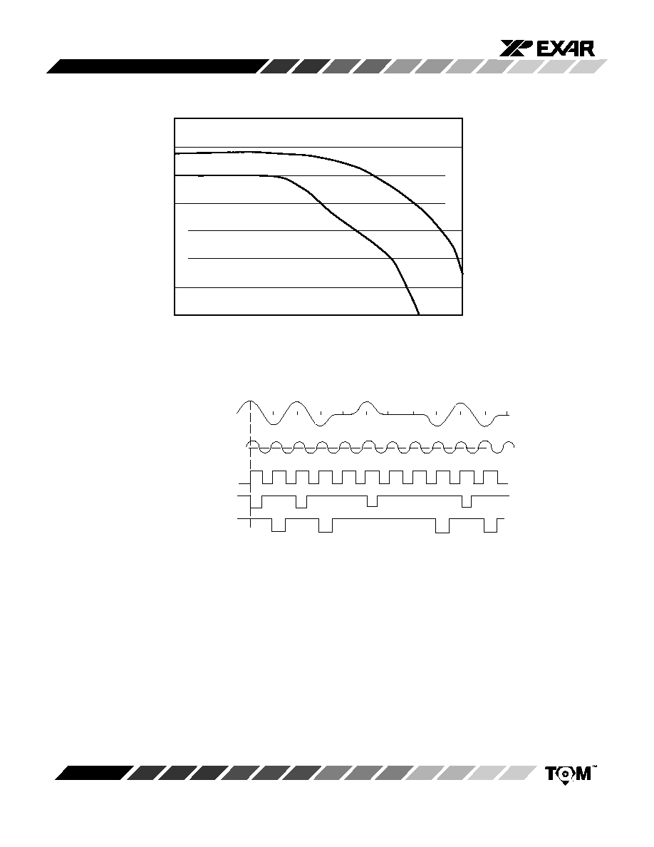
Figure 3. Clock Drive Current Against Preamp Output Voltage
Typical I
CC
Vs. V
CC
Variation at T=25
�
C
(Clock, Data Outputs
(V
IN
=6V p-p (@2.04MBPS)
+ ALBO all Operating)
4.7
4.8
4.9
5.0
5.1
5.2
5.3
5.4
5.5
6.4
6.6
6.8
7.0
7.2
7.4
7.6
7.8
V
CC
in Volts
I
CC
in (mA)
Max Clock Drive
Current = 100
m
A
@ Albo Thresholds
50% CLK Drive Max
Clk Drive (
A)
m
1.8
1.6
1.4
1.2
1.0
.8
.6
.4
.2
0
1.8 1.6 1.4 1.2 1.0
.8
.6
.4
.2
10
20
30
40
50
60
70
80
90
100
110
120
V
ALBOTHLD
= 1.44 CLK
V
CLKTHLD
= 1.02v
V
PREAMP
OUT (V)
CLK
THLD(+)
ALBO
THLD(+)
XR-T56L22
8
Rev. 1.02
Figure 4. Typical T56L22 Waveforms
Preamp Output
(Approx. 1.5 pK to pK)
Oscillator Input
Pin 16
Clock Output
Pin 12
Data Pos.
Pin 18
Data Neg.
Pin 1
Figure 5. Preamp Gain/Phase Characteristics
0
�45
�90
�135
�180
10
4
10
5
10
6
10
7
10
8
Frequency In Hertz
Phase
Differential Gain
Gain A
V
IN DS
40
30
20
�40
�30
�20
�10
0
10
50
60
Phase in Degrees

XR-T56L22
9
Rev. 1.02
Figure 6. AC Parameter Test Circuit
1
2
3
4
5
6
7
8
9
18
17
16
15
14
13
12
11
10
IM
R1
3.9K
R2
100
R3
51
C3
1
�
F
1
�
F
R5
100
C2
8.22UF
C1
8.22UF
R4
8.2K
R6
7.5K
R8
130
V
CC
D
+
C4
+
+
C6
47
�
F
C11
15
�
F
R13
51
C18
1
�
F
C7
8.1
�
F
R11
1.8K
C9
8.1
�
F
R9
138
C5
8.22
�
F
C8
8.22
�
F
D- CLK
R18
1K
V
CC
R7
680

XR-T56L22
10
Rev
. 1.02
Figure 8. XR�T56L22 E1 Evaluation Circuit

XR-T56L22
11
Rev
. 1.02
Figure 9. XR�T56L22 T1 Evaluation Circuit
XR-T56L22
12
Rev. 1.02
18 LEAD PLASTIC DUAL-IN-LINE
(300 MIL PDIP)
Rev. 1.00
18
1
10
9
D
e
B
1
A
1
E
1
C
E
A
2
L
B
Seating
Plane
SYMBOL
MIN
MAX
MIN
MAX
INCHES
A
0.145
0.210
3.68
5.33
A
1
0.015
0.070
0.38
1.78
A2
0.115
0.195
2.92
4.95
B
0.014
0.024
0.36
0.56
B
1
0.030
0.070
0.76
1.78
C
0.008
0.014
0.20
0.38
D
0.845
0.925
21.46
23.50
E
0.300
0.325
7.62
8.26
E
1
0.240
0.280
6.10
7.11
e
0.100 BSC
2.54 BSC
e
A
0.300 BSC
7.62 BSC
e
B
0.310
0.430
7.87
10.92
L
0.115
0.160
2.92
4.06
0
�
15
�
0
�
15
�
MILLIMETERS
A
Note: The control dimension is the inch column
e
B
e
A
XR-T56L22
13
Rev. 1.02
A
0.100
0.200
2.54
5.08
A
1
0.015
0.070
0.38
1.78
B
0.014
0.026
0.36
0.66
B
1
0.045
0.065
1.14
1.65
c
0.008
0.018
0.20
0.46
D
0.860
0.960
21.84
24.38
E
1
0.250
0.310
6.35
7.87
E
0.300 BSC
7.62 BSC
e
0.100 BSC
2.54 BSC
L
0.125
0.200
3.18
5.08
0
�
15
�
0
�
15
�
D
B
e
B
1
18 LEAD CERAMIC DUAL-IN-LINE
(300 MIL CDIP)
Rev. 1.00
SYMBOL
MIN
MAX
MIN
MAX
INCHES
MILLIMETERS
18
1
9
10
c
E
1
L
A
1
Seating
Plane
Base
Plane
A
E
Note: The control dimension is the inch column
XR-T56L22
14
Rev. 1.02
SYMBOL
MIN
MAX
MIN
MAX
A
0.093
0.104
2.35
2.65
A
1
0.004
0.012
0.10
0.30
B
0.013
0.020
0.33
0.51
C
0.009
0.013
0.23
0.32
D
0.447
0.463
11.35
11.75
E
0.291
0.299
7.40
7.60
e
0.050 BSC
1.27 BSC
H
0.394
0.419
10.00
10.65
L
0.016
0.050
0.40
1.27
0
�
8
�
0
�
8
�
INCHES
MILLIMETERS
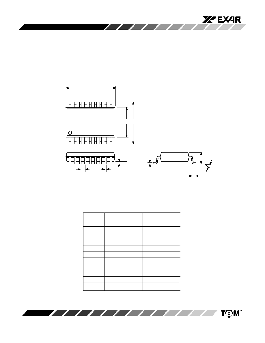
18 LEAD SMALL OUTLINE
(300 MIL JEDEC SOIC)
Rev. 1.00
e
18
10
9
D
E
H
B
A
L
C
A
1
Seating
Plane
Note: The control dimension is the millimeter column
1

XR-T56L22
15
Rev. 1.02
Notes

XR-T56L22
16
Rev. 1.02
NOTICE
EXAR Corporation reserves the right to make changes to the products contained in this publication in order to im-
prove design, performance or reliability. EXAR Corporation assumes no responsibility for the use of any circuits de-
scribed herein, conveys no license under any patent or other right, and makes no representation that the circuits are
free of patent infringement. Charts and schedules contained here in are only for illustration purposes and may vary
depending upon a user's specific application. While the information in this publication has been carefully checked;
no responsibility, however, is assumed for inaccuracies.
EXAR Corporation does not recommend the use of any of its products in life support applications where the failure or
malfunction of the product can reasonably be expected to cause failure of the life support system or to significantly
affect its safety or effectiveness. Products are not authorized for use in such applications unless EXAR Corporation
receives, in writing, assurances to its satisfaction that: (a) the risk of injury or damage has been minimized; (b) the
user assumes all such risks; (c) potential liability of EXAR Corporation is adequately protected under the circum-
stances.
Copyright 1997 EXAR Corporation
Datasheet June 1997
Reproduction, in part or whole, without the prior written consent of EXAR Corporation is prohibited.