
MP7651
1
Rev. 2.00
8-Channel, Voltage Output
10 MHz Input Bandwidth 8-Bit Multiplying
DACs with Serial Digital Data Port
and Chip Select Decoder
FEATURES
·
8 Independent 2-Quadrant Multiplying 8-Bit DACs
·
Serial Digital Input Data and Address Port (3-Wire
Standard) plus Internal Chip Address Decoder
©
·
Dual Supplies (+5 V typ.)
·
High Speed:
12.5 MHz Digital Clock Rate
V
REF
to V
OUT
Settling Time: 150ns to
8-bit (typ)
Voltage Reference Input Bandwidth:
10 MHz (typ)
·
Low Power: 150mW (typ)
·
Low AC Voltage Reference Feedthrough
·
Excellent Channel-to-Channel Isolation
·
DNL = +0.8 LSB, INL = +1 LSB (typ)
·
DACs Matched to +0.5% (typ)
·
Low Harmonic Distortion: 0.25% typical
with V
REF
= 1 V p-p @ 1 MHz
·
V
REF
/2 Output Preset Level
·
Latch-Up Proof
·
Greater than 2000 V ESD Protection
APPLICATIONS
·
ATE
·
Process Control (Low Noise)
·
Convergence Adjustment for High
Resolution Monitors (Work Stations)
·
Digital Gain/Attenuation/Offset Control
·
Trimmer Replacement
GENERAL DESCRIPTION
The MP7651 is ideal for direct gain control of video, compos-
ite video, CCD and other high frequency analog signals. The de-
vice includes 8-channels of high speed, high bandwidth, two
quadrant, multiplying, 8-bit accurate digital-to-analog converter.
It includes an output drive buffer per channel capable of driving
+1mA (typ) to a load. DNL of better than +0.8 LSB is achieved
with a channel-to-channel matching of better than 0.5%. Stabil-
ity, matching, and precision of the DACs is achieved by using
EXAR's thin film technology. Also, excellent channel-to-channel
isolation is achieved with EXAR's BiCMOS process which can-
not be achieved using a typical CMOS technology.
An open loop architecture (patent pending) provides wide
small signal bandwidth from V
REF
to output up to 10 MHz (typ),
fast output settling time, and V
REF
feedthrough isolation of
65dB or better. In addition, low distortion in the order of 0.25%
with a 1 V pp, 1 MHz signal.
A specified and constant input impedance of each V
REF+
in-
put gives flexibility for optimal system design. The serial data
3-wire standard
µ
-processor logic interface reduces pin count,
package size (28 pin), and board wire (space). Additionally, the
internal chip select decoder allows for easy daisy chaining with-
out the addition of separate control logic.
MP7651 is fabricated on a junction isolated, high speed, dual
metal, linear compatible BiCMOS (BiCMOS IV
TM
) thin film resis-
tors. This process enables precision high speed analog/digital
(mixed-mode) circuits to be fabricated on the same chip.

MP7651
2
Rev. 2.00
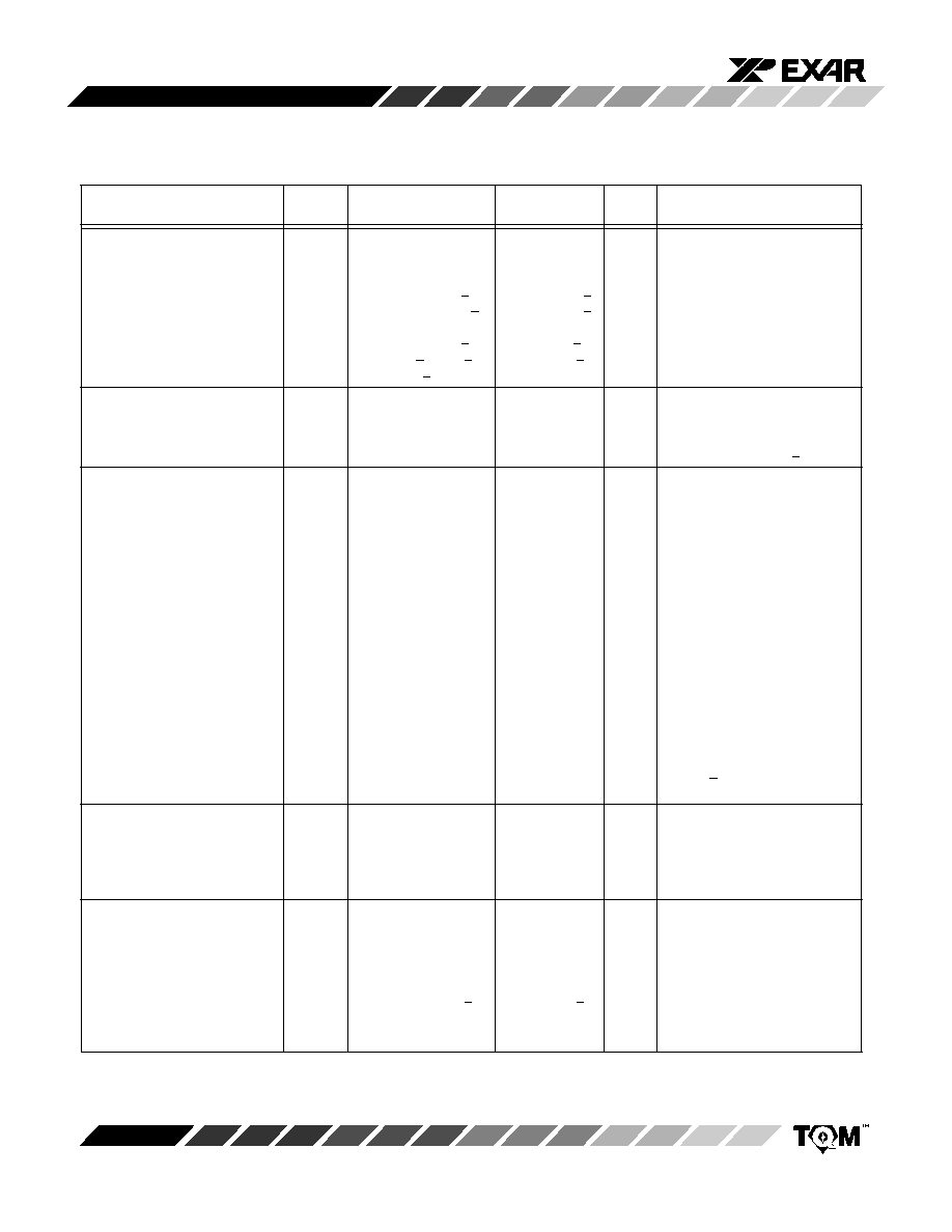
SIMPLIFIED BLOCK DIAGRAM
©
GND
SDO
CLK
RST
1-Bit
Latch
SDI
16-Bit Shift Register
DB0 to DB7
4-Bit CH
Address
LD
8
V
EE
V
CC
V
O0
V
O7
DAC 0
DAC 7
DAC 1
8-Bit Latch
8-Bit Latch
8-Bit Latch
4-8 DEC
8
8
8
8
3-State
Buffer
V
O1
8
4
+1
+1
+1
LD
4-Bit CS
Address
COMP
4
CS0P to
CS3P
4
1-Bit
Latch
8
V
R0
V
R1
V
R7
LD
LD
ORDERING INFORMATION
Package
Type
Temperature
Range
Part No.
SOIC
40 to +85
°
C
MP7651AS
+0.8
+1.5
Plastic Dip
40 to +85
°
C
MP7651AN
+0.8
+1.5
+1
+1
INL
(LSB)
Gain Error
(% FSR)
DNL
(LSB)

MP7651
3
Rev. 2.00
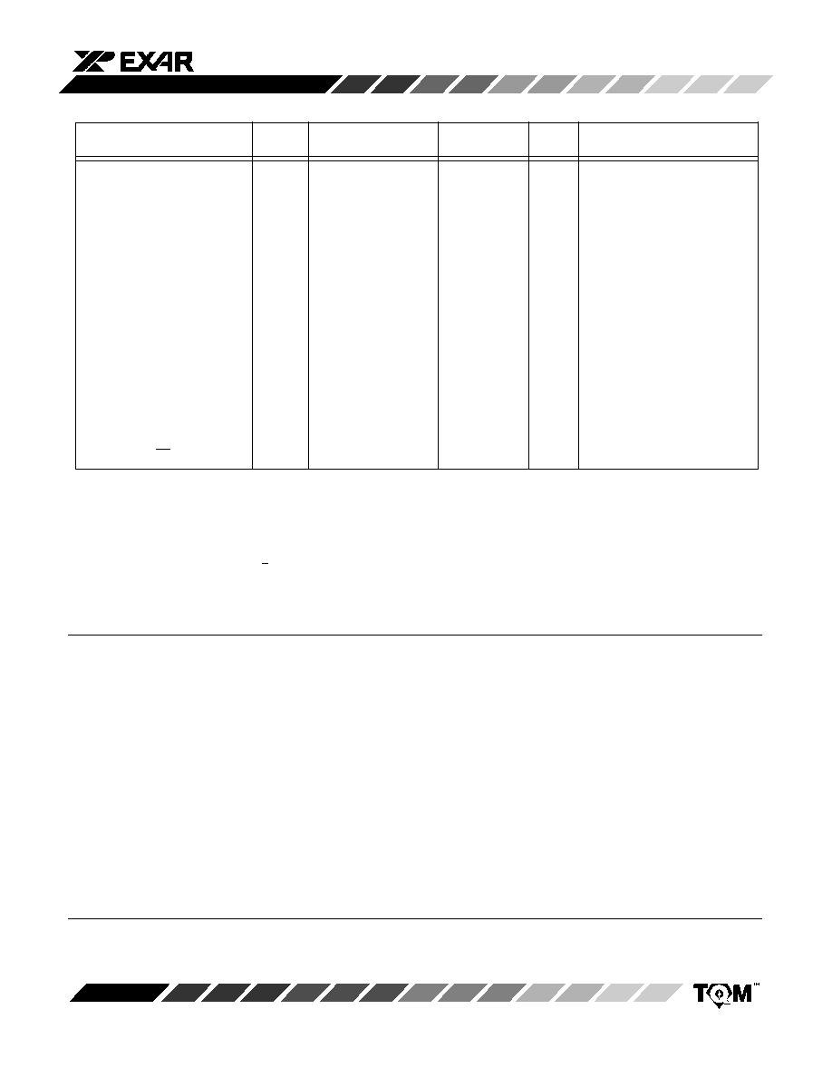
PIN CONFIGURATIONS
See Packaging Section for
Package Dimensions
13
16
14
15
1
2
3
4
5
6
7
8
9
10
28
27
26
25
24
23
22
21
20
19
11
18
12
17
28 Pin PDIP (0.300")
NN28
VR1
VO1
VO2
VR2
GND
VO4
VR4
VR5
VO5
VO6
VR0
VO0
CS3P
CS2P
SDI
CS1P
SDO
CLK
CSOP
VO7
VR7
VR6
V
CC
VR3
VO3
V
EE
28
1
15
14
2
3
4
5
6
7
17
16
8
9
19
18
10
11
23
22
21
20
27
26
25
24
12
13
VR0
28 Pin SOIC (EIAJ, 0.335")
R28
VO0
CS3P
CS2P
SDI
CS1P
SDO
CLK
CSOP
VO7
VR7
VR6
VR1
VO1
VO2
VR2
GND
VO4
VR4
VR5
VO5
VO6
VR3
VO3
V
CC
V
EE
RST
LD
RST
LD
PIN OUT DEFINITIONS
1
VR1
DAC 1 Reference Input
2
VO1
DAC 1 Output
3
VO2
DAC 2 Output
4
VR2
DAC 2 Reference Input
5
VR3
DAC 3 Reference Input
6
VO3
DAC 3 Output
7
V
CC
Positive Supply
8
V
EE
Negative Supply
9
GND
Ground
10
VO4
DAC 4 Output
11
VR4
DAC 4 Reference Input
12
VR5
DAC 5 Reference Input
13
VO5
DAC 5 Output
14
VO6
DAC 6 Output
15
VR6
DAC 6 Reference Input
PIN NO.
NAME
DESCRIPTION
16
VR7
DAC 7 Reference Input
17
VO7
DAC 7 Output
18
CSOP
Chip Select Bit 0 (LSB)
19
CS1P
Chip Select Bit 1
20
SDI
Serial Data/Address Input
21
SDO
Serial Data Output
22
CLK
Shift Register Clock
23
LD
Load Signal; Load Data
to Selected DACs
24
RST
Reset Signal; Reset all DACs to
V
REF
/2
25
CS2P
Chip Select Bit 2
26
CS3P
Chip Select Bit 3 (MSB)
27
VO0
DAC 0 Output
28
VR0
DAC 0 Reference Input
PIN NO.
NAME
DESCRIPTION
MP7651
4
Rev. 2.00
ELECTRICAL CHARACTERISTICS TABLE
Unless Otherwise Noted: V
CC
= +5 V, V
EE
= 5 V and 3 V, V
REF
= 3 V and 3 V, T = 25
°
C,
Output Load = Open
25
°
C
Tmin to Tmax
Parameter
Symbol
Min
Typ
Max
Min
Max
Units
Test Conditions/Comments
DC CHARACTERISTICS
Resolution (All Grades)
N
8
8
Bits
Differential Non-Linearity
DNL
+0.8
+1
LSB
Integral Non-Linearity
INL
+1
+1
LSB
Monotonicity
Guaranteed
Guaranteed
Gain Error
GE
+1.5
+1.5
% FSR
FSR = Full Scale Range (1)
Zero Scale Offset
Z
OFS
+20
+75
+75
mV
Output Drive Capability
I
O
+1
mA
REFERENCE INPUTS
Impedance of V
REF
REF
6
12
18
6
18
k
Voltage Range
V
R
V
EE
+1.5
V
CC
1.8
V
V
REF
Max Swing is AGND +3 V
DYNAMIC
CHARACTERISTICS
2
R
L
= 5 k, C
L
= 20 pF
Input to Output Bandwidth
10
MHz
V
R
= 1.6 V pp, R
L
= 5k to V
EE
Input to Output Settling Time
5
150
ns
V
R
= 1.6 V pp, R
L
= 5k to V
EE
Small Signal Voltage Reference
t
r
10
MHz
V
OUT
=50mV p-p above code 16
Input to Output Bandwidth
Small Signal Voltage Reference
t
r
5
8
MHz
V
OUT
=50mV p-p for all codes
Input to Output Bandwidth
Voltage Settling from V
REF
to
t
sr
275
300
325
ns
V
R
=0 to V
R
= 3V Step (6)
V
DAC
Out
to 1 LSB
Voltage Settling from Digital
t
sd
275
300
325
ns
ZS to FS to 1 LSB
Code to V
DAC
Out
V
REF
Feedthrough
F
DT
65
dB
Codes=0 @ 1 MHz
Group Delay
GD
20
ns
Harmonic Distortion
T
HD
0.5
%
V
REF
=1MHz Sine 3V p-p
Channel-to-Channel Crosstalk
C
T
75
dB
@ 1 MHz, single channel
Digital Feedthrough
Q
1
nVs
CLK to V
OUT
Power Supply
PSRR
0.02
%/%
V = +5%
Rejection Ratio
POWER CONSUMPTION
Positive Supply Current
I
CC
15
25
30
mA
V
REF
= 0 V
Negative Supply Current
I
EE
15
25
30
mA
V
REF
= 0 V
Power Dissipation
P
DISS
150
250
300
mW
V
REF
= 0 V, Codes = all 1
DIGITAL INPUT
CHACTERISTICS
Logic High
3
V
IH
2.4
2.4
V
Logic Low
3
V
IL
0.8
0.8
V
Input Current
I
L
+10
+10
µ
A
Input Capacitance
2
C
L
8
8
pF
MP7651
5
Rev. 2.00
ELECTRICAL CHARACTERISTICS TABLE
Description
Symbol
Min
Typ
Max
Min
Max
Units
Conditions
DIGITAL TIMING
SPECIFICATIONS
2, 4
Input Clock Pulse Width
t
CH
, t
CL
40
50
ns
Data Setup Time
t
DS
10
10
ns
Data Hold Time
t
DH
15
15
ns
CLK to SDO Propagation Delay
t
PD
40
50
ns
DAC Register Load Pulse Width
t
LD
100
100
ns
Reset Pulse Width
t
RST
50
60
ns
Clock Edge to Load Rising Edge
t
CKLD1
100
100
ns
Clock Edge to Load Falling Edge
t
CKLD2
0
0
ns
Load Falling Edge to SDO
t
HZ1
50
60
ns
3-state Enable
Load Rising Edge to SDO
t
HZ2
35
50
ns
3-state Disable
Load Falling Edge to CLK Disable
t
LDCK1
25
40
ns
Load Rising Edge to CLK Enable
t
LDCK2
35
50
ns
LD Set-up Time with Respect
t
LDSU
15
20
ns
to CLK
CS0-CS3 Set-Up Time with
t
CSLD
25
35
ns
Respect to LD
25
°
C
Tmin to Tmax
NOTES:
1
Full Scale Range (FSR) is 3V.
2
Guaranteed but not production tested.
3
Digital Input levels should not go below ground or exceed the positive supply voltage, otherwise damage may occur.
4
See Figures 2 and 3.
5
For reference input pulse: t
R
= t
F
> 100 ns.
Specifications are subject to change without notice
ABSOLUTE MAXIMUM RATINGS (TA = +25
°
C unless otherwise noted)
1, 2
V
CC
to GND
+6.5 V
. . . . . . . . . . . . . . . . . . . . . . . . . . . . . . . . . .
V
EE
to GND
6.5 V
. . . . . . . . . . . . . . . . . . . . . . . . . . . . . . . . . .
V
Ri
to GND
V
CC
to V
EE
. . . . . . . . . . . . . . . . . . . . . . . . . . . . . . .
V
Oi
to GND
V
CC
to V
EE
. . . . . . . . . . . . . . . . . . . . . . . . . . . . . . .
Digital Input & Output Voltage
to GND
GND 0.5 to V
CC
+0.5 V
. . . . . . . . . . . . . . . . . . . .
Operating Temperature Range
Extended Industrial
40
°
C to +85
°
C
. . . . . . . . . . . . . . . . . . .
Maximum Junction Temperature
150
°
C
. . . . . . . . . . . . . . . . .
Storage Temperature
65
°
C to +150
°
C
. . . . . . . . . . . . . . . . .
Lead Temperature (Soldering, 10 sec)
+300
°
C
. . . . . . . . . . .
Package Power Dissipation Rating @ 75
°
C
PDIP, SOIC
1000mW
. . . . . . . . . . . . . . . . . . . . . . . . . . . . .
Derates above 75
°
C
6mW/
°
C
. . . . . . . . . . . . . . . . . . . . . .
NOTES:
1
Stresses above those listed under "Absolute Maximum Ratings" may cause permanent damage to the device. This is a
stress rating only and functional operation at or above this specification is not implied. Exposure to maximum rating
conditions for extended periods may affect device reliability.
2
Any input pin which can see a value outside the absolute maximum ratings
should be protected by Schottky diode clamps
(HP5082-2835) from input pin to the supplies.
All inputs have protection diodes which will protect the device from short
transients outside the supplies of less than 100mA for less than 100
µ
s.
APPLICATIONS INFORMATION
Refer to Section 8 for Applications Information