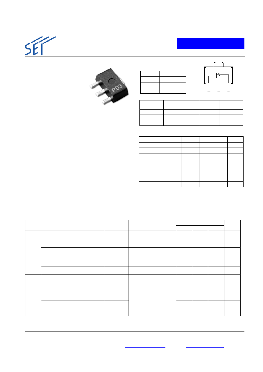
Technical Note
P0120003P
800mW GaAs Power FET (Pb-Free Type)
SUMITOMO ELECTRIC
Specifications and information are subject to change without notice. 2003-11
Sumitomo Electric Industries, Ltd. 1,Taya-cho, Sakae-ku, Yokohama, 244-8588 Japan
Phone: +81-45-853-7263 Fax: +81-45-853-1291 e-mail :
GaAsIC-ml@ml.sei.co.jp
Features
4
1
2
3
4
1
2
3
· Up to 2.7 GHz frequency band
Web Site:
www.sei.co.jp/GaAsIC/
· Beyond +27 dBm output power
· Up to +43dBm Output IP3
· High Drain Efficiency
· 12dB Gain at 2.1GHz
· SOT-89 SMT Package
· Low Noise Figure
Applications
·Wireless communication system
·Cellular, PCS, PHS, W-CDMA, WLAN
Description
P0120003P is a high performance GaAs MESFET housed in
a low-cost SOT-89 package. Our originally developed
"pulse-doped" channel structure has realized low distortion,
which leads to high IP3. The channel structure also achieved
an extremely low noise figure. The details about pulse-doped
FET channel are described in our products catalog.
Utilization of AuSn die attach has realized a low and stable
thermal resistance. The lead frame is plated with Sn-Bi to
make the device Pb-free.
SEI's long history of manufacturing has cultivated high
device reliability. The estimated MTTF of the FET is longer
than 15years at Tj of 150°C. You can see the details in
Reliability and Quality Assurance.
Functional Diagram
Pin No.
Function
1 Input/Gate
2, 4
Ground
3 Output/Drain
Ordering Information
Part No
Description
Number
of devices
Container
P0120003P
GaAs Power FET
1000
7" Reel
KP023J
2.11-2.17GHz
Application Circuit
1
Anti-static
Bag
Absolute Maximum Ratings
(@Tc=25°C)
Parameter Symbol
Value
Units
Drain-Source Voltage
Vds
8
V
Gate-Source Voltage
Vgs
- 4
V
Drain Current
Ids
Idss
---
RF Input Power
(continuous)
Pin 20
(*)
dBm
Power Dissipation
Pt 2.2 W
Junction Temperature
Tj
125
°C
Storage Temperature
Tstg
- 40 to +125
°C
Tc: Case Temperature. Operating the device beyond any of these
values may cause permanent damage.
(*) Measured at 2.1GHz with our test fixture matched to OIP3.
Electrical Specifications (@Tc=25°C)
Values
Parameter Symbol
Test
Conditions
Min. Typ. Max.
Units
Saturated Drain Current
Idss
Vds=3V, Vg=0V
---
---
850
mA
Transconductance gm
Vds=6V, Ids=300mA
250
---
---
mS
Pinchoff Voltage
Vp
Vds=6V, Ids=30mA
- 3.0
---
- 1.7
V
Gate-Source Breakdown Voltage
|Vgs0|
Igso= - 30
µA
3.0 --- --- V
DC
Thermal Resistance
Rth
Channel-Case
---
--- 45
°C/W
Frequency f
2.7
GHz
Output Power
@ 1dB Gain Compression
P1dB
29
---
dBm
Small Signal Gain
G
12
---
dB
Output IP3
OIP3
---
43
---
dBm
RF
Power Added Efficiency
add
Vds=6V
Ids=220mA
f=2.1GHz
---
56 --- %
-1-
Technical Note
P0120003P
800mW GaAs Power FET (Pb-Free Type)
SUMITOMO ELECTRIC
Typical Characteristics
T
o
t
a
l P
o
w
e
r D
i
s
s
ip
a
t
i
o
n
(
W
)
Tc (°C)
3
4
2
1
0
0
50
100
150
200
Vgs=0V
-2.0V
-1.5V
-1.0V
-0.5V
D
r
a
i
n C
u
r
r
e
nt
(
m
A
)
Vds (V)
1000
50
100
150
200
Vgs=0V
-2.0V
-1.5V
-1.0V
-0.5V
D
r
a
i
n C
u
r
r
e
nt
(
m
A
)
Vds (V)
1000
750
500
250
0
750
500
250
0
0
2
4
6
8
Transfer Curve
Power Derating Curve
Load-pull Characteristics (Typical Data)
Tc=25°C, Vds=6V, Ids=220mA, Common Source, Zo=50
(Calibrated to device leads)
0
45
90
135
-180
-135
-9
0
-45
0
45
90
135
-180
-135
-9
0
-45
S12
S21
1.2GHz
1.2GHz
2.4GHz
2.4GHz
2.0
6.0
4.0
0
0.02
0.04
0.06
0
Scale for |S12|
Sc
a
l
e
fo
r |
S
2
1
|
0
1.
0
1.
0
-1
.
0
10
.
0
10.0
-10
.0
5.
0
5.0
-5.
0
2.
0
2.
0
-2
.0
3.
0
3.0
-3.
0
4.
0
4.0
-4.
0
0.
2
0.2
-0.2
0.
4
0.4
-0.
4
0.
6
0.
6
-0
.6
0.
8
0.
8
-0
.8
0
1.
0
1.
0
-1
.
0
10
.
0
10.0
-10
.0
5.
0
5.0
-5.
0
2.
0
2.
0
-2
.0
3.
0
3.0
-3.
0
4.
0
4.0
-4.
0
0.
2
0.2
-0.2
0.
4
0.4
-0.
4
0.
6
0.
6
-0
.6
0.
8
0.
8
-0
.8
S11
S22
1.2GHz
1.2GHz
2.4GHz
2.4GHz
Specifications and information are subject to change without notice. 2003-11
Sumitomo Electric Industries, Ltd. 1,Taya-cho, Sakae-ku, Yokohama, 244-8588 Japan
Phone: +81-45-853-7263 Fax: +81-45-853-1291 e-mail :
GaAsIC-ml@ml.sei.co.jp
-2-
Web Site:
www.sei.co.jp/GaAsIC/
Technical Note
P0120003P
800mW GaAs Power FET (Pb-Free Type)
SUMITOMO ELECTRIC
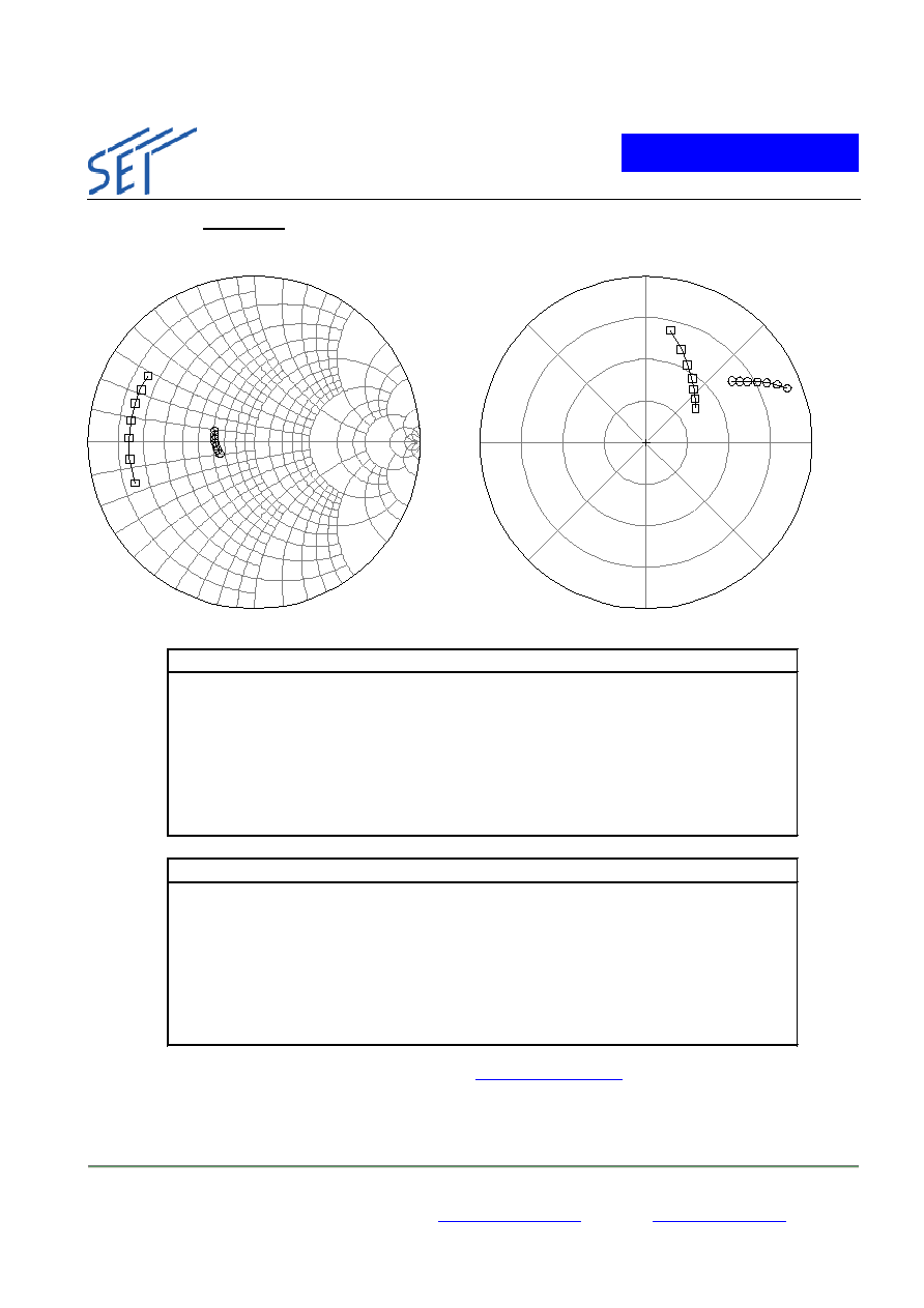
Tc=25°C, Vds=6V, Ids=180mA, Common Source, Zo=50
(Calibrated to device leads)
Specifications and information are subject to change without notice. 2003-11
Sumitomo Electric Industries, Ltd. 1,Taya-cho, Sakae-ku, Yokohama, 244-8588 Japan
Phone: +81-45-853-7263 Fax: +81-45-853-1291 e-mail :
GaAsIC-ml@ml.sei.co.jp
Web Site:
www.sei.co.jp/GaAsIC/
0
0
1.
0
1.
0
-1
.0
10
.
0
10.0
-10
.0
5.
0
5.0
-5.
0
2.0
2.
0
-2
.0
3.
0
3.0
-3.
0
4.0
4.0
-4.
0
0.2
0.2
-0.2
0.4
0.4
-0
.4
0.
6
0.
6
-0
.6
0.
8
0.
8
-0
.8
1.
0
1.
0
-1
.0
10
.
0
10.0
-10
.0
5.
0
5.0
-5.
0
2.0
2.
0
-2
.0
3.
0
3.0
-3.
0
4.0
4.0
-4.
0
0.2
0.2
-0.2
0.4
0.4
-0
.4
0.
6
0.
6
-0
.6
0.
8
0.
8
-0
.8
S11
S22
1.2GHz
1.2GHz
2.4GHz
2.4GHz
0
45
90
13
5
-180
-135
-9
0
-4
5
0
45
90
13
5
-180
-135
-9
0
-4
5
S12
S21
1.2GHz
1.2GHz
2.4GHz
2.4GHz
2.0
6.0
4.0
0
0.02
0.04
0.06
0
Scale for |S12|
S
c
al
e f
o
r
|
S
2
1
|
Ids
Ids
=220mA Freq (GHz) S11 Mag
S11 Ang
S21 Mag
S21 Ang
S12 Mag
S12 Ang
S22 Mag
S22 Ang
1.2
0.760
-161.1
5.548
77.6
0.049
36.8
0.204
-160.1
1.4
0.756
-172.5
4.827
69.3
0.052
34.4
0.212
-166.9
1.6
0.754
178.0
4.263
61.7
0.056
32.3
0.219
-172.7
1.8
0.754
169.6
3.812
54.6
0.060
30.0
0.225
-178.1
2.0
0.755
162.0
3.454
47.9
0.063
27.7
0.229
176.5
2.2
0.755
154.9
3.163
41.3
0.067
25.2
0.233
171.2
2.4
0.754
148.0
2.925
34.8
0.072
22.4
0.238
164.9
=180mA Freq (GHz) S11 Mag
S11 Ang
S21 Mag
S21 Ang
S12 Mag
S12 Ang
S22 Mag
S22 Ang
1.2
0.758
-161.1
5.539
77.7
0.051
35.5
0.215
-161.3
1.4
0.754
-172.5
4.820
69.3
0.054
33.1
0.223
-168.2
1.6
0.753
178.0
4.256
61.8
0.057
30.9
0.229
-174.0
1.8
0.753
169.6
3.805
54.7
0.061
28.6
0.235
-179.5
2.0
0.753
162.0
3.449
48.0
0.065
26.3
0.239
175.0
2.2
0.753
154.9
3.158
41.4
0.069
23.8
0.243
169.6
2.4
0.752
148.0
2.920
34.9
0.073
21.0
0.248
163.4
[Note]
You can download the S-parameter list from our web site:
www.sei.co.jp/GaAsIC
/
-3-
Technical Note
P0120003P
800mW GaAs Power FET (Pb-Free Type)
SUMITOMO ELECTRIC
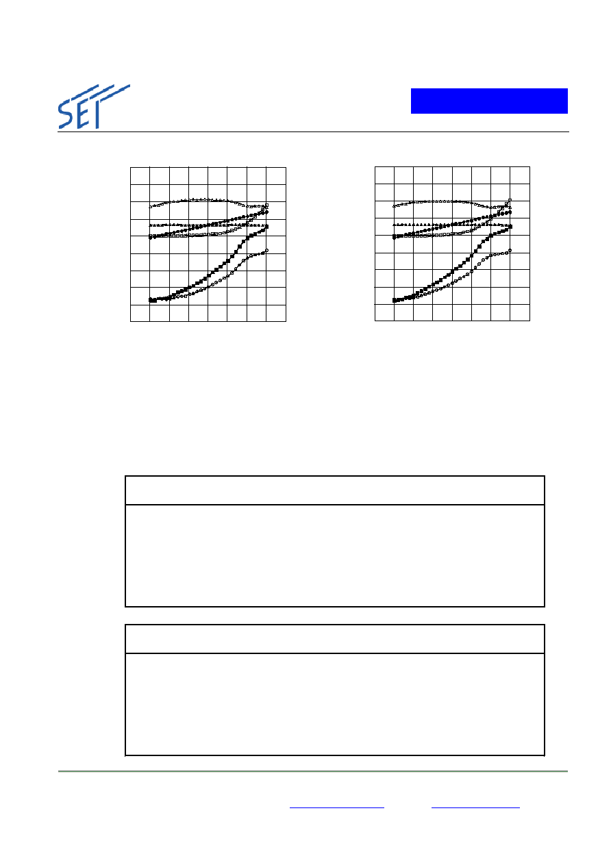
Ids=220mA Ids=180mA
-100
-80
-60
-40
-20
0
20
40
60
80
Po
u
t
(
d
B
m
)
IM
3
(
d
B
m
)
IP
3
(
d
B
m
)
IM
3
/
P
o
u
t
(
d
B
c
)
ad
d
(
%
)
-20
-15
-10
-5
0
5
10
15
20
Pin (dBm)
Pout
Gain
IP3
add
IM3
IM3/Pout
-100
-80
-60
-40
-20
0
20
40
60
80
Po
u
t
(
d
B
m
)
IM
3
(
d
B
m
)
IP
3
(
d
B
m
)
IM
3
/
P
o
u
t
(
d
B
c
)
ad
d
(
%
)
-20
-15
-10
-5
0
5
10
15
20
Pin (dBm)
Pout
Gain
IP3
add
IM3
IM3/Pout
-20
-15
-10
-5
0
5
10
15
20
Pin (dBm)
Pout
Gain
IP3
add
IM3
IM3/Pout
-20
-100
-80
-60
-40
-20
0
20
40
60
80
-15
-10
-5
0
5
10
15
20
Po
u
t
(
d
B
m
)
IM3
(
d
B
m
)
IP
3
(
d
B
m
)
IM
3
/
P
o
u
t
(
d
B
c
)
ad
d
(
%
)
Pin (dBm)
Pout
Gain
IP3
add
IM3
IM3/Pout
-100
-80
-60
-40
-20
0
20
40
60
80
-15
-10
-5
0
5
10
15
20
Po
u
t
(
d
B
m
)
IM3
(
d
B
m
)
IP
3
(
d
B
m
)
IM
3
/
P
o
u
t
(
d
B
c
)
ad
d
(
%
)
Pin (dBm)
Pout
Gain
IP3
add
IM3
IM3/Pout
Device: P0120003P
Frequency: f1=2.1GHz, f2=2.101GHz
Bias: Vds=6V, Ids=220mA
Source Matching: Mag 0.61 Ang -159.3°
Load Matching: Mag 0.48 Ang -155.4°
Device:P0120003P
Frequency: f1=2.1GHz, f2=2.101GHz
Bias:Vds=6V,Ids=180mA
Source Matching:Mag 0.61 Ang -159.3°
Load Matching: Mag 0.437 Ang -160.7°
[Note] P
out
and
add
are measured by one signal.
The data for the figures above were measured with the load impedance matched to IP3.
Id=220mA
Pin
(dBm)
Pout
(dBm)
Gain
(dB)
IM3
(dBm)
IM3/Pout
(dBc)
IP3
(dBm)
Id
(mA)
add
(%)
-15.0
-2.0
13.0
-75.0
-73.0
34.5
220.5
0.0
-10.0
3.2
13.2
-70.2
-73.3
39.9
219.1
0.2
-5.0
8.1
13.1
-59.5
-67.7
42.1
216.4
0.5
0.0
13.1
13.1
-46.0
-59.0
42.6
212.0
1.5
5.0
18.0
13.0
-28.5
-46.5
41.0
205.3
4.9
10.0
23.1
13.1
-2.5
-25.7
35.2
207.5
15.7
15.0
27.6
12.6
11.1
-16.5
33.8
252.6
35.8
Id=180mA
Pin
(dBm)
Pout
(dBm)
Gain
(dB)
IM3
(dBm)
IM3/Pout
(dBc)
IP3
(dBm)
Id
(mA)
add
(%)
-15.0
-1.7
13.3
-75.4
-73.7
35.1
178.2
0.1
-10.0
3.5
13.5
-68.7
-72.2
39.6
177.1
0.2
-5.0
8.4
13.4
-56.1
-64.5
40.7
174.8
0.6
0.0
13.4
13.4
-41.3
-54.7
40.7
171.2
2.0
5.0
18.4
13.4
-23.0
-41.3
39.0
165.1
6.6
10.0
23.4
13.4
0.6
-22.8
33.9
173.1
20.1
15.0
27.6
12.6
11.1
-16.5
34.0
216.4
41.9
Specifications and information are subject to change without notice. 2003-11
Sumitomo Electric Industries, Ltd. 1,Taya-cho, Sakae-ku, Yokohama, 244-8588 Japan
Phone: +81-45-853-7263 Fax: +81-45-853-1291 e-mail :
GaAsIC-ml@ml.sei.co.jp
-4-
Web Site:
www.sei.co.jp/GaAsIC/
Specifications and information are subject to change without notice. 2003-11
Sumitomo Electric Industries, Ltd. 1,Taya-cho, Sakae-ku, Yokohama, 244-8588 Japan
Phone: +81-45-853-7263 Fax: +81-45-853-1291 e-mail :
GaAsIC-ml@ml.sei.co.jp
Web Site:
www.sei.co.jp/GaAsIC/
-5-
Technical Note
P0120003P
800mW GaAs Power FET (Pb-Free Type)
SUMITOMO ELECTRIC
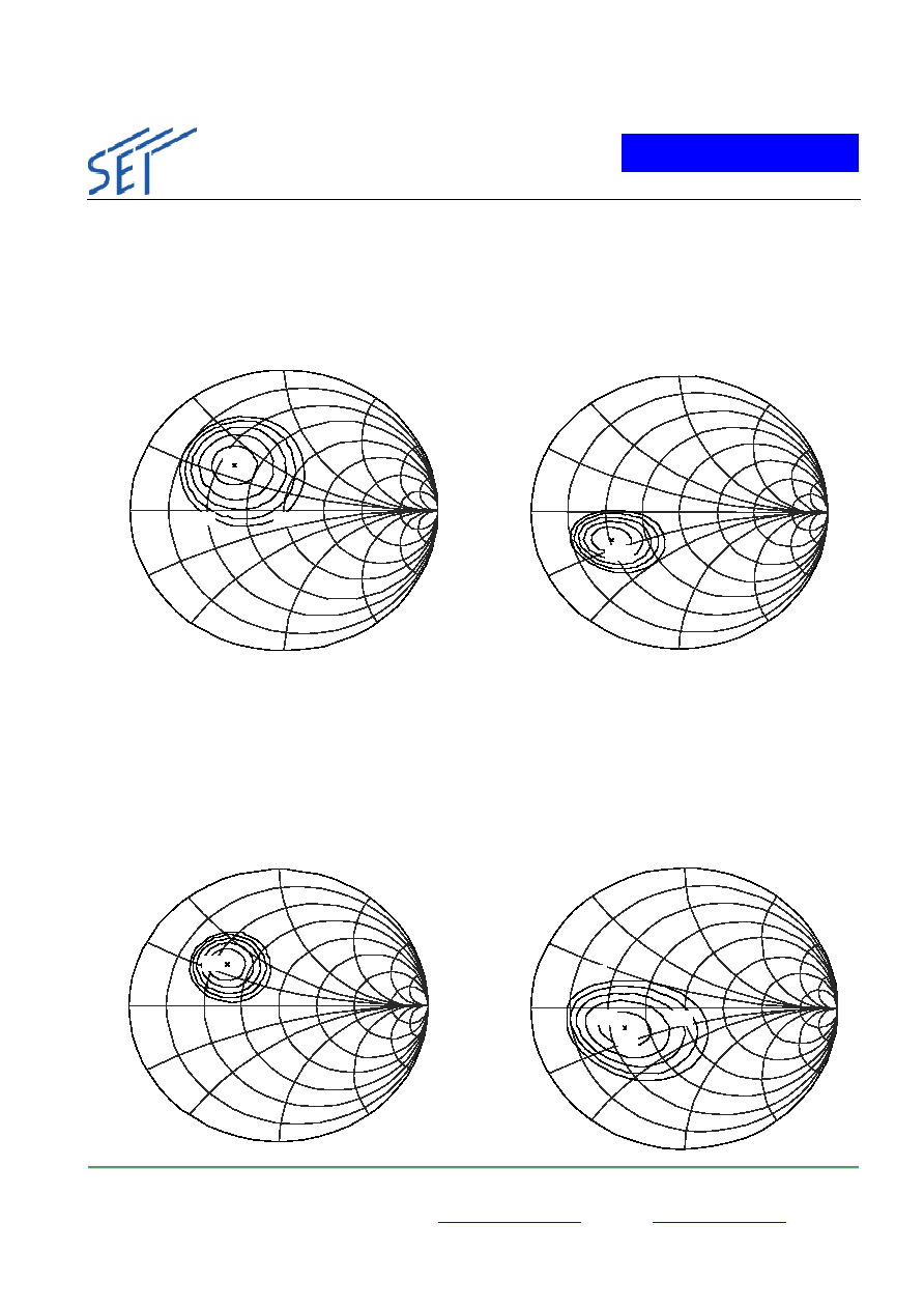
Tc=25°C, Vds=6V, Ids=220mA, Pin=0d Bm
[Pout-Lstate]
f = 2.1GHz
pout
: 0.46
135.5
Source : 0.76
-166.1
Pout max : 14.4d Bm
[IP3-Lstate]
f1 = 2.1GHz
f2 = 2.101GHz
IP3
: 0.52
-155.9
Source : 0.73
-170.1
IP3 max : 40.45d Bm
Tc=25°C, Vds=6V, Ids=180mA, Pin=0d Bm
[Pout-Lstate]
f = 2.1GHz
pout
: 0.46
138.7
Source : 0.76
-166.1
Pout max : 14.4d Bm
[IP3-Lstate]
f1 = 2.1GHz
f2 = 2.101GHz
IP3
: 0.42
-160.2
Source : 0.73
-170.1
IP3 max : 39.3d Bm
+j50
13.15
14.4
+j25
+j100
-j100
-j50
-j25
25
50
100
+j50
13.15
14.4
+j25
+j100
-j100
-j50
-j25
25
50
100
39.2
+j25
+j50
+j100
-j100
-j50
-j25
25
50
100
40.45
39.2
+j25
+j50
+j100
-j100
-j50
-j25
25
50
100
40.45
+j50
36.8
+j25
+j100
-j100
-j50
-j25
25
50
100
39.3
36.8
+j25
+j100
-j100
-j50
-j25
25
50
100
39.3
13.9
+j25
+j50
+j100
-j100
-j50
-j25
25
50
100
14.4
13.9
+j25
+j50
+j100
-j100
-j50
-j25
25
50
100
14.4