1
Edition 1.1
July 2004
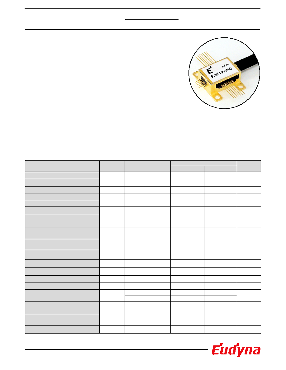
Driver Integrated 10Gb/s
MI-DFB LD Module
FTM1141GF-C
Parameter
Condition
Symbol
Operating Case Temperature
Top(Tc)
°C
Modulator (Mod) Modulation
Control Voltage
Vm
V
Mod Bias Control Voltage
Vb
V
Power Supply Voltage
Vss
V
Laser Forward Current
If
mA
CW
Laser Reverse Voltage
VR
V
CW
Storage Temperature
Tstg
°C
Differential
(AC-coupled)
Data Input Voltage
Din, DinB
Vpp
Note (1-1)
ESD Tolerance
Vesd
V
Note (1-2)
ESD Tolerance
Vesd
V
Photodiode Forward Current
-
-
mA
Photodiode Reverse Voltage
VDR
V
260
°C MAX
Lead Soldering Time
sec
Cooling
Heating
TEC Voltage
Vc
V
Cooling
Heating
A
TEC Current
Ic
Tth
Thermistor Temperature
°C
CW
Optical Output Power
Pf
mW
Unit
ABSOLUTE MAXIMUM RATINGS (Top=25
°C, Unless otherwise specified)
Limits
0
-6.5
-6.5
-6.5
-
-
-40
-
-
-
-
-
-
ATC operation
-
-1.0
-
-0.5
0
-
Min.
Vss-4.8
(min-6.5)
Cross Point Control Voltage
Vx1,(Vx2)
V
75
Vss+1.2
(max0)
Vss+2.4
(max0)
0
150
2
85
1.6
50
200
1
10
10
2.5
-
1.5
-
+75
5
Max.
Vss+2.4
(max0)
FEATURES
· Driver integrated 10Gb/s MI-DFB module for 1600ps/nm
optical transmission
· MI-DFB-LD (Modulator Integrated DFB Laser Diode) is installed
· Modulator driver IC is installed
· Built-in optical isolator, PIN-Photo diode for monitor, thermistor
and thermo-electric cooler
· 1600ps/nm (80km)
DESCRIPTION
The FTM1141GF-C was developed to reduce the size and technical
complexity of 10Gb/s optical board designs. This product, which includes
a driver and modulator integrated laser in one package, eliminates the
customer concerns regarding how to handle the RF interfacing between
these two components on his board. By co-packaging these components
a solution has also been achieved that offers greatly reduced board space.
This reduction in space is critical for next generation transponder applications.
The FTM1141GF-C has been designed with a differential co-planar electrical interface
which allows for easy interfacing to RF lines on PC boards. The package and pinout are part of a
multi-source agreement. This product is designed for 80km SONET/SDH applications and single
channel drop links in DWDM systems.
Parameter
Limit
LASER DIODE AND MODULATOR CHARACTERSITICS
OPTICAL SPECIFICATIONS (TLD=25°C, Top=0 to 75°C and BOL, unless otherwise specified)
Unit
Symbol
Condition
Min.
Max.
Typ.
Optical Output Power
dBm
Pop
+1.0
+3.5
-
Note (2a)
Forward Voltage
V
VF
-
2.2
1.4
CW, IF=Iop
Extinction Ratio
dB
Rext
9.0
-
-
Pf=Pop, Note (2a)
Peak Wavelength
nm
Wp
1530
1565
-
Pf=Pop, Note (2a)
Side Mode Suppresion
Ratio
dB
SSR
35
-
-
IF=Pop, CW
Optical Rise Time
psec
Tr
-
30
-
Note (3), 20% to 80%
Optical Fall Time
psec
Tf
-
30
-
Note (3), 20% to 80%
Optical Isolation
dB
Is
25
-
-
Tracking Error
dB
TE
-0.5
+0.5
-
Note (2a)
Input Return Loss
dB
S11
6
-
-
130KHz to 10GHz
Dispersion Penalty
dB
dP
-
2.0
-
Note (2)
Eye Pattern Mask
Msk
Error Free
Note (2a), 500 counts
CW
Threshold Current
Ith
mA
-
-
25
-
mA
Pf=Pop
Operating Current
Iop
40
100
70
Parameter
Limit
MONITOR DIODE CHARACTERISTICS
Unit
Symbol
Condition
Min.
Max.
Typ.
Monitor Diode Capacitance
pF
Ct
-
15
5
VDR=5V, f=1MHz
IF=Iop, VDR=5V
Monitor Current
Im
µA
100
1500
-
nA
VDR=5V
Monitor Dark Current
Id
-
100
2
Parameter
Limit
TEC & THERMISTOR CHARACTERISTICS
Unit
Symbol
Condition
Min.
Max.
Typ.
TEC Power Consumption
W
K
Pc
-
2.0
-
Note (4)
Thermistor Resistance
k
Rth
-
-
10
TLD=25
°C
25/75
°C
Thermistor B Constant
B
3270
3630
3450
Note (4)
TEC Current
Ic
A
-
1.0
-
V
Note (4)
TEC Voltage
Vc
-
2.0
-
2
Driver Integrated 10Gb/s
MI-DFB LD Module
FTM1141GF-C
3
Driver Integrated 10Gb/s
MI-DFB LD Module
FTM1141GF-C
Parameter
Limit
DRIVER IC CHARACTERISTICS
Unit
Symbol
Condition
V
Vpp
Min.
Max.
Typ.
Modulator (Mod) Modulation
Control Voltage
V
Vm
Vss
Vss
+1.0
-
Mod Bias Control Voltage
V
Vb
Vss
Vss
+2.2
-
Differential (AC Coupled)
Data Input Voltage
Din, DinB
0.5
1.0
-
Xp=50%
Cross Point (XP) Control
Voltage
Vx1, (Vx2)
Vss
+0.8
Vss
+2.2
-
Driver IC Supply Voltage
Vss
V
-5.5
-4.9
-5.2
mA
Driver IC Supply Current
Iss
-
285
-
Note (1-1): Pin No. 3,4,5,6,7,9,11 (Human Body Model)
Note (1-2): Pin No. 1,2,8,10,12-19 (Human Body Model)
Note (2): Eudyna Test System
(a) Drive Condition
Bit Rate:
9.95328 Gb/s
Word Pattern:
PRBS=2
31
-1
Mark Density:
50%
Laser Bias Current:
Iop
Laser Temperature(TLD):
25
°C
Eye Pattern Mask:
ITU-T Eye mask for STM-64
(b) Fiber Dispersion
1600ps/nm
(c) Dispersion Penalty
Bit Error Rate=10
-12
Note (3): Eudyna Test System
Vb, Vm, Vx1(Vx2) is set to make Pop and Rext within the specification
Note (4): Eudyna Test System
Operating Case Temperature: Top=+75°C
Laser Temperature:
25
°C
Optical Output Power:
Pf=Pop, Note (2a)
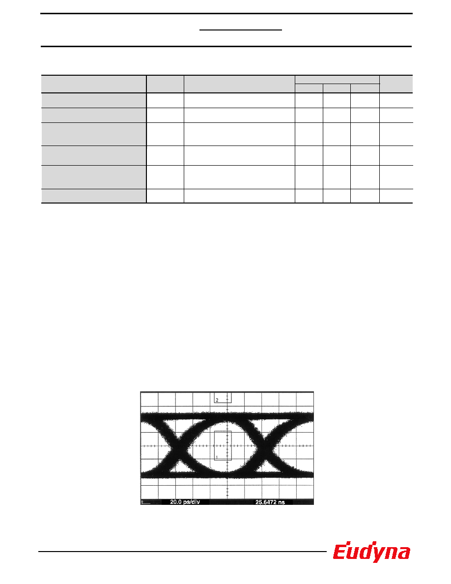
Typical Output Waveform
Back to Back (with Filter)
9.95328Gb/s, NRZ, PRBS=2
31
-1, TLD=TC=25°C

4
Driver Integrated 10Gb/s
MI-DFB LD Module
FTM1141GF-C
PD
PD
LD
NC
NC
TEC
GND
GND
Blocking
Capacitor
Ex. 0.1µF
Din
GND
DinB
GND
Vx1
Vx2
Cross Point Control
Bias Voltage Control
Supply Voltage
Modulation Voltage Control
VSS
Vm
Vb
Ther r
TEC
Chip
Capacitor
0.1µF
Chip
Capacitor
0.1µF
Typical Application for Driver IC
For stable operation:
8-1. To prevent a dependence of "Cross point" on the supply voltage VSS,
(1) Use an external voltage source of -3.8V for "Vx2", or
(2) Control the voltage of "Vx1", so that the voltage difference "Vx1-Vx2" remain constant.
8-2. To prevent a dependence of "Modulation control voltage" on the supply voltage VSS,
control the voltage of "Vm", so that the difference "Vm-VSS" remain constant.
8-3. To prevent a dependence of "Bias control voltage" on the supply voltage VSS,
control the voltage of "Vb", so that the difference "Vb-VSS" remain constant.

5
14-0.3
6.00
±0.25
5-0.15
±
0.08
4.95
22.0
18.0
12.0
35
±
1
Ř0.9
±
0.1
Ř5.20
±
0.25
4-Ř2.6
±0.2
NOTE: Pigtail length (L)
shall be specified in the
detail (individual) specification.
CONNECTOR
DETAIL-B
L
5.3
17.6
Detail A
Detail B
13.6
9.6
19
13
1
7
8
12
25.0
±0.5
1.25
(3)
0.5
7.7
14-0.2
4.86
±0.20
1.25
4.56
4.46
±
0.20
3.56
5-0.3
4-P1.0
4.00
±
0.25
Pin Description
1. Thermoelectric cooler(Anode, +)
2. Thermistor
3. Vb: Modulator bias control voltage
4. Vm: Modulator modulation voltage control voltage
5. Vss: Driver IC supply voltage
6. Vx2: Cross point control voltage
7. Vx1: Cross point control voltage
8. Case Ground
9. DinB: Inverted data input voltage
10. Case Ground
11. Din: Data Input voltage
12. Case Ground
13. Monitor photo diode(Cathode)
14. Monitor photo diode(Anode)
15. Case Ground
16. LD Bias(Anode)
17. NC
18. NC
19. Thermoelectric cooler(Cathode, -)
12-P1.0
5.8
DETAIL-A
"GF" PACKAGE
UNIT: mm
Driver Integrated 10Gb/s
MI-DFB LD Module
FTM1141GF-C
Eudyna Devices Inc. products contain gallium arsenide
(GaAs) which can be hazardous to the human body and the environment.
For safety, observe the following procedures:
CAUTION
· Do not put this product into the mouth.
· Do not alter the form of this product into a gas, powder, or liquid
through burning, crushing, or chemical processing as these by-products
are dangerous to the human body if inhaled, ingested, or swallowed.
· Observe government laws and company regulations when discarding this
product. This product must be discarded in accordance with methods
specified by applicable hazardous waste procedures.
For further information please contact:
Eudyna Devices USA Inc.
2355 Zanker Rd.
San Jose, CA 95131-1138, U.S.A.
TEL: (408) 232-9500
FAX: (408) 428-9111
www.us.eudyna.com
Eudyna Devices Europe Ltd.
Network House
Norreys Drive
Maidenhead, Berkshire SL6 4FJ
United Kingdom
TEL: +44 (0) 1628 504800
FAX: +44 (0) 1628 504888
Eudyna Devices Asia Pte Ltd.
Hong Kong Branch
Rm. 1101, Ocean Centre, 5 Canton Rd.
Tsim Sha Tsui, Kowloon, Hong Kong
TEL: +852-2377-0227
FAX: +852-2377-3921
Eudyna Devices Inc.
Sales Division
1, Kanai-cho, Sakae-ku
Yokohama, 244-0845, Japan
TEL: +81-45-853-8156
FAX: +81-45-853-8170
Eudyna Devices Inc. reserves the right to change products and specifications
without notice. The information does not convey any license under rights of
Eudyna Devices Inc. or others.
© 2004 Eudyna Devices USA Inc.
Printed in U.S.A.