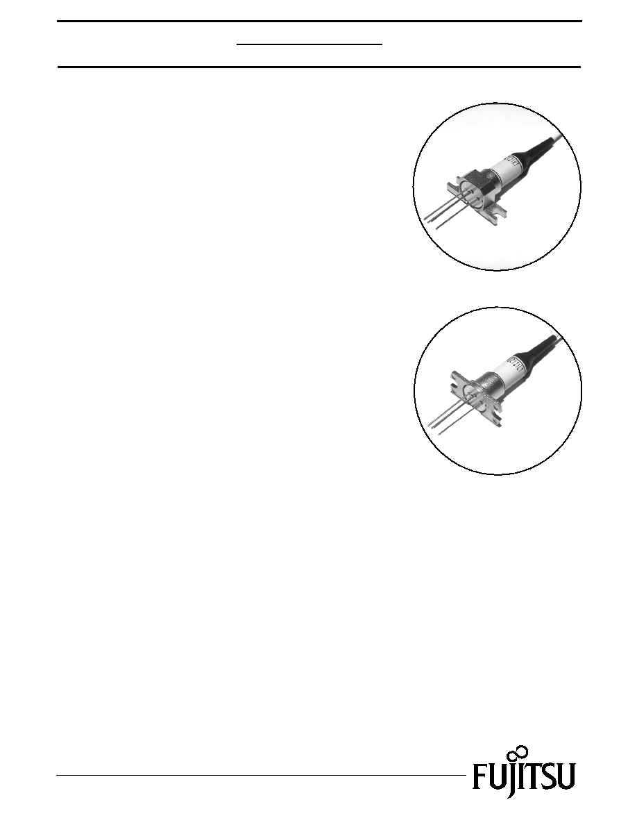
FEATURES
· Data rate up to 2.5Gb/s
· -23dBm typ. sensitivity
· 30µm active area PIN chip with GaAs pre-amplifier
· Small co-axial package with multi-mode fiber
APPLICATIONS
· High bit rate short haul optical transmission systems
operating at 2.5Gb/s
DESCRIPTION
These PIN preamplifiers use an InGaAs PIN chip with
GaAs IC preamplifier. The KT package is designed for a
horizontal PC board mount. The LT package is secured by a
vertical flange. Each package is connected with
multi-mode fiber by Nd: YAG welding. The detector
preamplifier is DC coupled and has a low electrical
output when the PIN is illuminated. These devices
are in compliance with ITU-T Recommendations
and meet Bellcore Requirements.
Edition 1.0
March 1999
1
InGaAs-PIN/Preamp
Receiver
FRM3Z231KT/LT
KT
LT

Edition 1.0
March 1999
2
InGaAs-PIN/Preamp
Receiver
FRM3Z231KT/LT
Parameter
PIN Responsivity
AC Transimpedance
Maximum Overload
Reverse Voltage
Symbol
R15
R13
OPTICAL & ELECTRICAL CHARACTERISTICS (Ta=-40° to +85°C, =1,310/1,550nm, Vss=-5.2V,
VR=5V, unless otherwise specified)
Zt
Bandwidth
Sensitivity
BW
Power Supply Current
Iss
Parameter
Storage Temperature
Operating Temperature
Supply Voltage
PIN Reverse Voltage
Symbol
Tstg
-40 to +85
-40 to +85
-7 to 0
0 to 20
V
V
°C
°C
Top
Vss
VR
PIN Reverse Current
2.0
mA
IR (Note 1)
Ratings
Unit
ABSOLUTE MAXIMUM RATINGS (Ta=25°C, unless otherwise specified)
Pr
VR
Po
A/W
A/W
dBm
mA
Unit
GHz
V
V
dBm
Limits
-
-
-21
20
Max.
0.80
0.80
-
1.8
400
-
-
-22
dBm
-
0
-
dBm
-
-3
-
-23
2.0
Equivalent Input
Noise Current Density
in
pA/ Hz
8
-
6.5
600
0.85
0.85
-
-
-
-
-
-5.2
40
-
5
Min.
Typ.
-22
-
Test Conditions
1,550nm, M=1
1,310nm, M=1
Power Supply Voltage
Vss
-4.94
-5.46
Ta=-40 to +85
°C
(Note 2)
Ta=-40 to +85
°C
2.488Gb/s NRZ,
PRBS=2
23
-1,
B.E.R.=10
-10
Ta=-40 to +85
°C
Ta=25
°C,
2.488Gb/s NRZ,
PRBS=2
23
-1,
B.E.R.=10
-10
AC-Coupled, RL=50
,
Average within BW
AC-Coupled, RL=50
,
Pin <-27dBm,
-3dBm from 1MHz
AC-coupled, f=100MHz,
RL=50
,
Pin <-20dBm
Note: (1) CW condition
(2) Maximum Input Optical Power, Pmax is defined as the optical power when the variation of F.W.H.M. of the output
waveform is less than 10% compared with that of the low input optical power level.
(3) Optical characteristics are specified on the condition that single mode fiber is used as the
optical source for testing.
(4) No data is available for either device.
Edition 1.0
March 1999
3
InGaAs-PIN/Preamp
Receiver
FRM3Z231KT/LT
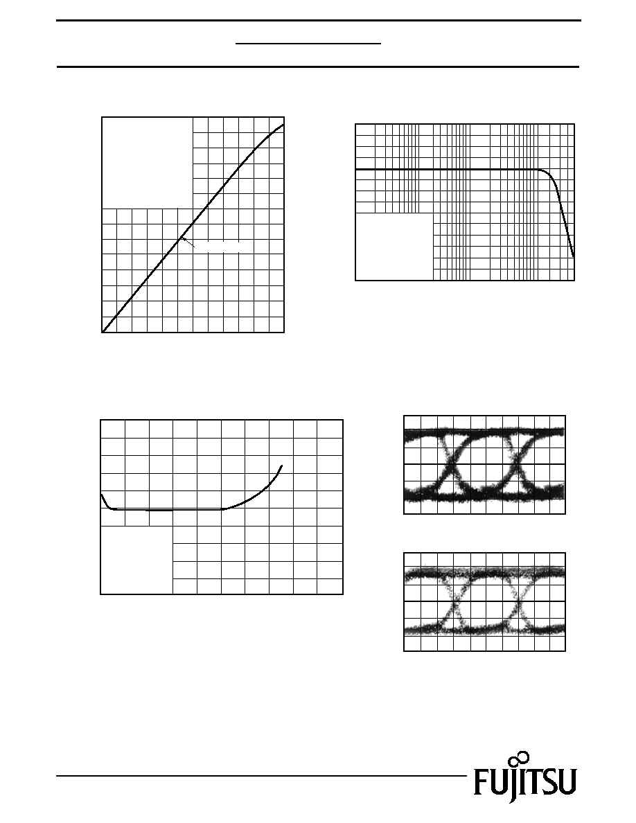
Fig. 2 Relative Frequency Response
Relative Response (3dB/div)
Frequency, f (MHz)
1000
100
10
1
Ta = 25°C
Vss=-5.2V
AC-Coupled
RL=
50
Pin=-30dBm
= 1,310/1,550nm
Fig. 1 Output Characteristics
Output Voltage Peak, Vpp(mV)
Average Photocurrent, Ip.ave (mA)
0.5
0.5
0.4
0.4
0.3
0.3
0.2
0.2
0.1
0.1
0
0
0.6
0.6
0.7
Zt ~ 600
Tc = 25°C
Vss=-5.2V
AC-Coupled
RL=
50
100Mb/s
Duty 50%
Mark density 50%
Fig.3 Equivalent Input Noise Current Density
Relative Input Noise Current Density,
in (pA/sqr. Hz)
Frequency, f (GHz)
2.0
1.0
0
0
5
10
Tc = 25°C
Vss=-5.2V
AC-Coupled
RL=
50
Fig.4 Eye Diagram with a 1,310nm,
2.5Gb/s NRZ, 2
23
-1 PRBS incident signal
100ps/div
Input optical wave form with Bessel filter
Equivalent output wave form at
Pin=-22dBm, Tc=25
°C, M=optimum
Edition 1.0
March 1999
4
InGaAs-PIN/Preamp
Receiver
FRM3Z231KT/LT
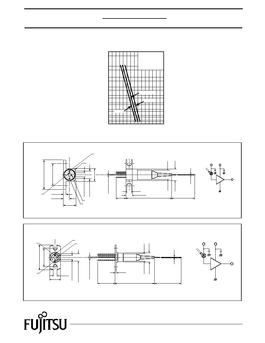
Fig.5 Bit Error Rate
Bit Error Rate
Received Optical Power (dBm)
-20
Ta=+25
°C
+85
°C
-40
°C
-25
-30
10
-12
10
-10
10
-8
10
-6
10
-4
=1,310/1,550nm
2.5Gb/s, NRZ
Vss=-5.2V
VR=
5V
2-C1.5
8.4
±0.2
8.4
±
0.2
4.2
±0.2
2.0
±0.1
14.0
±
0.15
17.0
±
0.2
VR
OUT
GND
VSS
10.0 MIN
2.5
±0.1
4.4 MAX
32.0 MAX
1000 MIN
4-
Ř
0.45
±
0.05
Ř
6.0 MAX
Ř
7.2 MAX
Ř
0.9
±
0.1
GND
VSS
VR
OUT
P.C.D. 4.0
±
0.2
P.C.D. 2.0
±
0.2
"KT" PACKAGE
7.6 MAX
2.5
±0.1
GND
VSS
VR
OUT
17.0
±
0.2
14.0
±
0.15
10.0 MIN
1.0
±0.1
32.0 MAX
1000 MIN
P.C.D. 4.0
±
0.2
4-
Ř
0.45
±
0.05
P.C.D. 2.0
±
0.2
Ř
6.0 MAX
Ř
7.2 MAX
Ř
0.9
VR
OUT
GND
VSS
"LT" PACKAGE
UNIT: mm
UNIT: mm

Edition 1.0
March 1999
5
InGaAs-PIN/Preamp
Receiver
FRM3Z231KT/LT
For further information please contact:
FUJITSU COMPOUND SEMICONDUCTOR, INC.
Americas & R.O.W.
2355 Zanker Rd.
San Jose, CA 95131-1138, U.S.A.
Phone: (408) 232-9500
FAX: (408) 428-9111
55 Schanck Road,
Suite A-2
Freehold, NJ 07728-2964, U.S.A.
Phone: (732) 303-0282
FAX: (732) 431-3393
www.fcsi.fujitsu.com
FUJITSU MIKROELECTRONIK GmbH
Quantum Devices Division
Network House
Norreys Drive
Maidenhead, Berkshire SL6 4FJ, UK
Phone:+44 (0)1628 504800
FAX:+44 (0)1628 504888
FUJITSU QUANTUM DEVICES, LTD.
Asia & Japan
2-7-1, Nishi Shinjuku
Shinjuku-ku, Tokyo 163-0721
Japan
Phone: 3-5322-3356
FAX: 3-5322-3398
Fujitsu Compound Semiconductor Products contain gallium arsenide
(GaAs) which can be hazardous to the human body and the environment.
For safety, observe the following procedures:
CAUTION
· Do not put this product into the mouth.
· Do not alter the form of this product into a gas, powder, or liquid
through burning, crushing, or chemical processing as these by-products
are dangerous to the human body if inhaled, ingested, or swallowed.
· Observe government laws and company regulations when discarding this
product. This product must be discarded in accordance with methods
specified by applicable hazardous waste procedures.
Fujitsu Limited reserves the right to change products and specifications without notice.
The information does not convey any license under rights of Fujitsu Limited or others.
© 1999 FUJITSU COMPOUND SEMICONDUCTOR, INC.
Printed in U.S.A. FCSI0199M200