FMM5804X
17.5-31.5GHz Power Amplifier MMIC
Item
Drain Voltage
Gate Voltage
Storage Temperature
Channel Temperature
Symbol
VDD
VGG
10
-3.0
-65 to +175
175
V
V
Input Power
Pin
16
dBm
°
C
°
C
Tstg
Tch
Operating Backside Temperature
-40 to +95
°
C
Top
Condition
Unit
Rating
ABSOLUTE MAXIMUM RATING (Ambient Temperature Ta=25
°
C)
Fujitsu recommends the following conditions for the long term reliable operation of GaAs FETs:
1. The drain-source operating voltage (VDD) should not exceed 6 volts.
2. The forward and reverse gate currents should not exceed 1.0 and -0.08 mA respectively.
3. This product should be hermetically packaged.
1
Edition 1.4
July 1999
Item
Symbol
Output Return Loss
RLo
Conditions
Unit
Limits
Typ.
Max.
Min.
ELECTRICAL CHARACTERISTICS (Ambient Temperature Tc=25
°
C)
Power Gain at 1 dB G.C.P.
15
18
-
-
-8
-
dB
Input Return Loss
RLi
-
-
-15
dB
dB
Frequency Range
f
17.5-31.5
GHz
Output Power at 1 dB G.C.P.
21**
23**
-
23*
25*
-
dBm
P
1dB
G
1dB
G.C.P.: Gain Compression Point
Power-Added Efficiency
-
18
-
%
add
Drain Current
-
300
400
mA
Iddrf
VDD = 6V
f = 17.5 ~ 31.5 GHz
*: at f = 17.5-30.0 GHz
IDD
=
250mA (Typ.)
ZS = ZL = 50
**: at f = 30.0-31.5 GHz
Note: RF parameter sample size 10pcs. Criteria (accept/reject)=(0/1)
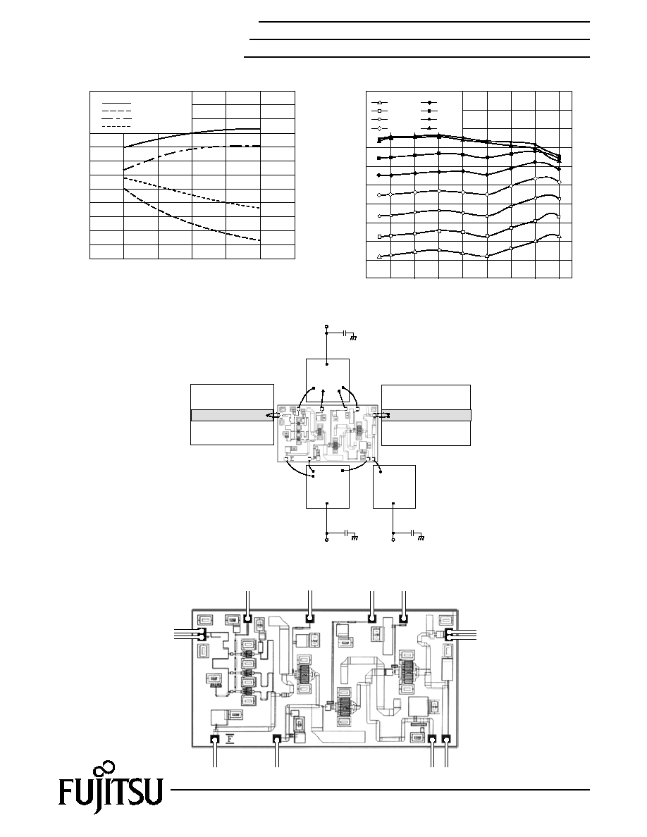
DESCRIPTION
The FMM5804X is a high-gain, wide band 4-stage
MMIC amplifier designed for operation in the 17.5-31.5 GHz
frequency range. This amplifier has an input and output
designed for use in 50
systems.This device is well
suited for point-to-point, point-to-multi-point(LMDS)
and satellite communication system applications.
FEATURES
· Output Power: (P1dB): 23.0dBm (Typ.)
· High Gain: (G1dB): 18dB (Typ.)
· High PAE:
add = 18% (Typ.)
· Wide Frequency Band: 17.5-31.5 GHz
· Impedance Matched Zin/Zout = 50
· 0.25µm PHEMT Technology

FMM5804X
17.5-31.5GHz Power Amplifier MMIC
4
For further information please contact:
FUJITSU COMPOUND SEMICONDUCTOR, INC.
2355 Zanker Rd.
San Jose, CA 95131-1138, U.S.A.
Phone: (408) 232-9500
FAX: (408) 428-9111
www.fcsi.fujitsu.com
FUJITSU QUANTUM DEVICES EUROPE, LTD.
Network House
Norreys Drive
Maidenhead, Berkshire SL6 4FJ
Phone:+44 (0)1628 504800
FAX:+44 (0)1628 504888
Fujitsu Limited reserves the right to change products and specifications without notice.
The information does not convey any license under rights of Fujitsu Limited or others.
© 1999 FUJITSU COMPOUND SEMICONDUCTOR, INC.
Printed in U.S.A. FCSI0599M200
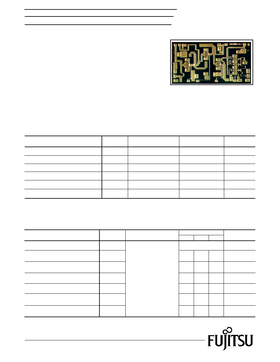
CHIP OUTLINE
Unit:
µ
m
0
0
0
2610
0
VGG1
Chip Size: 2610
±
30
µ
m x 1410
±
30
µ
m
Chip Thickness:70
±
20
µ
m
Pad Dimensions: 1. DC 80 x 80
µ
m
2. RF 120 x 80
µ
m
VGG2
VGG3
1140
1335
75
1140
1410
RFin
RFout
550
80
80
2530
1150
VGG4
1750
VDD3
2330
VDD2
840
VDD1
240
VDD4
2470
2050
Fujitsu Compound Semiconductor Products contain gallium arsenide
(GaAs) which can be hazardous to the human body and the environment.
For safety, observe the following procedures:
CAUTION
· Do not ingest.
· Do not alter the form of this product into a gas, powder, or liquid
through burning, crushing, or chemical processing as these by-products
are dangerous to the human body if inhaled, ingested, or swallowed.
· Observe government laws and company regulations when discarding this
product. This product must be discarded in accordance with methods
specified by applicable hazardous waste procedures.