N2ş1/1
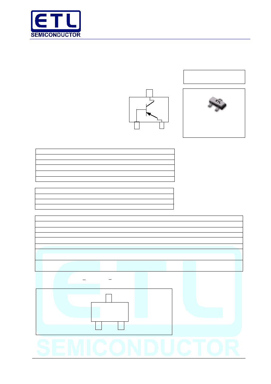
PNP General Purpose Amplifier
Transistor Surface Mount
CASE 318Dş03, STYLE1
SCş59
MAXIMUM RATINGS
(T
A
= 25 ░C)
Rating
Symbol
Value
Unit
Collector-Base Voltage
V
(BR)CBO
ş60
Vdc
Collector-Emitter Voltage
V
(BR)CEO
ş45
Vdc
Emitter-Base Voltage
V
(BR)EBO
ş7.0
Vdc
Collector Current - Continuous
I
C
ş100
mAdc
Collector Current - Peak
I
C(P)
ş200
mAdc
THERMAL CHARACTERISTICS
Characteristic
Symbol
Max
Unit
Power Dissipation
P
D
200
mW
Junction Temperature
T
J
150
░C
Storage Temperature
T
stg
ş55 ~ +150
░C
ELECTRICAL CHARACTERISTICS
(T
A
= 25 ░C)
Characteristic
Symbol
Min
Max
Unit
Collector-Emitter Breakdown Voltage (I
C
=ş2.0mAdc,I
B
=0)
V
(BR)CEO
ş45
--
Vdc
Collector-Base Breakdown Voltage (I
C
=ş10
Á
Adc,I
E
=0)
V
(BR)CBO
ş60
--
Vdc
Emitter-Base Breakdown Voltage (I
E
=ş10
Á
Adc,I
E
=0)
V
(BR)EBO
ş7.0
--
Vdc
Collector-Base Cutoff Current (V
CB
=ş45Vdc, I
E
=0)
I
CBO
--
ş0.1
Á
Adc
Collector-Emitter Cutoff Current (V
CE
=ş10Vdc, I
B
=0)
I
CEO
--
ş100
nAdc
DC Current Gain
(1)
h
FE1
210
340
--
(V
CE
=ş10Vdc, I
C
= ş2.0mAdc)
Collector-Emitter Saturation Voltage
V
CE(sat)
--
ş0.5
Vdc
(I
C
= ş100mAdc, I
B
=ş10mAdc)
1. Pulse Test: Pulse Width
300
Á
s, D.C.
2%.
DEVICE MARKING
Marking Symbol
The "X" represents a smaller alpha digit Date Code. The Date Code indicates the actual month
in which the part was manufactured.
COLLECTOR
3
2 1
BASE EMITTER
ARX
<
<
1
3
2
MSB709-RT1