+ 0.1
0 ~ 0.1
0.3 ~
0.6
(1) GND
(2) IN
(3) OUT
All terminals have same dimensions
+ 0.1
0 ~ 0.1
0.3 ~
0.6
(1) GND
(2) IN
(3) OUT
All terminals have same dimensions
P101/2
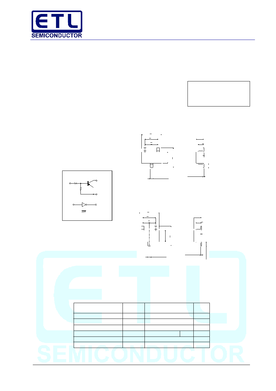
· Features
1) Built-in bias resistors enable the configuration of an inverter circuit without
connecting external input resistors (see equivalent circuit).
2) The bias resistors consist of thinfilm resistors with complete isolation to allow
positive biasing of the input. They also have the advantage of almost completely
eliminating parasitic effects.
3) Only the on/ off conditions need to be set for operation, making device design
easy.
· Structure
PNP digital transistor (with built-in resistors)
·Equivalent circuit
DTB143EK
DTB143EC
·
Absolute maximum ratings(T
a
=25
°C)
Parameter
symbol
limits
unit
Supply voltage
V
cc
50
V
Input voltage
V
IN
30~+10
V
Output current
I
C
500
mA
Power dissipation
P
d
200
300
mW
Junction temperature
T
j
150
°C
Storage temperature
T
stg
55~+150
°C
Digital transistors (built-in resistors)
2.9 + 0.2
1.9+ 0.2
0.95+ 0.95
(1)
(2)
(3)
+
0.2
1.6
- 0.1
2.8
+
0.2
+ 0.1
0.4
- 0.05
+ 0.1
0.15
- 0.06
+ 0.2
1.1
- 0.1
0.8 + 0.1
0 ~ 0.1
0.3 ~
0.6
(1) GND
(2) IN
(3) OUT
All terminals have same dimensions
2.9 + 0.2
1.9+ 0.2
0.95+ 0.95
(1)
(2)
(3)
+
0.2
1.3
- 0.1
2.4
+
0.2
+ 0.1
0.4
- 0.05
+ 0.1
0.15
- 0.06
+ 0.2
0.95
- 0.1
0.45 + 0.1
0 ~ 0.1
(1) GND
(2) IN
(3) OUT
All terminals have same dimensions
OUT
GND(+)
OUT
R1
R2
GND(+)
IN
IN
DTB143EK
DTB143EC
0.2Min
EIAJ: SC-- 59
EIAJ: SOT-- 23
P102/2
·
Elecrical characteristics(T
a
=25°C)
Parameter
symbol
Min.
Typ.
Max.
Unit
Conditions
Input voltage
V
I(off)
--
--
0.5
V
V
CC
= 5V, I
O
= 100
µ
A
V
I(on)
3
--
--
V
O
= 0.3V, I
O
=20mA
Output Voltage
V
O(on)
--
--
0.3
V
I
O
/ I
I
=50mA / 2.5mA
Input current
I
I
--
--
1.8
mA
V
I
= 5V
Output current
I
O(off)
--
--
0.5
µ
A
V
CC
= 50V,V
I
= 0 V
DC current gain
G
I
47
--
--
--
V
O
= 5V,I
O
= 50mA
Input resistance
R
1
3.29
4.7
6.11
K
--
Resistance ratio
R
2
/ R
1
0.8
1
1.2
--
--
Transition frequency
f
T
--
200
--
MHz
V
CE
= 10V, I
E
= 5 mA,f=100MHz*
*Transition frequency of the device
DTB143EK DTB143EC
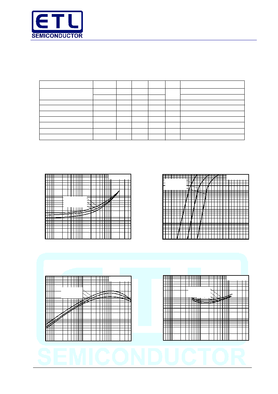
ELECTRICAL CHARACTERISTIC CURVES
INPUT VOL
T
AGE: V
I(on)
( V )
-100
-50
-20
-10
-5
-2
-1
-0.5
-0.2
-0.1
-100
µ
-200
µ
-500
µ
-1m
-2m
-5m
-10m -20m
-50m -100m
OUTPUT CURRENT: I
O
(A)
Figure 1. Input voltage vs.output current
(ON characteristics)
T
A
= 40°C
25°C
100°C
V
O
= 0.3V
OUTPUT CURRENT: I
O
( A )
-10m
-5m
-2m
-1m
-500
µ
-200
µ
-100
µ
-50
µ
-20
µ
-10
µ
-5
µ
-2
µ
-1
µ
0
0.5
1.0
1.5
2.0
2.5
3.0
INPUT VOLTAGE: V
I(ON)
(V)
Figure 2. Output current vs.input voltage
(OFF characteristics)
T
A
= 100°C
25°C
40°C
V
CC
= 5 V
DC CURRENT GAIN: G
I
1K
500
200
100
50
20
10
5
2
1
-100
µ
-200
µ
-500
µ
-1m
-2m
-5m
-10m -20m
-50m -100m
OUTPUT CURRENT: I
O
(A)
Figure 3. DC current gain vs.output current
V
O
= 5 V
T
A
= 100°C
25°C
40°C
OUTPUT VOL
T
AGE: V
O(on)
( V )
-1
-0.5
-0.2
-0.1
-0.05
-0.02
-0.01
-.005
-.002
-.001
-100
µ
-200
µ
-500
µ
-1m
-2m
-5m
-10m -20m
-50m -100m
OUTPUT CURRENT: I
O
(A)
Figure 4. Output voltage vs.output current
I
O
/ I
I
= 20
T
A
= 100°C
25°C
40°C