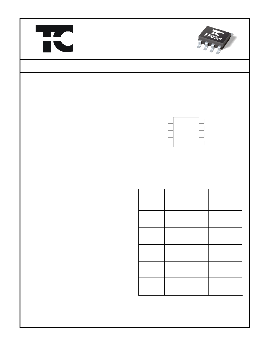
VRE4100 Series
Low Cost, SOIC-8
Precision References
DESCRIPTION
FEATURES
The VRE4100 is a low cost, high precision
bandgap reference that operates from +5V. The
device features low noise, digital error correction,
and an SOIC-8 package. The ultrastable output
is 0.05% accurate with a temperature coefficient
as low as 1.0 ppm/°C. The improvement in
overall accuracy is made possible by using
EEPROM registers and CMOS DAC's for
temperature and initial error correction. The DAC
trimming is done after assembly which eliminates
assembly related shifts.
The VRE4100 is recommended for use as a
reference for 14, 16, or 18 bit data converters
which require a precision reference. The
VRE4100 offers superior performance over
standard on-chip references commonly found
with data converters.
5
6
7
8
VRE4100
TOP
VIEW
1
2
3
4
NC
+V
IN
Enable
GND
NC
V
REF
NC
PIN CONFIGURATION
· 1.024, 1.250, 2.048, 2.500, 4.096V Output
· Initial Error: ± 0.05% max.
· Temperature Drift: 1.0 ppm/°C max.
· Low Noise: 2.2µV
p-p
(0.1Hz-10Hz, 1.024V)
· Low Thermal Hysterisis: 20ppm
· ±8mA Output Source
· Power Down Mode
· Industry Standard SOIC-8 pin out
· Commercial and Industrial Temp Ranges
· Second source for ADR29X, REF19X ,LT1460,
LT1461, LT1798, MAX616X, REF102
FIGURE 1
VRE4100DS REV. A MAY 01
SELECTION GUIDE
Model
Temp.
Range °C
Temp.
Coeff.
ppm/°C
VRE4110B
1.024
1.0
0°C to +70°C
VRE4110C
1.024 2.0
0°C
to
+70°C
VRE4110K
1.024 3.0
-40°C
to
+85°C
VRE4112B
1.250
1.0
0°C to +70°C
VRE4112C
1.250 2.0
0°C
to
+70°C
VRE4112K
1.250 3.0
-40°C
to
+85°C
VRE4120B
2.048
1.0
0°C to +70°C
VRE4120C
2.048 2.0
0°C
to
+70°C
VRE4120K
2.048 3.0
-40°C
to
+85°C
VRE4125B
2.500
1.0
0°C to +70°C
VRE4125C
2.500
2.0
0°C to +70°C
VRE4125K
2.500
3.0
-40°C to +85°C
VRE4141B
4.096
1.0
0°C to +70°C
VRE4141C
4.096 2.0
0°C
to
+70°C
VRE4141K
4.096 3.0
-40°C
to
+85°C
Output
Voltage
V
THALER CORPORATION · 2015 N. FORBES BOULEVARD · TUCSON, AZ. 85745 · (520) 882-4000
NC
www.thaler.com

160 235
I
L
= 8 mA
0.5 1.0
VRE4100B
± 0.025% ± 0.050%
VRE4100B
ppm/V
20 200
V
ref
+ 200mV V
IN
5.5V
V
OUT
/ V
IN
Line Regulation
(Note 6)
V
0.4
V
L
Logic Low Input Voltage
V
0.8
V
H
Logic High Input Voltage
nA
2
I
H
Logic High Input Current
nA
1
I
L
Logic Low Input Current
ppm
50
1000 Hours
V
OUT/T
Long Term Stability
µVp-p
2.2
0.1Hz<f<10Hz
E
n
Output Noise Voltage
(Note 4)
µs
2
To 0.01% of final value
T
ON
Turn-On Settling Time
mV
V
IN
-V
OUT
Dropout Voltage
(Note 3)
1.5 3.0
VRE4100K
1.0 2.0
VRE4100C
± 0.040% ± 0.080%
VRE4100C/K
%
V
OUT
Output Voltage Error
(Note 1)
ppm/mA
1 20
1mA I
Load
8mA
V
OUT
/ I
OUT
Load Regulation
(Note 6)
µA
230 320
V
load
= 0mA
I
IN
Supply Current
ppm
20
Note 5
Temperature Hysterisis
ppm/°C
TCV
OUT
Output Voltage
Temperature Coefficient
(Note 2)
V
1.8 5.5
V
IN
UNITS
MIN TYP MAX
SYMBOL
CONDITIONS
Input Voltage
PARAMETER
ELECTRICAL SPECIFICATIONS
Vps =+3V for VRE4110 and VRE4112, Vps =+5V for VRE4120, VRE4125 and VRE4141. T = 25°C, I
load
=1mA, C
out
=1µF unless otherwise noted.
Notes:
1.
High temperature and mechanical stress can effect the initial accuracy of the VRE4100 series
references.See discussion on output accuracy.
2.
The temperature coefficient is determined by the box method. See discussion on temperature
performance. All units are 100% tested over temperature.
3.
The minimum input to output differential voltage at which the output voltage drops by 0.5% from nominal.
4.
Based on 1.024V output. Noise is linearly proportional to V
REF.
5.
Defined as change in 25°C output voltage after cycling device over operating temperature range.
6.
Line and load regulation are measured with pulses and do not include output voltage changes due to self
heating.
VRE4100DS REV. A MAY 01
ABSOLUTE MAXIMUM RATINGS
Power supply to any input pin .......-0.3V to +5.6V
Output Short Circuit Duration .......................Indefinite
Operating Temp. (
B,C
) ....................0°C to 70°C
ESD Susceptibility Human Body Model.................2kV
Operating Temp. (
K
).....................-40°C to 85°C
ESD Susceptibility Machine Model ....................200V
Storage Temperature Range........-65°C to 150°C
Lead Temperature (soldering,10 sec)................260°C
www.thaler.com
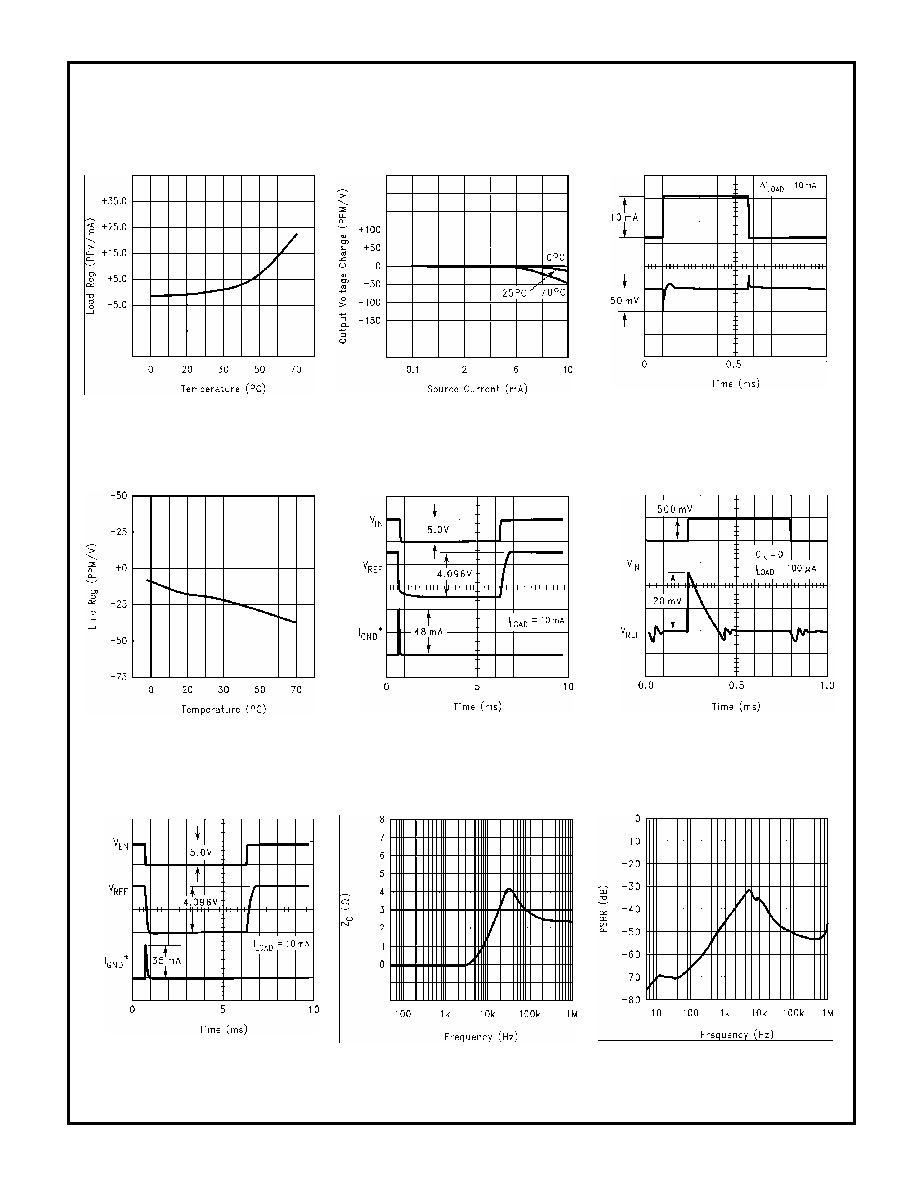
TYPICAL PERFORMANCE CURVES
VRE4100DS REV. A MAY 01
Load Regulation vs Temperature
Output Voltage vs Load Current
Line Transient Response
Load Transient Response
Line Regulation vs Temperature
Power Up/Down Ground Current
www.thaler.com
Enable Response
Output Impedance
Power Supply Rejection Ratio
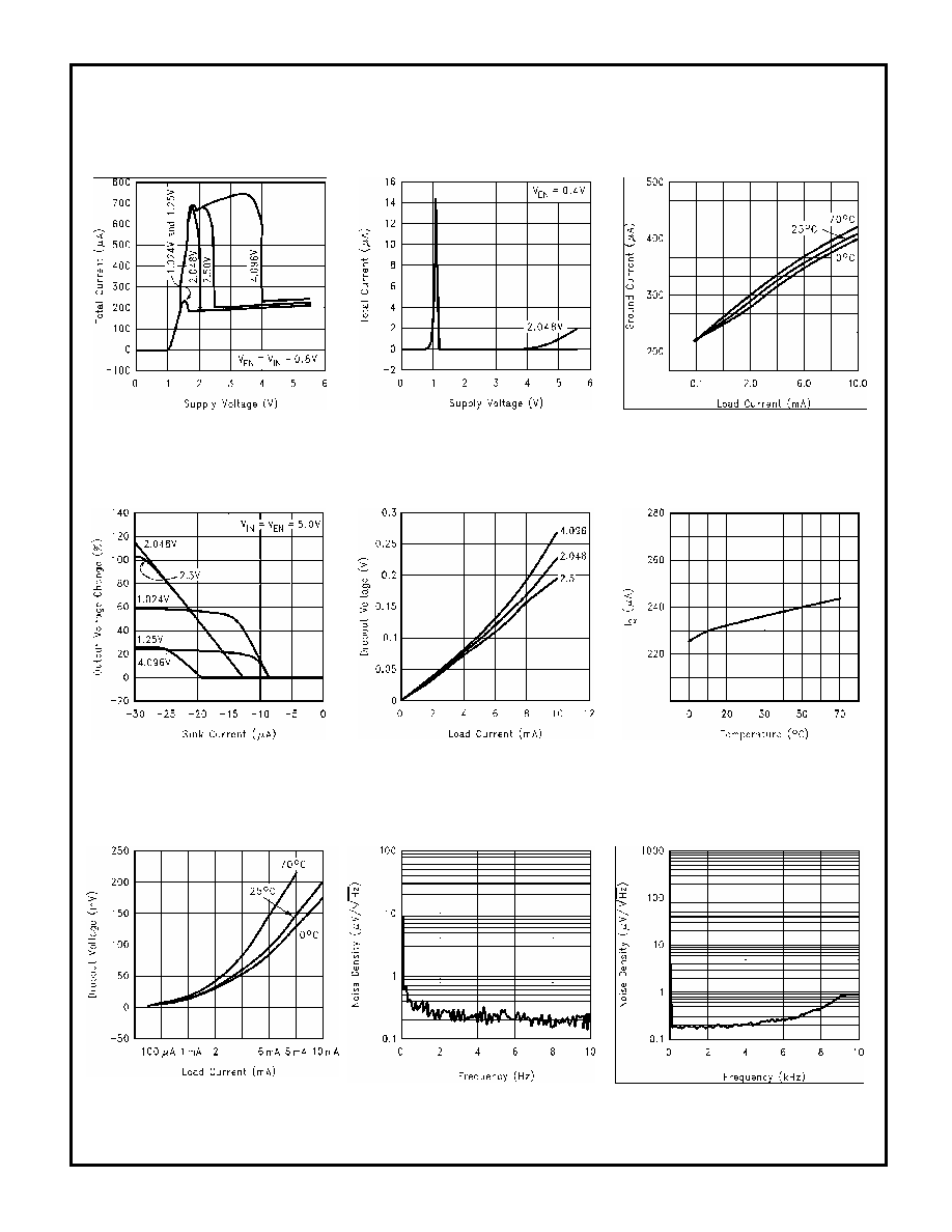
Total Current (Is
(ON)
) vs Supply Voltage
Total Current (Is
(OFF)
) vs Supply Voltage
Ground Current vs Load Current
TYPICAL PERFORMANCE CURVES
www.thaler.com
VRE4100DS REV. A MAY 01
Dropout Voltage vs Load Current
Output Voltage Change vs Sink Current I
(SINK)
I
Q
vs Temperature
Spectral Noise Density (0.1Hz to 10Hz)
Dropout Voltage vs Load Current (V
OUT
) = 2.0V
Spectral Noise Density (10Hz to 100kHz)
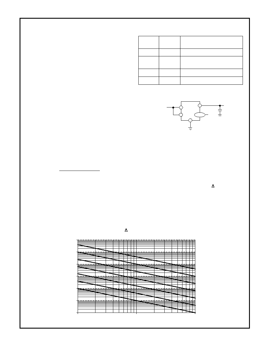
BASIC CIRCUIT CONNECTION
Figure 3 shows the proper connection of the
VRE4100 series voltage reference.
To achieve the specified performance, pay careful
attention to the layout. Commons should be
connected to a single point to minimize interconnect
resistances. This will reduce voltage errors, noise
pickup, and noise coupled from the power supply.
VRE4100DS REV. A MAY 01
Figure 2 External Connections
2
6
+ V
OUT
3
+ V
IN
VRE4100
NC
Enable
4
C
OUT
1µF
Reference output
Vout
6
This pin must be left open
NC
1,5,7,8
Pulled to V
in
for normal
operation.
Enable
3
Positive power supply input
These must be connected to
ground
Vin
GND
2
4
PIN DESCRIPTION
www.thaler.com
TEMPERATURE PERFORMANCE
The VRE4100 is designed for applications where
the initial error at room temperature and drift over
temperature are important to the user. For many
instrument manufacturers, a voltage reference with
a temperature coefficient of 1ppm/°C makes it
possible to eliminate a system temperature
calibration, a slow and costly process.
Of the three TC specification methods (slope,
butterfly, and box), the box method is most
commonly used. A box is formed by the min/max
limits for the nominal output voltage over the
operating temperature range. The equation follows:
This method corresponds more accurately to the
method of test and provides a closer estimate of
actual error than the other methods. The box
method guarantees limits for the temperature error
but does not specify the exact shape or slope of the
device under test.
For example a designer who needs a 14-bit
accurate data acquisition system over the industrial
temperature range (-40°C to +85°C), will need a
voltage reference with a temperature coefficient
(TC) of 1.0ppm/°C if the reference is allowed to
contribute an error equivalent to 1LSB. Figure 3
shows the required reference TC vs. T change from
25°C for resolution ranging from 8 bits to 20 bits.
0.01
0.1
1
10
100
1000
10000
1
10
100
20 BIT
18 BIT
16 BIT
14 BIT
12 BIT
10 BIT
8 BIT
ReferenceTC
(ppm/°C)
Figure 3 Reference TC vs. T change from 25°C for 1 LSB change
1,5,7,8
)
10
(
)
(
.
.
6
min
max
min
min
max
T
T
V
V
V
C
T
al
no
-
-
=