- 1 -
NEL
MD-01-4-43-75-482
May 8, 2002
Preliminary
MC740-430E
47-Gb/s 4:1 Multiplexer
The MC740-430E is an engineering sample of 47-Gb/s signal generator. It consists of a 4:1
multiplexer (MUX), D-type flipflop (D-FF), and clock distribution unit based on 0.1-
µm InP-HEMT
devices. Four-parallel data inputs are multiplexed to 47-Gb/s data by using 47- and 11.75-GHz
clock signals. At the output stage, the D-FF regenerates the muliplexed data with the 47-GHz clock
signal and offers symmetrical eye openings. The MC740-430E has SCFL (Source Coupled FET
Logic) I/O and can be directly connected to a pulse pattern generator.
FEATURES
Operating range:
38 to 47 Gb/s (min.)
(note)
Signal regeneration with full-rate clock signal
Large output amplitude:
SCFL I/O (V
OHD
= 0V, V
OLD
= -0.9V, typ.)
Single power supply voltage:
DC -6 V
(note) 50-Gb/s operation is optional.
APPLICATIONS
Parallel-to-serial converters, Test equipments
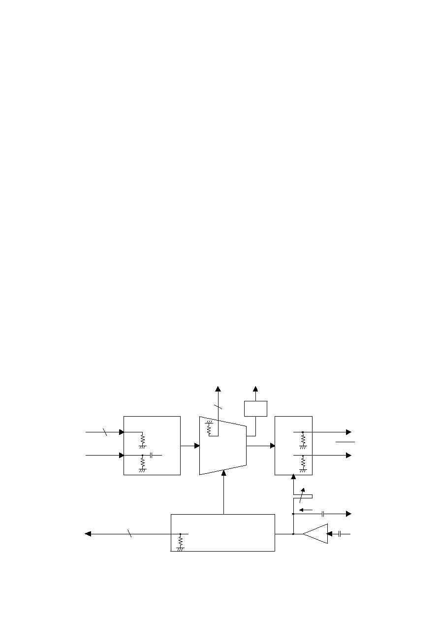
FUNCTION DIAGRAM
Fig. 1. Function diagram.
Latching stage
4:1 MUX
50
50
75
10-dB
ATT
75
75
50
Clock Distributor
65
DATA 3, 2, 1, 0
4
2
CLK10
CLK10
DATA
DATA
CLK40
CLK40
40Gb/s
(mon.)
20Gb/s
(mon.)
shifter
50
D-FF
2
- 2 -
NEL
MC740-430E
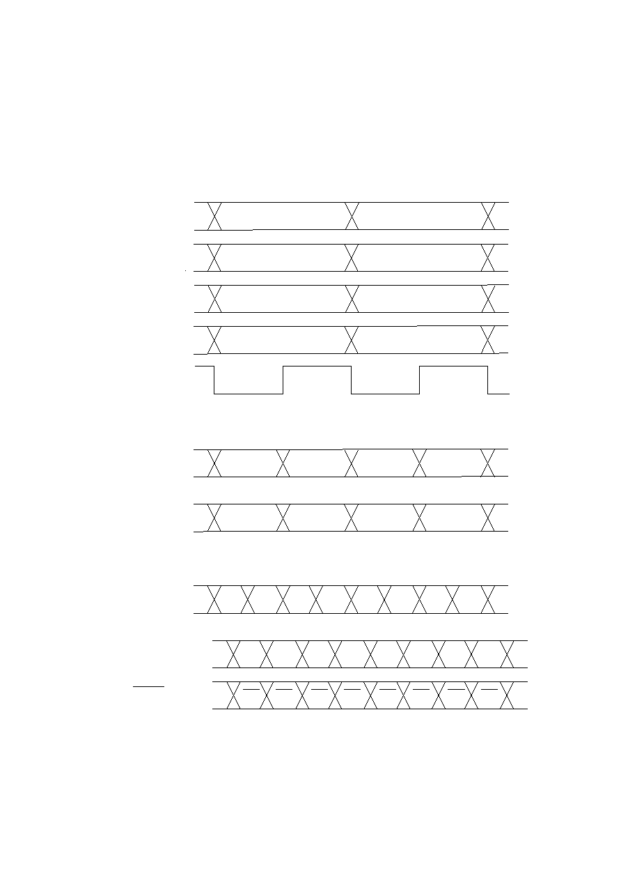
TIMING CHARTS
D3
0
D2
0
D1
0
D0
0
D3
1
D2
1
D1
1
D0
1
D3
0
D2
0
D1
0
D0
0
D3
1
D2
1
D1
1
D0
1
D3
0
D1
0
D3
1
D1
1
D2
0
D0
0
D2
1
D0
1
D3
1
D3
0
D2
1
D2
0
D1
1
D1
0
D0
1
D0
0
D3
0
D2
0
D1
0
D0
0
D3
1
D2
1
D1
1
D0
1
(1) Data and Clock Input Signals
(2) Multiplexed 20 Gb/s Data Output Signals (Monitor)
(3) Multiplexed 40 Gb/s Data Output Signals
DATA
40 Gb/s
(4:1 MUX output)
DATA3
DATA2
DATA1
DATA0
CLK10
20 Gb/s
Odd ch.
DATA
20 Gb/s
Even ch.
Fig. 2. Timing charts.
- 3 -
NEL
MC740-430E
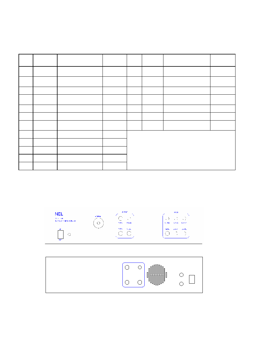
CONNECTION TABLE
No. NAME
FUNCTION
TERM-
INAL
No. NAME
FUNCTION
TERM-
INAL
1
Front
Switch
Front Switch
-
13
20Gb/s
Even
20G Monitor
(Even ch., DATA2 and 0)
K(f)
(2)
2
shifter
Clock Phase Shifter
for D-FF
-
14
20Gb/s
Odd
20G Monitor
(Odd ch., DATA3 and 1)
K(f)
(2)
3 DATA
Data Output
V(f)
(1)
15 CLK10
1/4 Clock Output SMA(f)
4 /DATA
Data Output
(complement)
V(f)
(1)
16 40Gb/s
40G Monitor
(4:1 MUX Output)
V(f)
(1)
5 CLK10
1/4 Clock Output
SMA(f)
17 PWR
Power Supply (-6.0 V)
-
6 CLK40
Clock Output
V(f)
(1)
18 GND
Ground (0.0 V)
-
7 CLK10
1/4 Clock Input
SMA(f)
19
Main
Switch
Main Switch
-
8 CLK40
Clock Input
V(f)
(1)
9 DATA3
Data Input 3
SMA(f)
10 DATA1
Data Input 1
SMA(f)
11 DATA2
Data Input 2
SMA(f)
12 DATA0
Data Input 0
SMA(f)
notes) (1) V: Anritsu panel adaptor V232
(2) K: Anritsu panel adaptor K232B
CONNECTION DIAGRAM
FRONT PANEL
REAR PANEL
ON
OFF
CLK10
20Gb/s
Odd
GND
-6V DC
40Gb/s
Even
MONITOR
Fig. 3. Front and rear panels.
Case dimension (without connectors)
height: 95 mm
width: 370 mm
depth: 235 mm
1
3
4
5
6
2
11
9
10
12
7
8
13
14
15
16
19
18
17
- 4 -
NEL
MC740-430E
ABSOLUTE MAXIMUM RATINGS
GENERAL
SYMBOL
PARAMETER Ratings
V
PWR
Power Supply Voltage
TBD
Tstor
Storage Temperature
TBD
DATA and CLOCK INPUT SIGNALS
SYMBOL
PARAMETER Ratings
DATA3 to 0
Applied Voltage at DATA3 to 0
-1.9 to 0 V
V
ICLK40
Applied Voltage at CLK40
-1.6 to +1.6 V (DC), 1.6 Vpp (AC)
V
ICLK10
Applied Voltage at CLK10
-1.6 to +1.6 V (DC), 1.6 Vpp (AC)
DATA and CLOCK OUTPUT SIGNALS
SYMBOL
PARAMETER Ratings
V
DATA, /DATA
Applied Voltage at DATA, /DATA
TBD
V
OC40
Applied Voltage at CLK40
-1.2 to 1.2 V (DC), No RF Input
V
OC10
Applied Voltage at CLK10
-1.75 to +0.2 V
MONITOR OUTPUT SIGNALS
SYMBOL
PARAMETER Conditions
40Gb/s
40-Gb/s Monitor Output Interface
TBD
20Gb/s
(
odd, even)
20-Gb/s Monitor Output Interface
-1.75 to +0.2 V
CLK10
10-GHz Clock Output Interface
-1.75 to +0.2 V
- 5 -
NEL
MC740-430E
RECOMMENDED OPERATING CONDITIONS
GENERAL
SYMBOL
PARAMETER MIN.
TYP.
MAX.
UNITS
V
PWR
(note1)
Power Supply Voltage
-6.0 V
Ta
(note2)
Operating Temperature
20
-
30
(note1)
NEL recommends a DC power supply with an output current capacity of 10 A and an output voltage
ripple less than 10 mV rms.
(note2)
The MC740-430E should be protected from condensation.
DATA and CLOCK INPUT SIGNALS
SYMBOL
PARAMETER Conditions
DATA3 to 0
Data Input Interface
DC coupling
(see DC and AC characteristics)
CLK40
40-GHz Clock Input Interface
(with an internal DC blocking capacitor)
AC coupling
(see AC characteristics)
CLK10
10-GHz Clock Input Interface
AC or DC coupling
(see AC characteristics)
DATA and CLOCK OUTPUT SIGNALS
SYMBOL
PARAMETER Conditions
DATA,
/DATA
Data Output Interface
DC coupling,
Terminate with 50
to GND
CLK40
40-GHz Clock Output Interface
(with an internal DC blocking capacitor)
AC coupling,
Terminate with 50
CLK10
10-GHz Clock Output Interface
AC or DC coupling,
Terminate with 50
MONITOR OUTPUT SIGNALS
SYMBOL
PARAMETER Conditions
40Gb/s
40-Gb/s Monitor Output Interface
(with an internal 10-dB attenuator)
DC coupling,
Terminate with 50
to GND
20 Gb/s
(
odd, even)
20-Gb/s Monitor Output Interface
DC coupling,
Terminate with 50
to GND
CLK10
10-GHz Clock Output Interface
AC or DC coupling,
Terminate with 50