Äîêóìåíòàöèÿ è îïèñàíèÿ www.docs.chipfind.ru
EUA5202
DS5202 Ver 1.4 Nov. 2004
1
2-W Stereo Audio Power Amplifier
with Mute
DESCRIPTION
The EUA5202 is a stereo audio power amplifier that
delivering 2W of continuous RMS power per channel
into 3- loads. When driving 1W into 8- speakers, the
EUA5202 has less than 0.04% THD+N across its
specified frequency range. Included within this device is
integrated de-pop circuitry that virtually eliminates
transients that cause noise in the speakers.
Amplifier gain is externally configured by means of two
resistors per input channel and does not require external
compensation for settings of 2 to 20 in BTL mode (1 to
10 in SE mode). An internal input MUX allows two sets
of stereo inputs to the amplifier. In notebook
applications, where internal speakers are driven as BTL
and the line (often headphone drive) outputs are required
to be SE, the EUA5202 automatically switches into SE
mode when the
BTL
SE/
inputs is activated. Consume
only 7mA of supply current during normal operation,
and the EUA5202 also features a shutdown function for
power sensitive applications, holding the supply current
at 1µA.
FEATURES
Output Power at 3
Load
- 2W/ch at V
DD
=5V
- 800mW/ch at 3V
Low Supply Current and Shutdown Current
Integrated Depop Circuit
Mute and Shutdown Control Function
Thermal Shutdown Protection
Stereo Input MUX
Bridge-Tied Load (BTL) or Single-Ended (SE)
Modes.
TSSOP-24 with Thermal Pad
APPLICATIONS
Notebook Computers
Multimedia Monitors
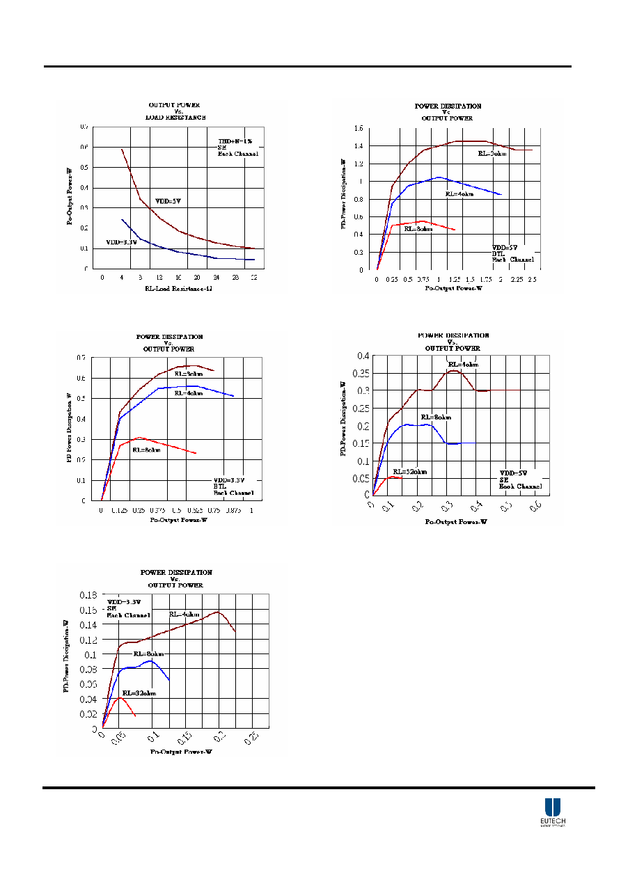
Digital Radios and Portable TVs
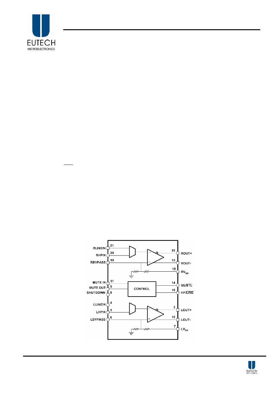
Block Diagram
EUA5202
DS5202 Ver 1.4 Nov. 2004
2
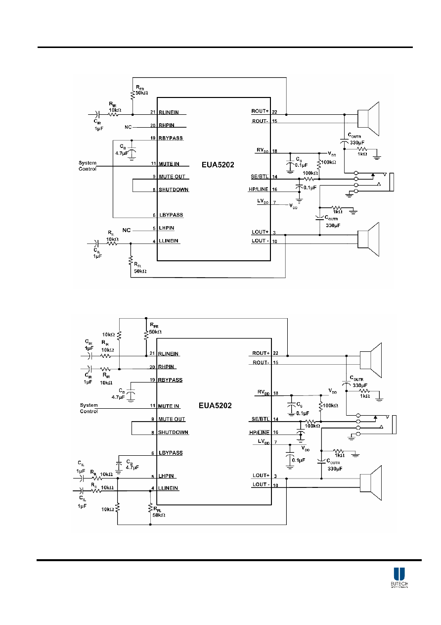
Typical Application Circuit
Figure 1. EUA5202 Minimum Configuration Application Circuit
Figure 2. EUA5202 Full Configuration Application Circuit
EUA5202
DS5202 Ver 1.4 Nov. 2004
3
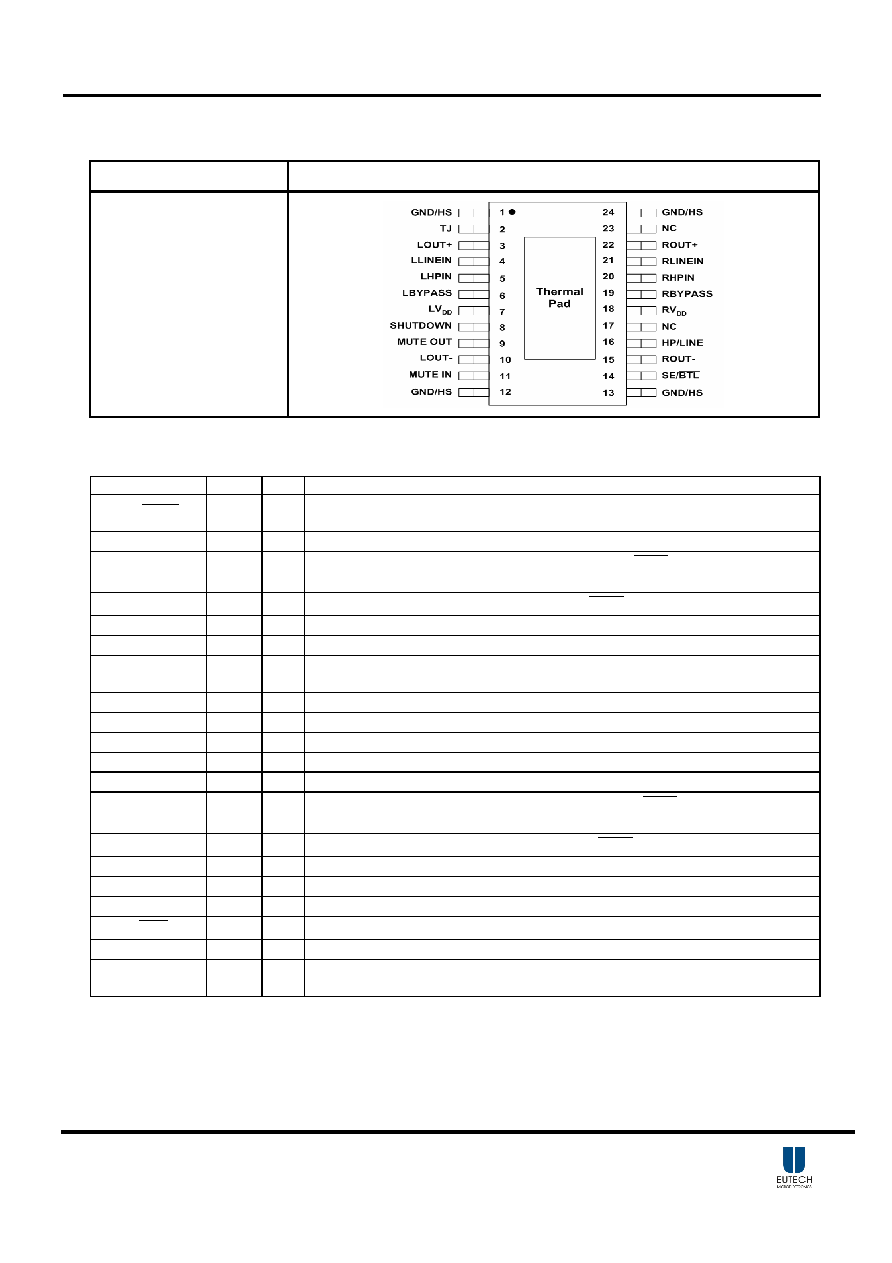
Pin Configurations
Package Pin
Configurations
TSSOP-24 with Thermal
Pad,
exposure on the bottom
of the package
Pin Description
PIN
PIN
I/O
DESCRIPTION
LINE
HP/
16 I
Input MUX control input, hold high to select LHP IN or RHP IN (5, 20), hold
low to select LLINE IN or RLINE IN (4, 21)
LBYPASS
6
Tap to voltage divider for left channel internal mid-supply bias
LHPIN 5
I
Left channel headphone input, selected when
LINE
HP/
terminal (16) is held
high
LLINE IN
4
I
Left channel line input, selected when
LINE
HP/
terminal (16) is held low
LOUT+
3
O
Left channel + output in BTL mode, + output in SE mode
LOUT-
10
O
Left channel - output in BTL mode, high-impedance state in SE mode
GND/HS
1,12,13,
24
Ground connection for circuitry, directly connected to thermal pad
LV
DD
7
I
Supply voltage input for left channel and for primary bias circuits
MUTE IN
11
I
Mute all amplifiers, hold low for normal operation, hold high to mute
MUTE OUT
9
O
Follows MUTE IN terminal (11), provides buffered output
NC
17,23
No internal connection
RBYPASS
19
Tap to voltage divider for right channel internal mid-supply bias
RHPIN 20
I
Right channel headphone input, selected when
LINE
HP/
terminal (16) is held
high
RLINEIN 21 I
Right channel line input, selected when
LINE
HP/
terminal (16) is held low
ROUT+
22
O
Right channel + output in BTL mode, + output in SE mode
ROUT-
15
O
Right channel - output in BTL mode, high-impedance state in SE mode
RV
DD
18
I
Supply voltage input for high channel
BTL
SE/
14
I
Hold low foe BTL mod, hold high for SE mode
SHUTDOWN
8
I
Places entire IC in shutdown mode when held high, I
DD
=5µA
T
J
2
O
Sources a current proportional to the junction temperature. This terminal should
be left unconnected during normal operation.
EUA5202
DS5202 Ver 1.4 Nov. 2004
4
Ordering Information
Order Number
Package Type
Marking
Operating Temperature range
EUA5202QIR TSSOP
24
xxxx
EUA5202
-40°C to 85°C
EUA5202QIT TSSOP
24
xxxx
EUA5202
-40°C to 85°C
EUA5202
Packing
R: Tape& Reel
T: Tube
Operating temperature range
I: Industry Standard
Package Type
Q: TSSOP
EUA5202
DS5202 Ver 1.4 Nov. 2004
5
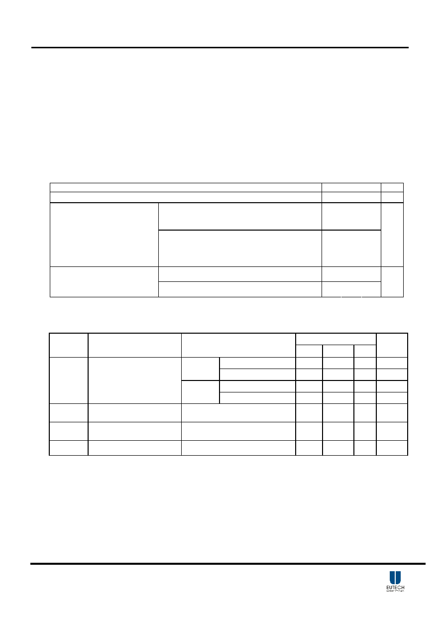
Absolute Maximum Ratings
Supply voltage , V
DD
------------------------------------------------------------------------------------------- 6V
Input voltage, V
1
---------------------------------------------------------------------------- -0.3V to V
DD
+0.3V
Continuous total power dissipation------------------------------------------------------------- internally limited
Operating free-air temperature range ,T
A
------------------------------------------------------- 40°C to 85°C
Operating junction temperature range, T
J
------------------------------------------------------- 40°C to 150°C
Storage temperature range, T
stg
---------------------------------------------------------------- 65°C to 150°C
Lead temperature 1,6 mm (1/16 inch) from case for 10 seconds-------------------------------------- 260°C
Recommended Operating Conditions
MIN NOM MAX UNIT
Supply Voltage, V
DD
3 5 5.5
V
V
DD
= 5V,
250m W/Ch average
power,
4-
stereo BTL drive,
with proper PCB design -40 85
Operating free-air temperature,
T
A
V
DD
= 5V,
2 W/Ch average power,
3-
stereo BTL drive,
with proper PCB design
and 300 CFM
forced-air cooling
-40 85
°C
V
DD
= 5V
1.25 4.5
Common mode input voltage,
V
ICM
V
DD
= 3.3V
1.25 2.7
V
DC Electrical Characteristics, T
A
=25°C
EUA5202
Symbol Parameter
Conditions
Min. Typ Max.
Unit
Stereo BTL
7.1
11
mA
V
DD
=5V
Stereo SE
3.9
6
mA
Stereo BTL
5.7
9
mA
I
DD
Supply
Current
V
DD
=3.3V
Stereo SE
3.1
5
mA
V
OO
Output
Offset
Voltage
(measured differentially)
V
DD
=5V, Gain=2
5
25
mV
I
DD (Mute)
Supply Current in Mute
Mode
V
DD
=5V
1.55
mA
I
DD(SD)
I
DD
in Shutdown
V
DD
=5V
1
5
µA
EUA5202
DS5202 Ver 1.4 Nov. 2004
6
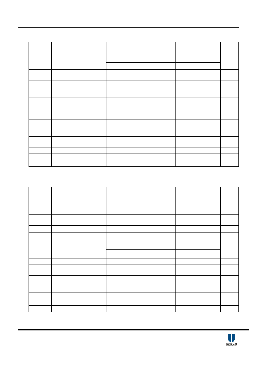
Typical Ac Operating Characteristics, V
DD
=5V, T
A
=25°C, R
L
=3
Symbol Parameter
Conditions
Typ. Unit
THD=0.2%, BTL, See Figure 3
2
P
O
Output Power(each
channel)
*1
THD=1%, BTL, See Figure 3
2.2
W
THD+N
Total Harmonic Distortion
Plus Noise
P
O
=2W, f=1KHz ,See Figure5
200
m%
V
1
=1V, R
L
=10k, A
V
=1V/V 100
m%
B
OM
Maximum Output Power
Bandwidth
AV=10V/V THD <1%, See Figure5
>20 KHz
f=1KHz, See Figure37
65
Supply Ripple Rejection
Ratio
f=20-20KHz, See Figure37
40
dB
Mute
Attenuation
85 dB
Channel-to- Channel Output
Separation
f=1KHz, See Figure 39
85
dB
Line/HP Input Separation
88
dB
BTL Attenuation in SE
Mode
86
dB
Z
1
Input
Impedance
2
M
Signal-to-Noise
Ratio
P
O
=2W,BTL, 5V
101
dB
V
N
Output Noise Voltage
See Figure 35
22
µV(rms)
*1: Output Power is measured at the output terminals of the IC at 1 KHz
Typical Ac Operating Characteristics, V
DD
=3.3V, T
A
=25°C, R
L
=3
Symbol Parameter
Conditions
Typ. Unit
THD=0.2%, BTL, See Figure 10
800
P
O
Output Power(each
channel)
*1
THD=1%, BTL, See Figure 10
900
W
THD+N
Total Harmonic Distortion
Plus Noise
P
O
=2W, f=1KHz ,See Figure11
350
m%
V
1
=1V, R
L
=10k, A
V
=1V/V 200 m%
B
OM
Maximum Output Power
Bandwidth
AV=10V/V THD <1%, See Figure11
>20
KHz
f=1KHz, See Figure37
60
Supply Ripple Rejection
Ratio
f=20-20KHz, See Figure37
40
dB
Mute
Attenuation
85 dB
Channel-to- Channel Output
Separation
f=1KHz, See Figure 40
80
dB
Line/HP Input Separation
88
dB
BTL Attenuation in SE
Mode
86
dB
Z
1
Input
Impedance
2
M
Signal - to - Noise Ratio
P
O
=700mW,BTL, 5V
96
dB
V
N
Output Noise Voltage
See Figure 36
22
µV(rms)
*1: Output Power is measured at the output terminals of the IC at 1 KHz
EUA5202
DS5202 Ver 1.4 Nov. 2004
7
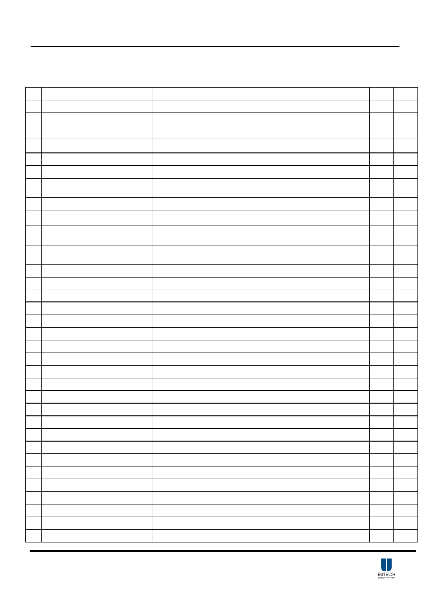
Typical Operating Characteristics
(Table of Graphs)
No
Item Conditions
Figure Page
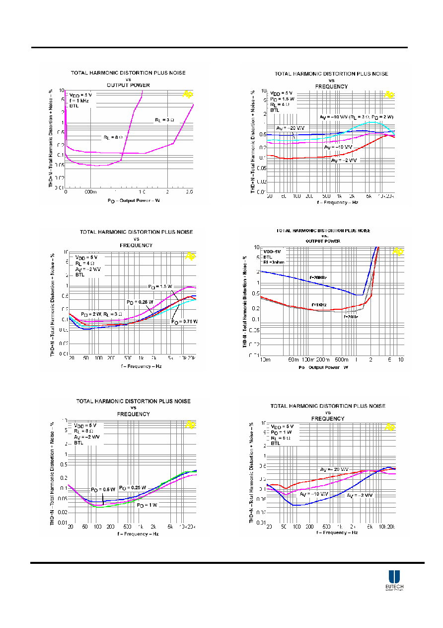
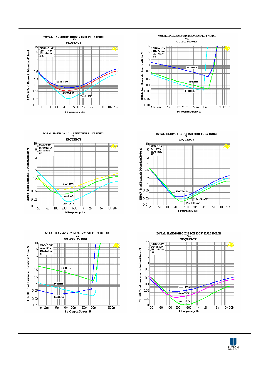
1
THD+N vs. Output Power
VDD=5VRL=3 & 8 ohmBTLf=1KHz
3
9
2
THD+N vs. Frequency
VDD=5VRL=4 ohmBTLPo=1.5W
f=20 to 20KHzAv= -2 & -10 & -20V/V
4
9
3
THD+N vs. Frequency
VDD=5VRL=3 & 4 ohmBTLPo=1.5W f=20 to 20KHz
5
9
4
THD+N vs. Output Power
VDD=5VRL=3 ohmBTLf=20 & 1K & 20KHz
6
9
5
THD+N vs. Frequency
VDD=5VRL=8 ohmBTLf=20 to 20KHzAv=-2V/V
7
9
6
THD+N vs. Output Power
VDD=5VRL=8 ohmBTLPo=1W Av= -2 &-10 & -20V/Vf=20
to 20KHz
8
9
7
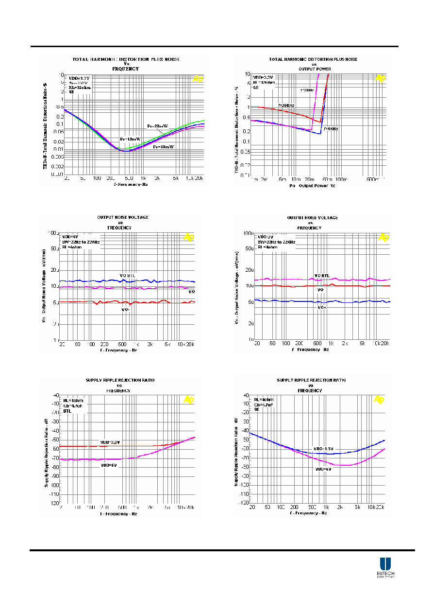
THD+N vs. Output Power
VDD=5VRL=8 ohmBTLf=20 & 1K & 20KHz
9
10
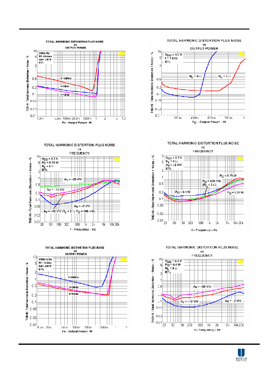
8
THD+N vs. Output Power
VDD=3.3VRL=3 & 8 ohmBTLf=1KHz
10
10
9
THD+N vs. Frequency
VDD=3.3VRL=4 ohmBTLPo=0.75WAv= -2 &-10 &-20V/V
f=20 to 20KHz
11
10
10
THD+N vs. Frequency
VDD=3.3VRL=4 ohmBTLAv=-2V/V Po=0.1 & 0.35 & 0.75W
& 800mW(RL=3 ohm)
12
10
11
THD+N vs. Output Power
VDD=3.3VRL=3 ohmBTLAv=-2V/Vf=20 & 1K & 20KHz
13
10
12
THD+N vs. Frequency
VDD=3.3VRL=8 ohmBTLPo=0.4W Av=-2 &-10 & -20V/V
14
10
13
THD+N vs. Frequency
VDD=3.3VRL=8 ohmBTLAv=-2V/V Po=0.1 & 0.25 & 0.4W
15
11
14
THD+N vs. Output Power
VDD=3.3VRL=8 ohmBTLAv= -2V/Vf=20 & 1K &20KHz
16
11
15
THD+N vs. Frequency
VDD=5VRL=4 ohmSEPo=0.5WAv= -1&-5&-10V/V
17
11
16
THD+N vs. Frequency
VDD=5VRL=4 ohmSEAv= -2V/VPo=0.1 & 0.25 & 0.5W
18
11
17
THD+N vs. Output Power
VDD=5VRL=4 ohmSEAv= -2V/Vf=100 & 1K & 20KHz
19
11
18
THD+N vs. Frequency
VDD=5VRL=8 ohmSEPo=0.25WAv= -1 &-5 &-10V/V
20
11
19
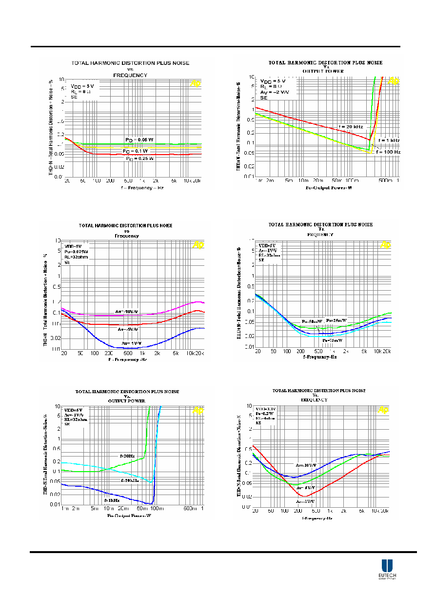
THD+N vs. Frequency
VDD=5VRL=8 ohmSEAv= -2V/VPo=0.05 & 0.1 & 0.25W
21
12
20
THD+N vs. Output Power
VDD=5VRL=8 ohmSEAv= -2V/Vf=100 &1K & 20KHz
22
12
21
THD+N vs. Frequency
VDD=5VRL=32 ohmSEPo=0.075WAv= -1 &-5 &-10V/V
23
12
22
THD+N vs. Frequency
VDD=5VRL=32 ohmSEAv= -1V/VPo=25 & 50 & 75mW
24
12
23
THD+N vs. Output Power
VDD=5VRL=32 ohmSEAv= -1V/Vf=20 & 1K & 20KHz
25
12
24
THD+N vs. Frequency
VDD=3.3VRL=4 ohmSEPo=0.2WAv= -1 &-5 &-10V/V
26
12
25
THD+N vs. Frequency
VDD=3.3VRL=4 ohmSEAv= -1V/VPo=0.05 & 0.1 & 0.2W
27
13
26
THD+N vs. Output Power
VDD=3.3VRL=4 ohmSEAv= -2V/Vf=100 & 1K & 20KHz
28
13
27
THD+N vs. Frequency
VDD=3.3VRL=8 ohmSEPo=100mWAv= -1 &-5 &-10V/V
29
13
28
THD+N vs. Frequency
VDD=3.3VRL=8 ohmSEAv= -1V/VPo=25 & 50 &100mW
30
13
29
THD+N vs. Output Power
VDD=3.3VRL=8 ohmSEAv= -1V/Vf=100 & 1K & 20KHz
31
13
30
THD+N vs. Frequency
VDD=3.3VRL=32 ohmSEPo=30mWAv= -1 &-5 &-10V/V
32
13
31
THD+N vs. Frequency
VDD=3.3VRL=32 ohmSEAv= -1V/VPo=10 & 20 & 30mW
33
14
32
THD+N vs. Output Power
VDD=3.3VRL=32 ohmSEAv=-1V/Vf=20 & 1K & 20KHz
34
14
EUA5202
DS5202 Ver 1.4 Nov. 2004
8
33
Output Noise Voltage vs. Frequency VDD=5VBW=22Hz to 22kHzRL=4
35
14
34
Output Noise Voltage vs. Frequency VDD=3.3VBW=22Hz to 22kHzRL=4
36
14
35
Supply Ripple Rejection Ratio vs.
Frequency
RL=4 ohmCB=4.7uFBTLVDD=3.3 & 5V
37
14
36
Supply Ripple Rejection Ratio vs.
Frequency
RL=4 ohmCB=4.7uFSEVDD=3.3 & 5V
38
14
37
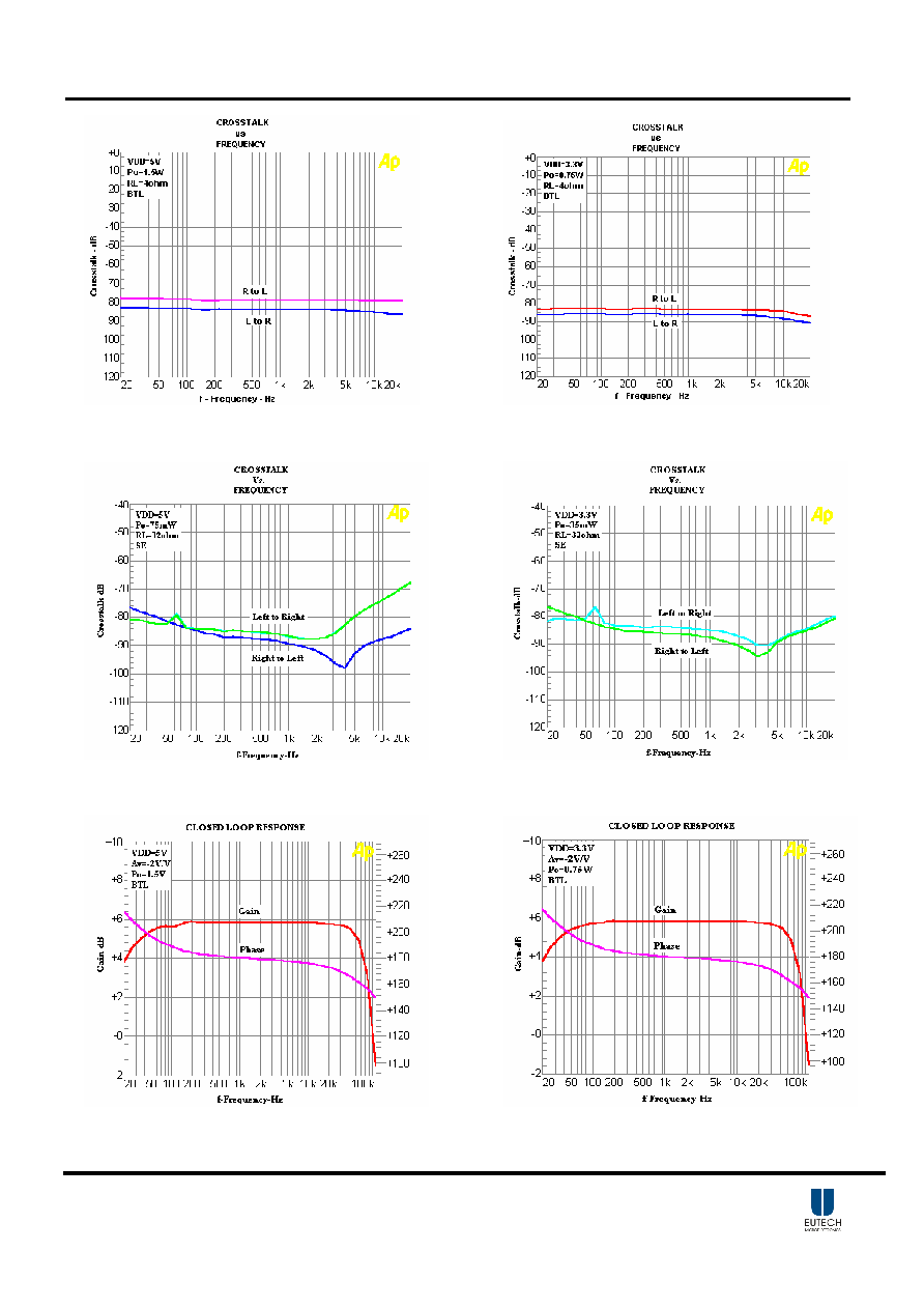
Crosstalk vs .Frequency
VDD=5VPo=1.5WRL=4 ohmBTLRight to Left & Left to Right
39
15
38
Crosstalk vs .Frequency
VDD=3.3VPo=0.75WRL=4 ohmBTLRight to Left & Left to Right
40
15
39
Crosstalk vs .Frequency
VDD=5VPo=75mWRL=32 ohmSERight to Left & Left to Right
41
15
40
Crosstalk vs .Frequency
VDD=3.3VPo=35mWRL=32 ohmSERight to Left & Left to Right
42
15
41
Closed Loop Response
VDD=5VAv=-2V/VPo=1.5WBTLGain & Phase
43
15
42
Closed Loop Response
VDD=3.3VAv= -2V/VPo=0.75WBTLGain &Phase
44
15
43
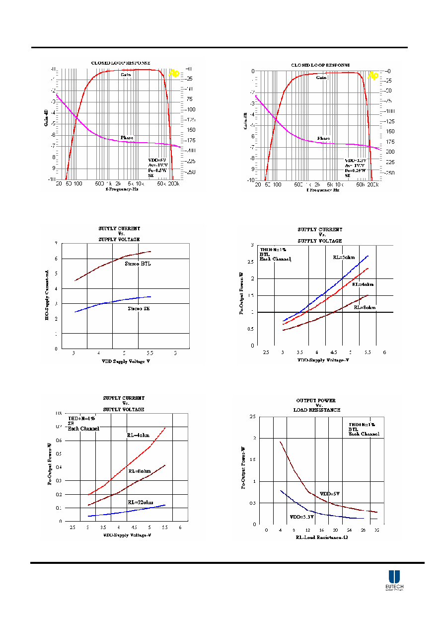
Closed Loop Response
VDD=5VAv=-1V/VPo=0.5WSEGain &Phase
45
16
44
Closed Loop Response
VDD=3.3VAv= -1V/VPo=0.25WSEGain &Phase
46
16
45
Supply Current vs. Supply Voltage Stereo BTL & Stereo SE
47
16
46
Output Power vs. Supply Voltage
THD+N=1
%
BTLEach ChannelRL=3 & 4 & 8 ohm
48
16
47
Output Power vs. Supply Voltage
THD+N=1
%
SEEach ChannelRL=3 & 4 & 8 ohm
49
16
48
Output Power vs. Load Resistance THD+N=1
%
BTLEach ChannelVDD=3.3 & 5V
50
16
49
Output Power vs. Load Resistance THD+N=1
%
SEEach ChannelVDD=3.3 & 5V
51
17
50
Power Dissipation vs. Output Power VDD=5VBTLEach ChannelRL=3 & 4 & 8ohm
52
17
51
Power Dissipation vs. Output Power VDD=3.3VBTLEach ChannelRL=3 & 4 & 8ohm
53
17
52
Power Dissipation vs. Output Power VDD=5VSEEach ChannelRL=4 & 8 &32 ohm
54
17
53
Power Dissipation vs. Output Power VDD=3.3VSEEach ChannelRL=4 & 8 &32 ohm
55
17
EUA5202
DS5202 Ver 1.4 Nov. 2004
9
Figure 3. Figure 4.
Figure5. Figure6.
Figure7. Figure8.
EUA5202
DS5202 Ver 1.4 Nov. 2004
10
Figure9. Figure10.
Figure11. Figure12.
Figure13. Figure14.
EUA5202
DS5202 Ver 1.4 Nov. 2004
11
Figure15. Figure16.
Figure17. Figure18.
Figure19. Figure20.
EUA5202
DS5202 Ver 1.4 Nov. 2004
12
Figure21. Figure22.
Figure23. Figure24.
Figure25.
Figure26.
EUA5202
DS5202 Ver 1.4 Nov. 2004
13
Figure27.
Figure28.
Figure29. Figure30.
Figure31. Figure32.
EUA5202
DS5202 Ver 1.4 Nov. 2004
14
Figure33. Figure34.
Figure35. Figure36.
Figure37. Figure38.
EUA5202
DS5202 Ver 1.4 Nov. 2004
15
Figure39. Figure40.
Figure41. Figure42.
Figure43. Figure44.
EUA5202
DS5202 Ver 1.4 Nov. 2004
16
Figure45. Figure46.
Figure47. Figure48.
Figure49. Figure50.
EUA5202
DS5202 Ver 1.4 Nov. 2004
17
Figure51. Figure52.
Figure53. Figure54.
Figure55.
EUA5202
DS5202 Ver 1.4 Nov. 2004
18
Application Information
Gain Setting Resistors, R
F
and R
I
The gain for each audio input of the EUA5202 is set by
resistors by resistors R
F
and R
I
according to equation 1
for BTL mode.
--------------------------------
(1)
BTL mode operation brings about the factor 2 in the gain
equation due to the inverting amplifier mirroring the
voltage swing across the load. Given that the EUA5202
is a MOS amplifier, the input impedance is very high,
value of R
F
increases. In addition, a certain range of R
F
values is required for proper start-up operation of the
amplifier. Taken together it is recommended that the
effective impedance seen by the inverting node of the
amplifier
be
set
between 5k and 20k .The effective
impedance is calculated in equation 2.
--------------------
(2)
As an example consider an input resistance of 10k and
a feedback resistor of 50k. The BTL gain of the
amplifier would be -10 and the effective impedance at
the inverting terminal would be 8.3k, which is well
within the recommended range. For high performance
applications metal film resistors are recommended
because they tent to have lower noise levels than carbon
resistors. For
values
of
R
F
above 50k
the amplifier
tends to become unstable due to a pole formed from R
F
and the inherent input capacitance of the MOS input
structure. For this reason, a small compensation
capacitor of approximately 5pF should be places in
parallel with R
F
when R
F
is greater than 50k. This, in
effect, creates a low pass filter network with the cutoff
frequency defined in equation 3.
-------------------- (3)
For example, if
R
F
is 100k and C
F
is 5 pF then
f
C
is 318
KHz, which is well outside of the audio range.
Input Capacitor, C
I
In the typical application an input capacitor, C
I
, is
required to allow the amplifier to bias the input signal to
the proper dc level for optimum operation. In this case,
C
I
and R
I
form a high-pass filter with the corner
frequency determined in equation 4.
------------------- (4)
The value
of
C
I
is important to consider as it directly
affects the bass (low frequency) performance of the
circuit. Consider the example where R
I
is 10k and the
specification calls for a flat bass response down to 40Hz.
Equation 8 is reconfigured as equation 5.
------------------------------------ (5)
In this example, C
I
is 0.40 µF so one would likely
choose a value in the range of 0.47µF to 1µF. A further
consideration for this capacitor is the leakage path from
the input source through the input network (R
I
, C
I
) and
the feedback resistor (R
F
) to the load. This leakage
current creates a dc offset voltage at the input to the
amplifier that reduces useful headroom, especially in
high gain applications. For this reason a low-leakage
tantalum or ceramic capacitor is the best choice. When
polarized capacitors are used, the positive side of the
capacitor should face the amplifier input in most
applications as the dc level there is held at V
DD
/2, which
is likely higher that the source dc level. Please note that
it is important to confirm the capacitor polarity in the
application.
C
f
I
R
2
1
I
C
=
-
=
I
R
F
R
2
Gain
BTL
I
F
I
F
R
R
R
R
mpedance
EffectiveI
+
=
I
C
I
R
2
1
)
c(highpass
f
=
F
C
F
R
2
1
(lowpass)
c
f
=
EUA5202
DS5202 Ver 1.4 Nov. 2004
19
Power Supply Decoupling, C
S
The EUA5202 is a high-performance CMOS audio
amplifier that requires adequate power supply
decoupling to ensure the output total harmonic distortion
(THD) is as low as possible. Power supply decoupling
also prevents oscillations for long lead lengths between
the amplifier and the speaker. The optimum decoupling
is achieved by using two capacitors of different types of
noise on the power supply leads. For higher frequency
transients, spikes, or digital hash on the line, a good low
equivalent series - resistance (ESR) ceramic capacitor,
typically 0.1µF placed as close as possible to the device
V
DD
lead works best. For filtering lower frequency
noise signals, a larger aluminum electrolytic capacitor of
10 µF or greater placed near the audio power amplifier is
recommended.
Bypass Capacitor, C
B
The bypass capacitor, C
B
, is the most critical capacitor
and serves several important functions. During startup or
recovery from shutdown mode, C
B
determines the rate at
which the amplifier starts up. The second function is to
reduce noise produced by the power supply caused by
coupling into the output drive signal. This noise is from
the midrail generation circuit internal to the amplifier,
which appears as degraded PSRR and THD+N. Bypass
capacitor, C
B
, values of 0.1 µF to 1 µF ceramic of
tantalum low-ESR capacitors are recommended for the
best THD and noise performance.
In Figure 2, the full feature configuration, two bypass
capacitors are used. This provides the maximum
separation between right and left drive circuits.When
absolute minimum cost and/or component space is
required, one bypass capacitor can be used as shown in
Figure 1. It is critical that terminals 6 and 19 be tied
together in this configuration.
Output Coupling Capacitor, C
C
In the typical single-supply SE configuration, and output
coupling capacitor (C
C
) is required to block the dc bias
at the output of the amplifier thus preventing dc currents
in the load. As with the input coupling capacitor and
impedance of the load form a high-pass filter governed
by equation 6
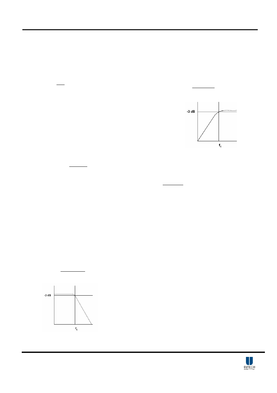
fc(high)= ---------------------------- (6)
The main disadvantage, from a performance standpoint,
is the load impedances are typically small, which drives
the low-frequency corner higher degrading the bass
response. Large values of
C
C
are required to pass low
frequencies into the load. Consider the example where a
C
C
of 330 µF is chosen and loads vary from 3, 4, 8,
32, 10k, to 47k. Table 1 summarizes the frequency
response characteristics of each configuration.
Table1. Common Load Impedances vs Low Frequency Output
Characteristics in SE Mode
R
L
C
C
Lowest Frequency
3
330 µF
161 Hz
4
330 µF
120 Hz
8
330 µF
60 Hz
32
330 µF
15 Hz
10000
330 µF
0.05 Hz
47000
330 µF
0.01 Hz
As Table 1 indicates, most of the bass response is
attenuated into 4 load, an 8 load is adequate,
headphone response is good, and drive into line level
inputs (a home stereo for example) is exceptional.
Using Low-ESR Capacitors
Low-ESR capacitors are recommended throughout this
applications section. A real (as opposed to ideal)
capacitor can be modeled simply as a resistor in series
with an ideal capacitor. The voltage drop across this
resistor minimizes the beneficial effects of the capacitor
in the circuit. The lower the equivalent value of this
resistance
the more the real capacitor behaves like an
ideal capacitor.
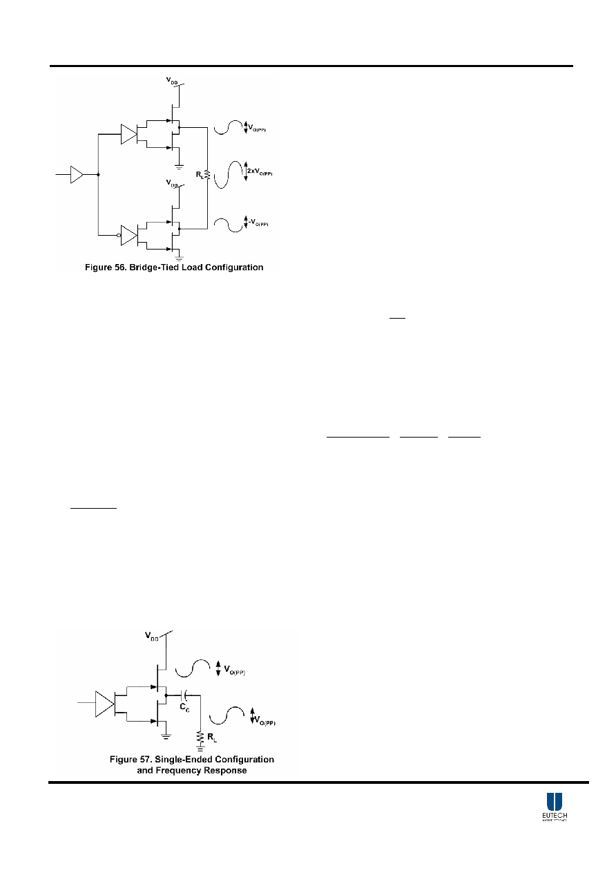
Bridged-tied Load Versus Single-ended Mode
Figure 56 show a linear audio power amplifier (APA) in
a BTL configuration. The EUA 5202 BTL amplifier
consists of two linear amplifiers driving both ends of the
load. There are several potential benefits to this
differential drive configuration, but initially consider
power to the load. The differential drive to the speaker
means that as one side is slewing up, the other side is
slewing down, and vice versa. This in effect doubles the
voltage swing on the load as compared to a ground
referenced load. Plugging 2
×
V
O(PP)
into the power
equation, where voltage is squared, yields 4 × the output
power from the same supply rail and load impedance
(see equation 7 )
V
(rms)
Power ------ (7)
2
2
O(PP)
V
L
R
2
(rms)
V
C
C
R
2
1
L
EUA5202
DS5202 Ver 1.4 Nov. 2004
20
In a typical computer sound channel operating at 5V,
bridging raises the power into
an
8- speaker from a
singled -ended (SE, ground reference) limit of 250 mW
to 1W. In sound power that is a 6-dB improvement--
which is loudness that can be heard. In addition to
increased power there are frequency response concerns.
Consider the single-supply SE configuration shown in
Figure 57. A coupling capacitor is required to block the
dc offset voltage from reaching the load. These
capacitors can be quite large (approximately 33µF to
1000µF) so they tend to be expensive, heavy, occupy
valuable PCB area, and have the additional drawback of
limiting low-frequency performance of the system.
This frequency limiting effect is due to the high pass
filter network created with the speaker impedance and
the coupling capacitance
and is calculated with equation
8.
f
C
=
C
L
C
R
2
1
------------------------------------
(8)
For example,
a 68µF capacitor with
an 8- speaker
would attenuate low frequencies below 293 Hz. The
BTL configuration cancels the dc offsets, which
eliminates the need for the blocking capacitors.
Low-frequency performance is then limited only by the
input network and speaker response. Cost and PCB
space are also minimized by eliminating the bulky
coupling capacitor.
Increasing power to the load does carry a penalty of
increased internal power dissipation. The increased
dissipation is understandable considering that the BTL
configuration produces 4 × the output power of the SE
configuration. Internal dissipation versus output power is
discussed further in the crest factor and thermal
considerations section.
S
ingle-Ended Operation
In SE mode (see Figure56 and Figure57), the load is
driven from the primary amplifier output for each
channel (OUT+, terminals 22 and 3).
In SE mode the gain is set by the R
F
and R
I
resistors and
is shown in equation 9. Since the inverting amplifier is
not used to mirror the voltage swing on the load, the
factor of 2, from equation 5, is not included.
SE Gain =
-
I
R
F
R
-------------------------------------- (9)
The output coupling capacitor required in single-supply
SE mode also places additional constraints on the
selection of other components in the amplifier circuit.
The rules described earlier still hold with the addition of
the following relationship (see equation 10):
C
C
L
R
1
I
R
I
C
1
k
25
B
C
1
<
×
--------------- (10)
EUA5202
DS5202 Ver 1.4 Nov. 2004
21
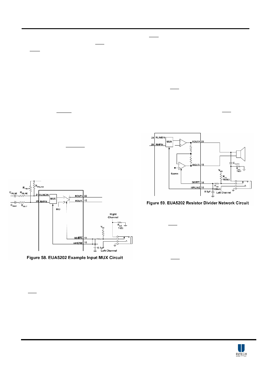
Input MUX operation
Working in concert with the
BTL
SE/
feature, the
LINE
HP/
MUX feature gives the audio designer the
flexibility of a multichip design in a single IC (see
Figure 58). The primary function of the MUX is to allow
different gain settings for BTL versus SE mode.
Speakers typically require approximately a factor of 10
more gain for similar volume listening levels as
compared to headphones. To achieve headphone and
speaker listening parity, the resistor values would need
to be set as follows:
-------------------------- (11)
If, for example R
I (HP)
= 10 k and R
F (HP)
= 10k then
SE Gain
(HP)
= -1
-
=
(LINE)
I
(LINE)
F
(LINE)
R
R
2
Gain
BTL
-------------------- (12)
If, for example
R
I (LINE)
= 10k and R
F (LINE)
= 50k then
BTL Gain
(LINE)
= -10
Another advantage of using the MUX feature is setting
the gain of the headphone channel to -1. This provides
the optimum distortion performance into the headphones
where clear sound is more important. Refer to the
BTL
SE/
operation section for a description of the
headphone hack control circuit.
BTL
SE/
Operation
The ability of the EUA5202 to easily switch between
BTL and SE modes is one of its most important cost
saving features. This feature eliminates the requirement
for an additional headphone amplifier in applications
where internal stereo speakers are driven in BTL mode
but external headphone or speakers must be
accommodated. Internal to the EUA5202, two separate
amplifiers drive LOUT- and ROUT- (terminals 10 and
15).When
BTL
SE/
is held high, the OUT- amplifier
are in high output impedance state, which configures the
EUA5202 as an SE driver from LOUT + and ROUT +
(terminal 3 and 22). I
DD
is reduced by approximately
one-half in SE mode. Control of the
BTL
SE/
input can
be from a logic-level CMOS source, or, more typically,
from a resistor divider network as shown in Figure 59.
Using a readily available 1/8-in. (3.5mm) stereo
headphone jack, the control switch is closed when no
plug is inserted. When closed the 100-k
/
1-k divider
pulls the
BTL
SE/
input low. When a plug is inserted,
the OUT- amplifier is shutdown causing the speaker to
mute (virtually open-circuits the speaker). The OUT+
amplifier then drives through the output capacitor (CO)
into the headphone jack. As shown n the full feature
application (Figure 2), the input MUX control can be
tied to the
BTL
SE/
input. The benefits of doing this are
described in the following input MUX operation section.
Mute and Shutdown Mode
The EUA5202 employs both a mute and a shutdown
mode of operation designed to reduce supply current, I
DD
,
to the
absolute minimum level during periods of nonuse
for battery-power conservation. The SHUTDOWN input
terminal should be held low during normal operation
when the amplifier is in use. Pulling SHUTDOWN high
causes the outputs to mute and the amplifier to enter a
low-current state, I
DD
= 5 µA. SHUTDOWN or MUTE
IN should never be left unconnected because amplifier
operation would be unpredictable. Mute mode alone
reduces I
DD
to 1.5 mA.
-
=
(HP)
I
(HP)
F
(HP)
R
R
Gain
SE
EUA5202
DS5202 Ver 1.4 Nov. 2004
22
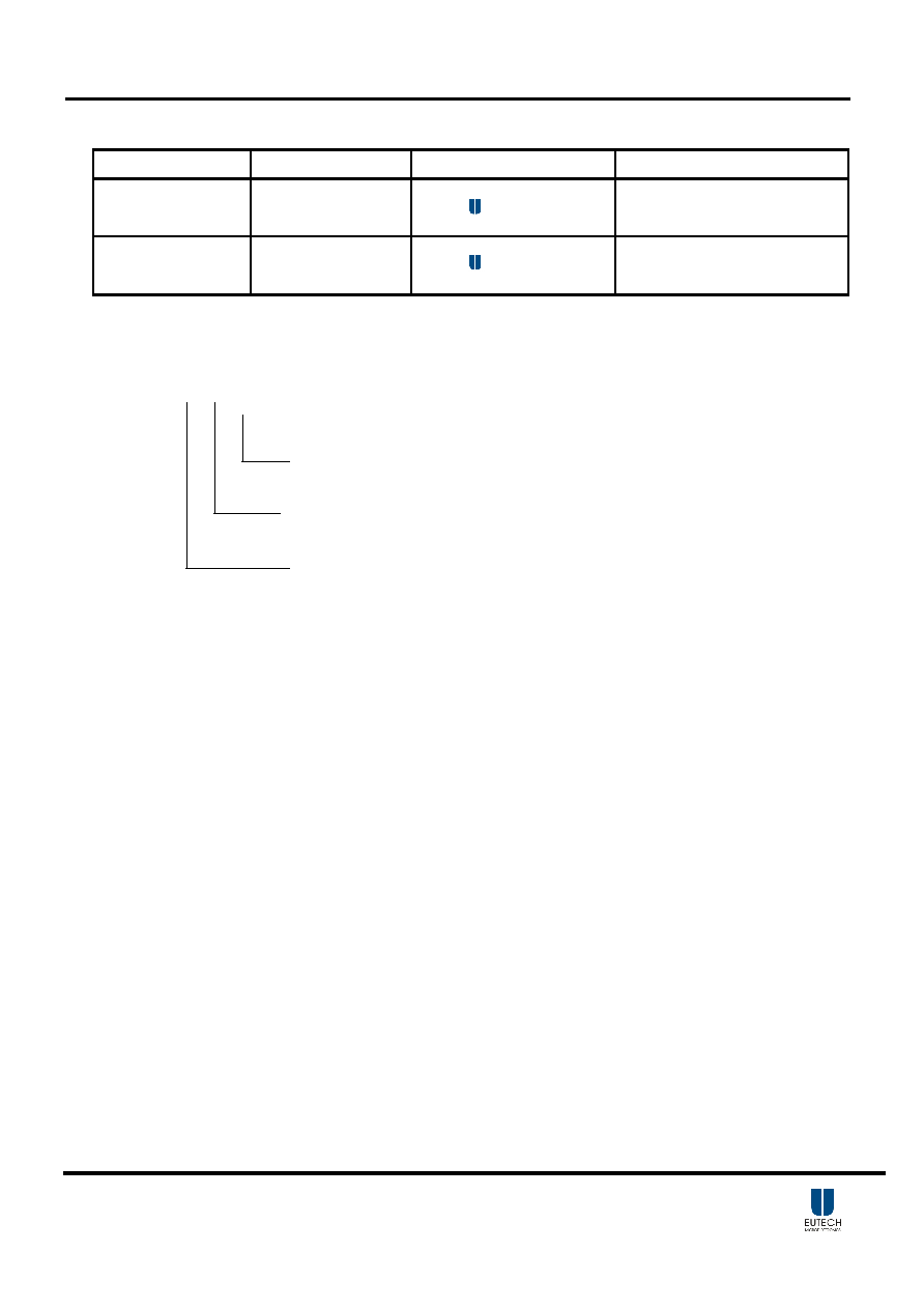
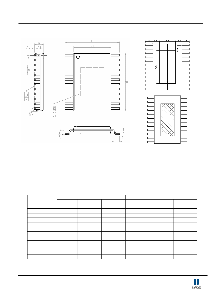
Package Information
NOTE
1. Package body sizes exclude mold flash protrusions or gate burrs
2. Tolerance
±
0.1mm unless otherwise specified
3. Coplanarity :0.1mm
4. Controlling dimension is millimeter. Converted inch dimensions are not necessarily exact.
5. Die pad exposure size is according to lead frame design.
6. Standard Solder Map dimension is millimeter.
7. Followed from JEDEC MO-153
DIMENSIONS IN MILLIMETERS
DIMENSIONS IN INCHES
SYMBOLS
MIN. NOM. MAX. MIN. NOM. MAX.
A ------
------
1.15
------
------
0.045
A1 0.00 ------ 0.10 0.000 ------ 0.004
A2 0.80 1.00 1.05 0.031 0.039 0.041
b
0.19 ------ 0.30 0.007 ------ 0.012
C
0.09 ------ 0.20 0.004 ------ 0.008
D 7.70
7.80
7.90
0.303
0.307
0.311
E
------ 6.40 ----- ------ 0.252 ------
E1
4.30 4.40 4.50 0.169 0.173 0.177
e
------ 0.65 ----- ------ 0.026 ------
L
0.45 0.60 0.75 0.018 0.024 0.030
y ------
------
0.10
------
------
0.004
0 ------ 8 0 ------ 8
Use as much
copper area
as possible
Bottom view
Exposed Pad