
Datasheet
BSP-15 Processor
Datasheet
Equator Technologies, Inc.
Revision H
September 6, 2002
Document Number: HWR.BSP15.DS.REV.H

Datasheet
BSP-15 Processor Datasheet
Revision H
September 6, 2002
Copyright � 2002 Equator Technologies, Inc.
All rights reserved.
Equator makes no warranty for the use of its products, assumes no responsibility for any errors
which may appear in this document, and makes no commitment to update the information
contained herein. Equator reserves the right to change or discontinue this product at any time,
without notice. There are no express or implied licenses granted hereunder to design or
fabricate any integrated circuits based on information in this document.
The following are trademarks of Equator Technologies, Inc., and may be used to identify
Equator products only: Equator, the Equator logo, Equator Around, the Equator Around logo,
MAP, MAP1000, MAP1000A, MAP-CA, MAP Series, Broadband Signal Processor, BSP,
FIRtree, DataStreamer, DS, iMMediaC, iMMediaTools, iMMediaToolsLite, Media Intrinsics,
VersaPort, SofTV, StingRay, Dolphin, Tetra, and Barracuda. Other product and company
names contained herein may be trademarks of their respective owners.
The MAP-CA digital signal processor was jointly developed by Equator Technologies, Inc.,
and Hitachi, Ltd.
Versions of this document released prior to 01-Apr-2002 are:
Copyright � 2000 - 2001 Equator Technologies, Inc., and Hitachi, Ltd.
All rights reserved.

September 6, 2002
HWR.BSP15.DS.REV.H
BSP-15 Processor Datasheet
iii
Table of Contents
Preface
...................................................................................................................... xi
Type style conventions ............................................................................................................... xi
Chapter 1
Introduction
.............................................................................................................. 1
1.1
Overview .................................................................................................................................... 1
1.1.1
Features...............................................................................................................................
1
1.1.2
Related Documents.............................................................................................................
3
Chapter 2
Architecture Overview
.......................................................................................... 5
2.1
The VLIW Core ......................................................................................................................... 6
2.1.1
Execution Units ..................................................................................................................
6
2.1.1.1
I-ALU..................................................................................................................... 7
2.1.1.2
IG-ALU .................................................................................................................. 7
2.1.1.3
Simple Interlocks ................................................................................................... 7
2.1.1.4
Extensive Predication............................................................................................. 7
2.1.2
Register Resources .............................................................................................................
7
2.1.2.1
Global Registers ..................................................................................................... 8
2.1.2.2
Breakpoint Registers .............................................................................................. 8
2.1.2.3
General Registers ................................................................................................... 8
2.1.2.4
Predicate Registers ................................................................................................. 8
2.1.2.5
PLC/PLV 128-bit registers..................................................................................... 8
2.2
Interrupts and Exceptions........................................................................................................... 8
2.2.1
Core Interrupts and Exceptions ..........................................................................................
9
2.2.2
Interrupt Controller.............................................................................................................
9
2.3
Timers....................................................................................................................................... 10
2.4
Memory Hierarchy ................................................................................................................... 10
2.4.1
Caches...............................................................................................................................
11
2.4.2
Address Translation..........................................................................................................
11
2.5
Databuses and Controllers........................................................................................................ 11
2.5.1
Memory Interface Controller............................................................................................
11
2.5.2
Data Transfer Switch (DTS).............................................................................................
12
2.5.3
DataStreamer DMA Controller ........................................................................................
12
2.5.4
PCI Bus.............................................................................................................................
12
2.5.5
I/O Bus..............................................................................................................................
13
2.6
Coprocessors ............................................................................................................................ 13
2.6.1
VLx...................................................................................................................................
13
2.6.2
Video Filter.......................................................................................................................
13
2.6.3
DES Module .....................................................................................................................
13
2.7
I/O Interfaces............................................................................................................................ 14

iv
BSP-15 Processor Datasheet
HWR.BSP15.DS.REV.H
September 6, 2002
2.7.1
Audio Interfaces ...............................................................................................................
14
2.7.1.1
IEC958 Audio Interface ....................................................................................... 14
2.7.1.2
IIS Interface.......................................................................................................... 14
2.7.2
Video Interfaces................................................................................................................
14
2.7.2.1
Transport Channel Interfaces ............................................................................... 14
2.7.2.2
ITU-656 Input Interface ....................................................................................... 15
2.7.2.3
ITU-656 Output Interface .................................................................................... 15
2.7.2.4
General Purpose Data Port (GPDP) ..................................................................... 15
2.7.3
Display Refresh Controller...............................................................................................
15
2.7.4
Analog RGB .....................................................................................................................
15
2.7.5
Digital RGB......................................................................................................................
16
2.7.6
IIC Interface Unit .............................................................................................................
16
2.7.7
ROM Controller................................................................................................................
16
2.7.8
Reset Strap........................................................................................................................
17
Chapter 3
BGA Pin-out Assignments
................................................................................. 19
Chapter 4
Signal Descriptions
............................................................................................... 25
4.1
Interface Summary ................................................................................................................... 25
4.2
Legend ...................................................................................................................................... 26
4.3
Processor Clock........................................................................................................................ 26
4.4
SDRAM.................................................................................................................................... 27
4.5
PCI Bus .................................................................................................................................... 27
4.6
IEC958 ..................................................................................................................................... 29
4.7
IIS ............................................................................................................................................. 29
4.8
Multi-Function Signal Pins ...................................................................................................... 30
4.8.1
Transport Channel Interfaces (TCI) .................................................................................
31
4.8.2
ITU-656 Inputs .................................................................................................................
32
4.8.3
ITU-656 Output ................................................................................................................
33
4.8.4
General Purpose Data Port (GPDP) .................................................................................
33
4.8.5
Flash ROM .......................................................................................................................
34
4.8.6
Reset Straps ......................................................................................................................
34
4.9
Analog CRT ............................................................................................................................. 35
4.10
Digital RGB............................................................................................................................ 35
4.11
IIC........................................................................................................................................... 36
4.12
Boundary Scan (JTAG) .......................................................................................................... 36
4.13
Power/Ground Pins ................................................................................................................ 37
4.14
Signal List Summary .............................................................................................................. 37
Chapter 5
External Connection Examples
......................................................................... 39
5.1
SDRAM ................................................................................................................................... 39
5.2
IEC958 ..................................................................................................................................... 42
5.3
IIS ............................................................................................................................................. 42
5.4
Transport Channel Interface (TCI)........................................................................................... 43
5.5
NTSC Decoder ......................................................................................................................... 43

v
September 6, 2002
HWR.BSP15.DS.REV.H
BSP-15 Processor Datasheet
5.6
NTSC Encoder ......................................................................................................................... 44
5.7
CRT .......................................................................................................................................... 44
5.8
IIC............................................................................................................................................. 45
5.9
ROM......................................................................................................................................... 45
Chapter 6
Electrical Specifications
...................................................................................... 47
6.1
Absolute Maximum Ratings..................................................................................................... 47
6.2
Power Supply Specifications.................................................................................................... 48
6.3
BSP-15 DC Characteristics ...................................................................................................... 49
6.4
AC Characteristics.................................................................................................................... 50
6.4.1
PLL reference clock input ................................................................................................
50
6.4.2
SDRAM interface timing .................................................................................................
50
6.4.3
PCI bus timing ..................................................................................................................
52
6.4.4
IEC958 interface timing ...................................................................................................
54
6.4.5
IIS interface timing...........................................................................................................
54
6.4.6
Transport Channel Interface timing..................................................................................
58
6.4.7
ITU-R BT.601/656 interface timing.................................................................................
59
6.4.8
General Purpose Data Port ...............................................................................................
60
6.4.9
IIC interface timing ..........................................................................................................
61
6.4.10
dRGB timing ..................................................................................................................
62
6.5
Termination Characteristics ..................................................................................................... 63
6.5.1
Basic rules ........................................................................................................................
63
6.5.1.1
Weak pull down and pull up defined ................................................................... 63
6.5.2
Processor clock .................................................................................................................
64
6.5.3
ROMCON.........................................................................................................................
64
6.5.4
PCI ....................................................................................................................................
65
6.5.5
ITU-R BT.601/656 out .....................................................................................................
66
6.5.6
Video input ports ..............................................................................................................
66
6.5.6.1
TCIA .................................................................................................................... 66
6.5.6.2
TCIB..................................................................................................................... 67
6.5.7
ITU-R BT.601/656 IN_A .................................................................................................
67
6.5.8
ITU-R BT.601/656 IN_B .................................................................................................
67
6.5.9
IIS .....................................................................................................................................
67
6.5.10
IEC958............................................................................................................................
68
6.5.11
IIC/DDC .........................................................................................................................
68
6.5.12
JTAG ..............................................................................................................................
68
6.5.13
DRC / VideoDAC...........................................................................................................
68
Chapter 7
Thermal Specifications
........................................................................................ 71
Chapter 8
Mechanical Specifications
.................................................................................. 73
8.1
EBGA352 Package................................................................................................................... 73
8.2
Package Materials .................................................................................................................... 74
8.2.1
Materials specification......................................................................................................
74
8.2.2
Index Location..................................................................................................................
74

vi
BSP-15 Processor Datasheet
HWR.BSP15.DS.REV.H
September 6, 2002
Appendix A
Glossary
.............................................................................................................. 75

September 6, 2002
HWR.BSP15.DS.REV.H
BSP-15 Processor Datasheet
vii
List of Tables
Table 2-1
Events That Can Trigger Interrupts ......................................................................... 9
Table 2-2
Supported Interrupts .............................................................................................. 10
Table 3-1
Pin Assignments .................................................................................................... 19
Table 4-1
Processor clock signal description......................................................................... 26
Table 4-2
Memory interface signals ...................................................................................... 27
Table 4-3
PCI interface signals .............................................................................................. 27
Table 4-4
IEC958 interface signals........................................................................................ 29
Table 4-5
IIS interface signals ............................................................................................... 29
Table 4-6
Multiple Signal Pins .............................................................................................. 30
Table 4-7
Primary TCI Interface Signals ............................................................................... 31
Table 4-8
Secondary TCI Interface Signals ........................................................................... 32
Table 4-9
Primary ITU-R BT.601/656 Input Interface Signals ............................................. 32
Table 4-10
Secondary ITU-R BT.601/656 Input Interface Signals ......................................... 33
Table 4-11
ITU-R BT.601/656 Output Interface Signals ........................................................ 33
Table 4-12
GPDP Interface Signals ......................................................................................... 33
Table 4-13
ROM Interface Signals .......................................................................................... 34
Table 4-14
Reset Straps ........................................................................................................... 34
Table 4-15
CRT Interface Signals ........................................................................................... 35
Table 4-16:
Digital RGB interface signals................................................................................ 35
Table 4-17
IIC Interface Signals .............................................................................................. 36
Table 4-18
JTAG Interface Signals ......................................................................................... 36
Table 4-19
Power/Ground Pins................................................................................................ 37
Table 4-20
BSP-15 DSP Pin List ............................................................................................. 37
Table 6-1
Absolute Maximum Ratings .................................................................................. 47
Table 6-2
Voltage Variation .................................................................................................. 48
Table 6-3
Steady State Current .............................................................................................. 48
Table 6-4
Input/Output Signals.............................................................................................. 49
Table 6-5
Video DAC outputs - aRGB mode ........................................................................ 49
Table 6-6
PLL Reference Clock Input Conditions ................................................................ 50
Table 6-7
SDRAM interface timing parameters .................................................................... 51
Table 6-8
PCI interface timing parameters ............................................................................ 53
Table 6-9
PCI measurement conditions ................................................................................. 53
Table 6-10
IEC958 interface timing parameters...................................................................... 54
Table 6-12
IIS output timing parameters ................................................................................. 55
Table 6-11
IIS clock ratios....................................................................................................... 55

viii
BSP-15 Processor Datasheet
HWR.BSP15.DS.REV.H
September 6, 2002
Table 6-13
IIS input timing parameters - slave mode.............................................................. 56
Table 6-14
IIS input timing parameters - master mode ........................................................... 57
Table 6-15
TCI timing parameters........................................................................................... 58
Table 6-16
ITU-R BT.601/656 input interface timing parameters .......................................... 59
Table 6-17
ITU-R BT.601/656 output interface timing parameters ........................................ 60
Table 6-18
GPDP input timing parameters.............................................................................. 60
Table 6-19
GPDP output timing parameters............................................................................ 61
Table 6-20
IIC interface timing parameters ............................................................................. 62
Table 6-21
Processor Clock Terminations............................................................................... 64
Table 6-22
ROMCOM Terminations....................................................................................... 64
Table 6-23
PCI Termination .................................................................................................... 65
Table 6-24
ITU-R BT.601/656 Out Termination..................................................................... 66
Table 6-25
TCIA Terminations................................................................................................ 66
Table 6-26
TCIA Terminations................................................................................................ 67
Table 6-27
ITU-R BT.601/656 IN_A Terminations ................................................................ 67
Table 6-28
ITU-R BT.601/656 IN_B Terminations ................................................................ 67
Table 6-29
IIS Terminations .................................................................................................... 67
Table 6-30
IEC 958 Terminations ........................................................................................... 68
Table 6-31
IIC/DDC Terminations .......................................................................................... 68
Table 6-32
JTAG Terminations ............................................................................................... 68
Table 6-33
DRC / VideoDAC.................................................................................................. 68
Table 7-1
Thermal Parameters ............................................................................................... 71
Table 8-1
Materials specification........................................................................................... 74

September 6, 2002
HWR.BSP15.DS.REV.H
BSP-15 Processor Datasheet
ix
List of Figures
Figure 1.1
Equator BSP-15 Processor System Diagram............................................................ 2
Figure 2.1
BSP-15 DSP/CPU block diagram............................................................................. 5
Figure 3.1
BSP-15 DSP pins viewed from bottom .................................................................. 22
Figure 3.2
BSP-15 DSP pins viewed from top ........................................................................ 23
Figure 4.1
BSP-15 Interface..................................................................................................... 25
Figure 5.1
64-bit, 4 MB configuration using �32, 8 Mb parts................................................. 39
Figure 5.2
64-bit, 16 MB configuration using �8, 16 Mb parts............................................... 39
Figure 5.3
64-bit, 16 MB configuration using �16 16 Mb parts.............................................. 40
Figure 5.4
64-bit, 64 MB configuration using �16, 64 Mb parts............................................. 40
Figure 5.5
64-bit, 64 MB configuration using �16, 128 Mb parts........................................... 41
Figure 5.6
64-bit, 128 MB configuration using �16, 128 Mb parts......................................... 41
Figure 5.7
IEC958 interface..................................................................................................... 42
Figure 5.8
IIS interface ............................................................................................................ 42
Figure 5.9
Transport Channel Interface ................................................................................... 43
Figure 5.10
ITU-R BT.656 NTSC/PAL decoder interface ........................................................ 43
Figure 5.11
NTSC/PAL encoder interface................................................................................. 44
Figure 5.12
CRT ........................................................................................................................ 44
Figure 5.13
IIC interface ............................................................................................................ 45
Figure 5.14
ROM connections ................................................................................................... 45
Figure 6.1
SDRAM timing measurement conditions............................................................... 50
Figure 6.2
PCI output timing measurement conditions ........................................................... 52
Figure 6.3
PCI input timing measurement conditions ............................................................. 52
Figure 6.4
IIS data format ........................................................................................................ 54
Figure 6.5
IIS output timing measurement conditions............................................................. 55
Figure 6.6
IIS input timing measurement - slave mode ........................................................... 56
Figure 6.7
IIS input timing measurement - master mode ........................................................ 56
Figure 6.8
Internal serial clock generation for IIS master mode ............................................. 57
Figure 6.9
TCI timing measurement conditions ...................................................................... 58
Figure 6.10
ITU-R BT.601/656 input timing measurement conditions..................................... 59
Figure 6.11
ITU-R BT.601/656 output timing measurement conditions................................... 59
Figure 6.12
GPDP input timing measurement conditions ......................................................... 60
Figure 6.13
GPDP output timing measurement conditions ....................................................... 60
Figure 6.14
IIC timing measurement conditions ....................................................................... 61

x
BSP-15 Processor Datasheet
HWR.BSP15.DS.REV.H
September 6, 2002
Figure 6.15
dRGB timing diagram ............................................................................................ 62
Figure 8.1
EBGA352 Package ................................................................................................. 73
Figure 8.2
Index location ......................................................................................................... 74

xi
September 6, 2002
HWR.BSP15.DS.REV.H
BSP-15 Processor Datasheet
Preface
Type style conventions
With the exception of section and subsection headings, the formatting of text in the following doc-
ument adheres to the following conventions:
�
Normal descriptive text is presented in Times New Roman font.
�
Italicized Times New Roman
text is used for document titles.
�
Bold Times New Roman text is used for emphasis in normal descriptive text.
Any input or output text for any computer program is presented in
Courier
New
font. This
includes source code, command-line text, and program output.
Italicized Courier New
text is used for any portion of a path name, including individual
file names.
Bold Courier New
text is used for any placeholder for a set of text input or output items for a
program.

xii
BSP-15 Processor Datasheet
HWR.BSP15.DS.REV.H
September 6, 2002

1
September 6, 2002
HWR.BSP15.DS.REV.H
BSP-15 Processor Datasheet
Chapter 1
Introduction
1.1 Overview
The Equator BSPTM-15 processor is the latest member of the Equator Broadband Signal Processor
family offering highly integrated single chip solutions for broadband products such as set-top
boxes, digital televisions, video conferencing systems, medical imaging products, digital video
editing equipment, and office automation products.
The processing power of the BSP-15 processor combined with iMMediaTools
TM
code generation
environment and library of audio and video codecs provide a proven and effective solution for
building rapidly evolving broadband solutions.
1.1.1 Features
The Equator BSP-15 processor provides the following features:
�
Advanced four-issue, super pipelined Very Long Instruction Word Processor
The VLIW processor provides four integer ALUs, two 64-bit SIMD ALUs, and two 128-bit
SIMD ALUs. The processor has 32 1-bit predicate registers, eight 128-bit registers, and 128
32-bit registers, which can be paired into 64-bit registers.
�
Advanced high throughput memory hierarchy
Instructions are provided to the VLIW processor by a 32 KB two-way set-associative instruc-
tion cache with an LRU replacement policy. Instructions are stored in compressed format. Data
is provided to the processor by a 32 KB four-way set associative, four-bank interleaved data
cache with an LRU replacement policy. Memory protection is provided by separate instruction,
data and DMA MMUs, each with a fully set-associative 16 entry TLB. Off chip memory is con-
nected via a glueless high speed 64-bit SDRAM/SGRAM interface supporting up to 128 MB of
external memory.
�
Specialized coprocessors
Variable length encoding and decoding is handled by the VLx coprocessor with 4 KB instruc-
tion and 4 KB data memory. The Video Filter coprocessor provides up to 4 vertical tap and 5
horizontal tap filtering, aided by a 6 KB line buffer. High data throughput is provided by the
DataStreamerTM, a programmable 64 channel DMA controller with 8 KB of buffering . The
Display Refresh Controller provides color space conversion, palette table lookup and hardware
cursor functionality. A DES coprocessor accelerates DES encryption and decryption.
2
BSP-15 Processor Datasheet
HWR.BSP15.DS.REV.H
September 6, 2002
.
�
I/O interfaces
A large number of interfaces is available, as shown in
Figure 1.1
.
-
33/66 MHz 32-bit PCI interface
-
64-bit SDRAM/SGRAM interface
-
2 DVB compliant transport channel interfaces
1
-
2 ITU 656 inputs
1
-
1 ITU 656 output
1
-
8-bit general purpose data input port (GPDP)
1
-
8-bit general purpose data output port (GPDP)
1
-
Analog RGB interface
-
Digital RGB flat panel interface
1
-
Flash EEPROM interface
1
-
IIC master/slave interface
-
IIS interface
1
1. Interface shares pins with other interface(s)
PCI
SDRAM
TCI A
1
TCI B
1
ITU-656 IN A
1
ITU-656 IN B
1
ITU-656 OUT
1
GPDP IN
GPDP OUT
IEC968
IIS
1
IIC
JTAG
Flash EEPROM
1
Digital RGB
1
Analog RGB
BSP
TM
-15
Processor
Equator
Figure 1.1 Equator BSP-15 Processor System Diagram

3
September 6, 2002
HWR.BSP15.DS.REV.H
BSP-15 Processor Datasheet
-
IEC958 interface
1
-
JTAG interface
Not all interfaces can be active at the same time because of pin multiplexing:
�
TCI A, ITU-656 IN A, GPDP IN, and digital RGB 12/18/24 bit modes share pins and cannot be
used at the same time
�
TCI B, ITU-656 IN B (601 mode) and digital RGB 18/24 bit mode share pins and cannot be
used at the same time
�
IIS and Flash EEPROM interface share pins and cannot be used at the same time
2
�
GPDP OUT, Flash EEPROM and digital RGB 12/18/24 bit modes share pins and cannot be
used at the same time
�
TCI A and B share pins with digital RGB 12/18/24 bit modes share pins and neither one can be
used together with digital RGB.
1.1.2 Related Documents
Equator Hardware Reference, Volume 1: BSP-15 Instruction set, HWR.BSP15.V1
Equator Hardware Reference, Volume 2: BSP-15 VLx and Video Filter, HWR.BSP15.V2
Equator Hardware Reference, Volume 3: BSP-15 Data Controllers, HWR.BSP15.V3
Equator Hardware Reference, Volume 4: BSP-15 I/O Interfaces, HWR.BSP15.V4
Equator Hardware Reference, Volume 5: BSP-15 PIO & Register Maps, HWR.BSP15.V5
1. Interface shares pins with other interface(s)
2. A special IIS bypass mode provides single channel IIS via a TCI IN A pin

4
BSP-15 Processor Datasheet
HWR.BSP15.DS.REV.H
September 6, 2002
September 6, 2002
HWR.BSP15.DS.REV.H
BSP-15 Processor Datasheet
5
Chapter 2
Architecture Overview
The BSP-15 family of digital signal processors are high-performance processors providing broadband
applications with solutions addressing the convergence of communications, consumer appliances and
general purpose computing. The BSP-15 DSP family of chips combines general-purpose RISC-like data
processing with high-performance signal and image processing. The BSP-15 DSP family supports
C-like programmable video, image, and signal processing software implementations of compression
and decompression algorithms. The BSP-15 DSP family matches the cost and performance features of
dedicated fixed-function chips, with the added flexibility to rapidly respond to evolving standards.
Figure 2.1
shows a block diagram of the typical BSP-15 DSP. The BSP-15 DSP consists of a VLIW
core, programmable coprocessors, on-chip memories and I/O interfaces.
The main VLIW core executes four operations in parallel and supports partitioned SIMD operations for
8-, 16-, 32-, and 64-bit data types. Coprocessors on the BSP-15 DSP help accelerate serial operations
like variable length encoding/decoding and video filtering.
Several audio/video I/O interfaces are supported, including ITU-R BT.601/656 input and output; dual
MPEG-2 transport channel interface (TCI); IEC958 and IIS digital audio interfaces. Two video 656
inputs can be used at the same time. The Display Refresh Controller (DRC) supports both analog and
digital RGB outputs. In addition it provides hardware support for graphics/video overlay, hardware
cursor, and color space conversion. An IIC control bus interface is also provided.
32 KB Data
Cach
e
Glueless
SDRAM
Controller
ITU-
656
IN
GPDP
IN
ITU-
656
IN
Video In B
Video In A
GPD
P
Video Out
IE
C95
8
II
S
Audio I/O
IIC
IIC
Display
Refresh
Controller
32-bit IOB
Analog RGB
SDRAM
TCI
IN
TCI
IN
PLLs
27 MHz
Video Filter
6 KB VF
Memory
VLx
8 KB VLx
Memory
ROMCON
JTAG
Boundary Scan
JTAG
Flash
ROM
32-bit
66 MHz
PCI
R
e
gi
st
e
r
Fi
l
e
Re
gi
s
t
e
r
Fi
l
e
I-ALU
IG-ALU
I-ALU
IG-ALU
VLIW Core
3
2
KB In
st
ru
ctio
n
Cach
e
64-bit DTS
DataStreamer DMA
Controller
DES
Figure 2.1 BSP-15 DSP/CPU block diagram
Digital RGB
ITU-
656
OUT

6
BSP-15 Processor Datasheet
HWR.BSP15.DS.REV.H
September 6, 2002
These I/O functions execute in parallel with the CPU and eliminate the need for several external ASICs
with their associated cost and bandwidth issues.
A glueless 64-bit wide SDRAM interface connects the BSP-15 processor to external memory with a
maximum size of 128 MB. The BSP-15 DSP supports a 128 MB maximum memory size. A 32-bit
33/66 MHz PCI bus interface is also supported. The BSP-15 DSP boots from either the PCI bus or the
Flash ROM interface.
There are three on-chip PLLs (core/SDRAM, pixel, audio) that generate all the internal clocks from a
single 27 MHz external clock input (
pclk
). The
tci_vdac
pin can be used to output a controlling
signal that can be used to drive a one bit sigma-delta modulator for an external VCXO which in turns
modulates the frequency on
pclk
.
2.1 The VLIW Core
Real-time processing of multimedia data stresses processor performance, I/O performance and memory
performance. There are three basic ways to increase a processor's performance: decrease the cycle time,
decrease the number of cycles required to execute an instruction, and execute more instructions per
cycle. The first two are becoming increasingly difficult to improve beyond process scheduling, while the
last (executing more instructions per cycle) is now receiving more attention. Executing more
instructions per cycle exploits the natural parallelism available in most software routines. Very Long
Instruction Word (VLIW) processors use this parallelism by packing multiple operations into a single
instruction word, which is then executed as a unit.
VLIW architectures differ from superscalar architectures in that the grouping and scheduling of
instructions for execution is done at compile time, rather than execution time. The compiler searches for
eligible operations, checks for dependencies and resource conflicts, and packages these eligible
operations into VLIW instructions. The VLIW compiler can explore beyond the limited search window
seen in superscalar architectures and cross natural boundaries, such as branches, to search for
opportunities for enhanced parallelism. The Equator compiler uses a technique known as "trace
scheduling" to search a whole routine for eligible operations.
By moving the difficult task of finding parallelism into software, VLIW compiler techniques
dramatically simplify the CPU design by reducing gate count and freeing valuable die area for other
performance enhancements or lower chip costs. While VLIW is primarily designed to exploit
parallelism, its simplification of the processor architecture allows for reduced cycle times as well.
2.1.1 Execution Units
The BSP-15 DSP operations are primarily three-operand RISC operations. As in any typical RISC
architecture, load and store operations are the only means of referencing memory. The BSP-15 DSP has
four functional units: two I-ALUs and two IG-ALUs. Each I-ALU contains a load-store unit, an integer
ALU, and a branch unit. Each IG-ALU contains an integer/graphics unit and a multimedia operation
unit. The I-ALU and IG-ALU support different operations, but many integer and logical operations are
implemented in both units. This overlap allows the compiler to schedule more operations in parallel and
make more efficient use of all the functional units.
There are 128 32-bit registers usable separately or in pairs as 64-bit registers, 32 1-bit predicate
registers, and eight special 128-bit registers for the VLIW core CPU. These 128-bit (PLC/PLV) registers
are used for FIR filter, SAD, FFT, ADD, DCT, and other specialized partitioned integer operations. The
large register files help minimize unnecessary instruction dependencies caused by logically distinct
register reuses.
Each BSP-15 DSP instruction contains four operations per cycle. The Media Intrinsics instructions
include partitioned operations over these media data types. Load and store operations can perform one,
two, four, and eight byte accesses, with support for both little-endian and big-endian byte orderings.

7
September 6, 2002
HWR.BSP15.DS.REV.H
BSP-15 Processor Datasheet
Dynamic address translation and virtual memory protection are fully supported. The 1-bit logical values
are also used to support predicated execution, which substantially enhances available parallelism by
allowing partial speculation and eliminating branching.
2.1.1.1 I-ALU
The I-ALU performs the following operations:
�
32-bit integer arithmetic operations including compare
�
Logical and bitwise logical operations whose results can be sent to general or predicate registers
�
Address calculations for indexed addressing
�
Memory reference
�
Branching
�
System control operations
2.1.1.2 IG-ALU
The IG-ALU performs the following operations:
�
32-bit integer arithmetic operations (same as the I-ALU)
�
Logical and bitwise logical operations (same as the I-ALU)
�
64-bit integer arithmetic operations
�
Shift/extract/merge operations
�
64-bit SIMD operations (with 8-bit, 16-bit, and 32-bit partitions) including selection, comparison,
selection of maximums and minimums, addition, multiply-add, complex multiplication, inner
product, and sum of absolute differences
�
128-bit partitioned (with 8-bit, 16-bit, and 32-bit partitions) SIMD operations including inner-
product with new partition shift-in for efficient FIR operation and sum of absolute differences
with new partition shift-in for efficient block matching operation
2.1.1.3 Simple Interlocks
Certain operations require more than one cycle to complete. No hardware interlocks are needed to
prevent issue of an operation that attempts to read a result not yet completed. The VLIW compiler is
responsible for correct scheduling, not hardware. Register scoreboarding is supported for outstanding
loads.
2.1.1.4 Extensive Predication
Nearly all operations can have their effect controlled by the value of a selected (1-bit) predicate register.
A predicate register is tested to determine whether or not the operation should be performed. This
allows the compiler to aggressively convert control flow into data flow, enabling a substantially higher
degree of instruction-level parallelism. This also greatly helps to reduce any penalties for branching,
without the cost and complexity of hardware branch prediction typical in other General Purpose
processors.
2.1.2 Register Resources
There are several types of registers on the BSP-15 DSP. These include system registers, breakpoint
registers, general purpose registers, predicate registers, and special purpose 128-bit registers.

8
BSP-15 Processor Datasheet
HWR.BSP15.DS.REV.H
September 6, 2002
2.1.2.1 Global Registers
Global registers on the BSP-15 DSP consist of system registers and implementation-dependent I/O
registers (PIO registers). Dedicated operations manipulate the system registers; conventional load and
store operations manipulate the I/O registers.
2.1.2.2 Breakpoint Registers
BSP-15 DSP has two sets of breakpoint registers: instruction-breakpoint and data-breakpoint registers.
These registers provide hardware breakpoint capability for various debugging tools.
Instruction-breakpoint registers cause an exception when an operation in the specified address is about
to be executed. Similarly, the data-breakpoint registers cause an exception when the data at the specified
address is about to be accessed. In both cases, a mask can be used to specify a range of addresses.
By registering an exception handling routine associated with either of these exceptions, a software
developer can control what happens when a hardware breakpoint occurs. For example, the exception
handling routine may be used to signal an external application such as a source-level debugger that a
breakpoint has occurred.
2.1.2.3 General Registers
There are 128 32-bit registers that can be treated as 64-bit general registers using even-odd pairs of the
32-bit registers.
2.1.2.4 Predicate Registers
There are 32 1-bit predicate registers. Predicate registers are used in predicated operations, logical
operations, and branches. They provide a destination for operations with a judged condition.
2.1.2.5 PLC/PLV 128-bit registers
The IG-ALU has eight special 128-bit registers � two pairs of Partitioned Local Constant (PLC)
registers and two pairs of Partitioned Local Variable (PLV) registers. These registers are used for
powerful SIMD DSP partitioned operations. The registers can be configured as sixteen 8-bit operation
partitions, eight 16-bit operation partitions, or four 32-bit operation partitions. For numerous digital
signal processing and compression algorithms, the SIMD operations allows the BSP-15 DSP to match
the cost/performance of fixed-function chips without the loss of re-programmability.
2.2 Interrupts and Exceptions
The BSP-15 DSP has a flexible interrupt structure. Interrupts and exceptions internal to the core are
reflected directly in system registers. All other interrupts from on-chip devices and PCI interrupts from
external devices are gathered by an on-chip interrupt controller. The interrupt controller also provides a
number of software interrupts.
Routing, masking, and prioritization of interrupts is completely software programmable. Each of the
interrupts handled by the interrupt controller can be individually masked, or routed to one of four core
interrupts or to one of two PCI interrupt signals.
9
September 6, 2002
HWR.BSP15.DS.REV.H
BSP-15 Processor Datasheet
2.2.1 Core Interrupts and Exceptions
Table 2-1
lists the events that can trigger interrupts or exceptions within the core. When an event occurs,
a bit is set in an "Event Seen" system register. If the event is not masked (or not maskable), the address
for a handler will be fetched from one of nine Event Vector system registers, depending on the event.
2.2.2 Interrupt Controller
The BSP-15 DSP's interrupt controller supports multiple maskable interrupts from outside of the core.
Non-core interrupt sources include on-chip devices such as TCI, the DRC, the DataStreamer DMA
controller, and PCI interrupts from external devices or hosts. Software-generated shoulder-tap interrupts
are provided for multiprocessing or inter-process communication support.
The BSP-15 DSP interrupts can be examined and controlled via PIO registers in the ROMCON control
block. Routing and masking of interrupts is programmable. Each interrupt can be individually masked
or routed to one of four core interrupts or to one of two PCI interrupt signals. Software interrupts can be
similarly masked and routed. They may be asserted or de-asserted under software control.
Table 2-1 Events That Can Trigger Interrupts
Name
Event
Maskable?
IO0.IO3
I/O interrupts (from interrupt controller)
Yes
SINT0.SINT1
Software interrupts
Yes
FCNT
Free running counter overflow
Yes
INTV0.INTV1
Interval timers
Yes
ILPC
Illegal program counter
No
IBPT
Instruction address break
Yes
BPOP
Breakpoint operation
No
SYS
System call (trap instruction)
No
ITLBAA
ITLB application access
No
ITLBR ITLB
reference
No
ITLBM
ITLB miss
No
ILLO
Illegal operation
No
PLV
Privilege violation
No
DBPT
Data address break
Yes
DALN
Data alignment error
No
DTLBKW
DTLB kernel write
No
DTLBAW
DTLB application write
No
DTLBAA
DTLB application access
No
DTLBR
DTLB reference
No
DTLBM
DTLB miss
No

10
BSP-15 Processor Datasheet
HWR.BSP15.DS.REV.H
September 6, 2002
Table 2-2
shows the supported interrupts.
2.3 Timers
The BSP-15 DSP has two independent programmable interval timers plus a free-running counter. Each
interval timer has a 32-bit counter register and period register. The counter is incremented once per
cycle. When the counter reaches the period value, the counter is reloaded, a bit is set in the system Event
Seen Register (ESR), and a maskable interrupt is asserted. The free-running counter counts up once per
cycle as well. When it overflows to zero, a bit is set in ESR and a maskable interrupt is asserted.
The transport channel interface also has a programmable timer that counts at a rate of 27 MHz and can
be used to generate an interrupt upon rollover.
2.4 Memory Hierarchy
The BSP-15 DSP supports several on-chip memories and access to external SDRAM and other
memories via the PCI bus. The VLIW core is equipped with a 32 KB instruction cache and 32 KB data
cache used for caching instructions and data from SDRAM. In addition to supporting I-ALU ports, the
data cache supports a port to the DTS (Data Transfer Switch), which makes data in the data cache
available to the DataStreamer DMA controller.
A 4KB instruction memory and a 4 KB data memory are used by the VLx coprocessor. The Video Filter
uses a 6 KB line buffer memory. These memories, totaling 14 KB, are also accessible from the VLIW
core through un-cached load/store operations. In addition, these memories are also available to the
Table 2-2 Supported Interrupts
Name
Interrupt
IrqAlwaysOne
debug interrupt, always asserted
IrqIIC
IIC
IrqTCI0
primary TCI
IrqDRC
display refresh controller
IrqNTSCIn0
primary ITU-R BT.601/656 in
IrqNTSCIn1
secondary ITU-R BT.601/656 in
IrqTCI1
secondary TCI
IrqPCIAA
PCI interrupt pin A
IrqPCIAB
PCI interrupt pin B
IrqNTSCOut
ITU-R BT.601/656 output
IrqIEC958
IEC958 audio
IrqIIS
IIS audio
IrqPCIAPME
PCIA power management event
IrqDS0
DS DMA controller interrupt 0
IrqDS1
DS DMA controller interrupt 1
IrqDSTLB
DS DMA controller TLB miss
IrqDSBufOvrFlow
DS DMA controller I/O input overflow
IrqSoftWare
Software-controlled interrupts

11
September 6, 2002
HWR.BSP15.DS.REV.H
BSP-15 Processor Datasheet
DataStreamer DMA controller and for external use via PCI. The line buffer memory is used to store the
content of Flash ROM at system boot up.
2.4.1 Caches
The BSP-15 DSP has a 32 KB instruction cache and a separate, multi-bank 32 KB data cache. Both
caches are physically addressed, so that problems of aliasing and context switching do not arise. For fast
address translation, the cache index is virtual but the tags are physical.
The instruction cache holds instructions in a compressed form. It is organized as a two-way set
associative cache with a LRU replacement algorithm.
The data cache is a 32 KB, four-way set-associative (with true LRU replacement), write-back cache.
The data cache supports four simultaneous 64-bit data accesses per cycle. The cache is non-blocking; up
to eight outstanding misses to different cache lines and up to 48 outstanding misses overall are allowed.
2.4.2 Address Translation
The BSP-15 DSP provides memory management support in the form of separate TLBs for the
instruction stream, each I-ALU data access, and the DataStreamer DMA controller. The four TLBs
(ITLB, two DTLBs, and DSTLB) can be programmed independently.
The DTS-ID is part of the virtual address and can be used to direct accesses when the TLBs are
disabled.
Each TLB has sixteen fully-associative entries. Each entry contains a Virtual Page Number (VPN), an
8-bit Address Space Identifier (ASID), access protection bits, and page size information. Each entry can
map a page of any valid size, where the valid sizes are 16KB, 64KB, 256KB, 1MB, 4MB, 16MB,
64MB, 256MB, and 1GB.
When a TLB miss occurs, an exception is generated. The exception handler can modify a TLB entry and
retry the failed operation. Separate exception handlers can be installed for data, instruction, and
DataStreamer DMA controller TLB misses.
2.5 Databuses and Controllers
The various buses and controllers on the BSP-15 DSP are described in the following sections.
2.5.1 Memory Interface Controller
The Memory Controller Unit allows customers to easily build high-performance, external memory up to
128MB using SDRAM/SGRAM without any external glue logic. Local memory supports externally
initiated PCI accesses through the Address Translation Unit within the PCI module.
The Memory Controller Unit also includes hardware that queues, prioritizes, and transfers data from
memory to memory or from memory to cache asynchronously to the initiating software.
The on-chip core PLL generates the clock for the memory controller and provides clock synchronization
between the BSP-15 DSP and external SDRAM. This provides support for various combinations of
CPU core and memory speeds.

12
BSP-15 Processor Datasheet
HWR.BSP15.DS.REV.H
September 6, 2002
2.5.2 Data Transfer Switch (DTS)
The DTS is a split-transaction bus. The DTS contains the data and address buses, a high speed bridging
system, and a bus arbiter. The bridge, arbiter, and bus arrangement is a very high-speed communication
solution that allows multiple media applications to be executed concurrently.
The arbiter can handle multiple requestors using priority based scheduling.
2.5.3 DataStreamer DMA Controller
The DataStreamer DMA controller is a high performance, programmable DMA engine that performs
buffered data transfer between different BSP-15 DSP memory subsystems or between memories and I/O
devices. The DataStreamer DMA controller is programmed and controlled by software. The
DataStreamer DMA controller then performs the requested transfer without further intervention from
the core.
The DataStreamer DMA controller can perform the following classes of transfers:
�
memory-to-memory: perform block transfers, preload data into the cache, fill a memory region
with 0 or 1 bits
�
memory-to-I/O and I/O-to-memory: perform I/O transfers
The DataStreamer DMA controller features include:
�
an 8KB internal memory that can be partitioned into as many as 64 variable-sized buffers. Each
buffer is simultaneously the sink for an input I/O or memory channel and the source for an output
I/O or memory channel.
�
sixty-four independent programmable channels for transfers between various memories and the
DataStreamer DMA controller's internal buffer,
�
Channel programs, called Descriptor Lists, allow transfers of arbitrary or infinite length to be
specified. Regular and irregular patterns of contiguous or non-contiguous transfers are easy to
specify.
�
Memories that can be read or written include SDRAM, on-chip memories, and PCI bus accessible
memories. Cache preloading can also be performed.
�
Interrupts can be triggered by descriptors, allowing end-of-transfer or mid-stream interrupts
to be generated.
2.5.4 PCI Bus
The PCI unit implements a 32-bit PCI 2.1 interface with speed up to 66 MHz. The PCI interface is a
single function device with two BARs. Certain fields in the configuration registers may be initialized on
power-up through ROM control. As a PCI target, the PCI interface allows access to the BSP-15 DSP's
SDRAM (coherently or non-coherently with respect to the Data Cache). The PCI interface also allows
access to several programmer-visible control registers, PIO space and SDRAM. As a PCI master, the
PCI interface allows the VLIW core, the DataStreamer DMA controller, and coprocessors to initiate PCI
bus requests. The PCI unit can initiate memory, I/O and configuration commands on the PCI bus.
The BSP-15 DSP can act as a host on the PCI bus. There are three pairs of request/grant lines for other
devices on a PCI bus. This enables a multi-processor configuration to connect up to four BSP-15 DSPs
together on a PCI bus without a bridge. This is very useful for multi-MAP board products.
The PCI interface implements two separate interrupt lines. If the BSP-15 DSP is not the host, any
internal interrupt can be routed to any of these PC interrupts. If the BSP-15 DSP is the host, the PCI
interrupts are sampled by the BSP-15 DSP and can be routed to the BSP-15 DSP 's VLIW core.

13
September 6, 2002
HWR.BSP15.DS.REV.H
BSP-15 Processor Datasheet
The BSP-15 processor support both 3.3V and 5V PCI.
2.5.5 I/O Bus
All on-chip peripheral devices are connected via the internal I/O Bus (IOB). This is a 32-bit internal bus
running at one half of the VLIW core frequency. The IOB connects to the DTS through the
DataStreamer DMA controller. The IOB can handle real-time requests.
2.6 Coprocessors
Coprocessors on the BSP-15 DSP help off-load "serial" processing tasks from the VLIW core or
accelerate special purpose processing for video operations. The coprocessors operate in parallel with the
VLIW core resulting in significantly improved video processing.
2.6.1 VLx
The Variable Length Encoder/Decoder or VLx is a 16-bit RISC coprocessor with thirty-two 16-bit
registers. The VLx off-loads the bit sequential tasks of variable length encoding and variable length
decoding (VLE/VLD) from the VLIW core and accelerates applications such as JPEG, H.263, MPEG2
& 4, H.263, JBIG, and DV. The VLx includes special purpose hardware for bitstream processing,
hardware-accelerated MPEG-2 table lookup, and general purpose variable length decoding.
2.6.2 Video Filter
A polyphase (8 phase) 2D Video Filter takes 4:2:0 or 4:2:2 YUV stream as input and scales either up or
down as required. 4 (vertical) � 5 (horizontal) filters support up to 768 horizontal pixels, 3 � 5 up to 1024
horizontal pixels, and 2 � 5 up to 1536 horizontal pixels. The Video Filter pumps out scaled 4:4:4 YUV
data to the DRC through the video bus. The Video Filter can also pump out 4:4:4 YUV data to the
SDRAM for debug purposes. Its features are described below.
�
Supports 8-bit coefficients.
�
Supports both interspersed and co-sited pixel positioning.
�
Supports vertical 4-tap polyphase (8-phase) filters for luminance and chrominance.
�
Supports horizontal 5-tap polyphase (8-phase) filters for luminance and chrominance.
�
Can scale up to a maximum resolution of 2047�2047 (depends upon memory bandwidth available
for the video scaling operation).
�
Can scale up from a minimum resolution of 17�4.
�
The maximum scale down ratio is 1:7.
2.6.3 DES Module
The BSP-15 DSP includes hardware support for encryption and decryption of data according to the
National Bureau of Standards Data Encryption Standard and certain implementations thereof as defined
in FIPS Publications 46-2, 46-3, 74, and 81 and ANSI Publication X9.52-1998. For more information
on this support, contact your Equator Technologies sales representative.

14
BSP-15 Processor Datasheet
HWR.BSP15.DS.REV.H
September 6, 2002
2.7 I/O Interfaces
The BSP-15 DSP has two modes of operation, digital RGB (dRGB) output mode and analog RGB
(aRGB) output mode. The analog RGB mode is the primary I/O mode for most applications. In addition
there is a second digital RGB video output mode used for driving LCD displays for use in PDA, video
conferencing or other LCD applications.
2.7.1 Audio Interfaces
2.7.1.1 IEC958 Audio Interface
This interface supports a multitude of audio, video, data and control interfaces:
�
Sony/Philips Digital Interface (S/PDIF)
�
Audio Engineering Society/European Broadcast Union (AES/EBU) interface
�
TOSLINK interface (requires external IR devices)
The BSP-15 DSP's IEC958 interface can insert even or odd parity on each sub-frame of the output bit
stream.
2.7.1.2 IIS Interface
The Inter-IC Sound (IIS) interface drives high quality audio D/A converters for home theater. The
BSP-15 DSP's interface meets the requirements of the standard serial data protocol and provides
connection for up to three stereo DACs and one ADC. The interface supports 48 kHz, 44.1 kHz, and
32 kHz audio sample rates. Simultaneous input and output must be at the same sample rate. The BSP-15
DSP's IIS supports both master and slave mode interface. In slave mode there is the choice of using
either external inputs or internally generated signals for the sample rate clock and serial bit clock.
2.7.2 Video Interfaces
The BSP-15 DSP provides two video input ports and one video output port. Each input port supports
either transport channel interface input or ITU-R BT.601/656 input. The output port supports an ITU-R
BT.601/656 compliant output.
In addition, the primary video input port and/or the output port can be used in a general purpose mode
for transferring data (general purpose data port) for input or output respectively.
2.7.2.1 Transport Channel Interfaces
The video input unit implements two DVB compliant transport channel interfaces which receive
demodulated channel data in transport layer format. The transport channel interface (TCI) accepts
MPEG-2 system transport packets in either byte parallel or, by default, bit serial form. Data rates up to
80 Mbps (serial) or 30 MBps (byte-wide parallel) are supported. By default, serial data is input on
tci_data[0]
and parallel data is input on
tci_data[7:0]
with bit 7 the most significant. These
orientations can be reversed by PIO programming.
The TCI synchronizes packet data received in broadcast applications such as satellite or cable. The TCI
can detect inline sync bytes, which are the first byte of every transport header. Alternatively, the TCI can
utilize the external
tci_sync
signal. Once byte-sync has been detected, the TCI moves byte-aligned
data into the BSP-15 DSP's memory using the DataStreamer DMA controller.
The number of bytes in each packet is programmable. At the end of every packet, the TCI appends an
eight-byte postscript that includes time stamps from the local clock counters. This information can be

15
September 6, 2002
HWR.BSP15.DS.REV.H
BSP-15 Processor Datasheet
used in conjunction with the Program Clock References embedded in the transport stream to track the
timing reference. This is accomplished by using a software loop filter to implement a 1-bit sigma-delta
modulator to provide a controlling voltage for the external VCXO that drives
pclk
. The sigma-delta
data stream is output at 1.5 MHz on the
tci_vdac
pin via the primary TCI.
In addition to the local clock counters, there is a programmable 27 MHz timer in each TCI module that
generates an interrupt on overflow (rollover).
2.7.2.2 ITU-656 Input Interface
This interface provides direct connection to an ITU-R BT.601/656 format NTSC/PAL video input
decoder. The external decoder can be controlled using the IIC Serial Bus.
2.7.2.3 ITU-656 Output Interface
A glueless interface to a NTSC/PAL video encoder is provided, enabling the BSP-15 DSP to directly
generate high-quality NTSC or PAL video-output signals. This interface supports 8-bit 525 and 625 line
resolutions with either separate H/Vsync (ITU-R BT. 601) or inline sync (ITU-R BT.656). Advanced
video post-filtering on the BSP-15 DSP via software can produce flicker-free output when converting
interlace-to-progressive output. The external NTSC/PAL encoder can be controlled using the IIC Serial
Bus.
2.7.2.4 General Purpose Data Port (GPDP)
The general purpose data port provides an 8-bit parallel input/output port. Together with a clock and a
couple of handshake signals, this provides an alternative I/O port than just PCI for multiple MAP chips
to communicate at higher inter-chip bandwidths. The GDPD data bandwidth supported is up to 60MB/s
depending upon other system activity.
2.7.3 Display Refresh Controller
Sophisticated video blending, 2D graphics with alpha blending, PIP, and hardware cursor overlays for
EPGs (Electronic Program Guides) and navigation services have been designed into the Display Refresh
Controller. Color space conversion, Gamma correction, and choice of YCbCr or RGB output format is
supported.
2.7.4 Analog RGB
The BSP-15 processor provides an analog RGB interfacing supporting resolutions up to 1280x1024.
The BSP-15 DSP's RGB DACs (digital-to-analog converters) are part of the Display Refresh Controller
block. The 8-bit DACs allow pixel clock rates up to 110 MHz. The BSP-15 DSP generates RS-343A
compatible monitor signals into doubly-terminated 75
load and is capable of driving standard SVGA
monitors.
The full scale output level is determined by an external reference voltage V
ref
at 1.235V and an external
resistor R
nominal
= 1117
. The full scale level can be adjusted by adjusting the resistor value.
The DACs output the three primary analog color signals � red video, green video and blue video � with
the video sync information superimposed on the green video output. Also, separate
hsync
and
vsync
reference signals are provided.

16
BSP-15 Processor Datasheet
HWR.BSP15.DS.REV.H
September 6, 2002
2.7.5 Digital RGB
The BSP-15 processor provides a digital RGB interface that connects gluelessly to an active matrix flat
panel display using a pixel depth of 12, 18, or 24 bits.
2.7.6 IIC Interface Unit
The Inter-IC (IIC) serial bus was originally developed by Philips to facilitate communications and
control among integrated circuits in consumer electronics. Using this two-wire serial interface, the
BSP-15 DSP can function as a master or slave device to relay status and control information to external
devices.
The IIC interface unit has an additional output signal,
iic_select
that allows BSP-15 DSP's
software to control an external analog multiplexer/level converter that can switch between a regular IIC
bus and any other external bus (such as DDC for a monitor interface). This signal can also be used as a
general purpose output.
2.7.7 ROM Controller
The ROM Controller (ROMCON) unit performs four distinct functions.
�
The Chip Configuration and ROM Boot Sequencer is a state machine for reading chip configura-
tion and boot code at system startup.
�
The Flash ROM Interface controls the actual reading and writing of an off-chip flash ROM
device.
�
The Interrupt Controller/Collector provides a means for enabling, setting, and clearing hardware
and software interrupts to the VLIW core and PCI bus controller.
�
The PLL I/O provides PIO access to the programmable registers related to the various on-chip
PLLs. The three PLLs for the core/SDRAM, pixel, and audio clocks are programmed indirectly
via PIO registers within the ROMCON unit.
The purpose of the Configuration/Boot Sequencer is to control the boot up process of the chip. During
reset, the resistor straps connected to the
ntsc_out_data[7:0]
pins are examined to determine
how BSP-15 DSP will configure itself and boot. If the resistor straps indicate to boot from ROM, the
Boot Sequencer directs the Flash ROM Interface Controller to transfer bytes from the external ROM
device to the BSP-15 DSP's configuration registers and to the PCI configuration registers. The 6KB line
buffer memory of the Video Filter is then used to store the bootstrap program for system boot up.
ROMCON copies the next 6 KB from ROM into the Video Filter memory (VfMem) through an 8-bit
configuration bus. After the boot code has been loaded, ROMCON unstalls (restarts) the VLIW core,
which in turn begins to execute the boot code out of VfMem. The ROMCON unit operates at 27 MHz
during the configuration loading, since the core PLL cannot be programmed to be taken out of bypass
mode until after the VLIW core has been unstalled.
Alternatively, for booting via the PCI interface, ROMCON plays a mostly passive role. In this case, an
external host loads the VfMem with boot code and initiates boot of the VLIW core via a PIO write to
unstall the VLIW core.
ROMCON also runs power-on diagnostics during the boot and may be paused at various points for
status testing. ROMCON requires minimal chip resources so that standard power-on diagnostics can run
without having to bring up all portions of the chip, allowing the chip to be tested in more manageable
stages.

17
September 6, 2002
HWR.BSP15.DS.REV.H
BSP-15 Processor Datasheet
2.7.8 Reset Strap
During reset, the eight
ntsc_out_data
pins are used as inputs to read pre-boot configuration
settings. These are settings that must be known before the actual boot process begins � namely, whether
the system should boot from ROM and whether PCI should serve as host for its bus. There are also four
straps available whose meaning can be defined in software.
Each pin strap is pulled high (to VddI/O) or low (to GND) through a 4.7 K
resistor. The pins are
sampled into flip-flops until reset is de-asserted and then saved in the software-visible StrapBits field of
PIO register ConfigBusControl. For more information see
Section 4.8.6, "Reset Straps," on page 34
.

18
BSP-15 Processor Datasheet
HWR.BSP15.DS.REV.H
September 6, 2002
19
September 6, 2002
HWR.BSP15.DS.REV.H
BSP-15 Processor Datasheet
Chapter 3
BGA Pin-out Assignments
Signal assignment on the BGA352 package is shown here.
Figure 3.1
shows the bottom view, with
the balls facing the viewer.
Figure 3.2
shows the top view of the chip with pin assignments.
In
Table 3-1
, pins marked with a (b) have multiple functions assigned (see
Chapter 4 on page 25
).
Table 3-1 Pin Assignments
Signal Name
Ball
Signal Name
Ball
Signal Name
Ball
Signal Name
Ball
audioclk_byp_in
A2
a
sddata[27]
K24
pci_ad[12]
AF5
Vddcore
P4
aVdd_PLL1
B3
sddqm[3]
K26
pci_ad[13]
AF4
Vddcore
N4
aVss
C4
sddata[28]
L24
pci_ad[14]
AD6
Vddcore
M4
aVdd_PLL1
D5
sddata[29]
L25
pci_ad[15]
AF3
Vddcore
J4
aVss
A3
sddata[30]
M25
pci_cbe_[1]
AE4
Vddcore
G4
pixelclk_byp_in
B4
b
sddata[31]
M24
pci_par
AD5
Vddcore
F4
ntsc_out_data[3]
C5
b
sdcs#[0]
M26
pci_serr_intb#
AC6
VddI/O
C3
ntsc_out_data[4]
B5
b
sdcs#[1]
N24
pci_stop#
AF2
VddI/O
D4
ntsc_out_data[5]
A4
b
sdcs#[2]
N25
pci_devsel#
AE3
VddI/O
E4
ntsc_out_data[6]
C6
b
sdcs#[3]
P26
pci_trdy#
AD4
VddI/O
D10
ntsc_out_data[7]
D7
b
sdrtnclk
P24
pci_irdy#
AC5
VddI/O
D18
video_ina[0]
B6
b
sdclk
R25
Vss
AD2
VddI/O
C24
video_ina[1]
C7
b
sdclk1
R24
Vddcore
AE1
VddI/O
D23
video_ina[2]
D8
b
sdclk2
T26
Vddcore
AC3
VddI/O
F23
video_ina[3]
A6
b
sdras#
T25
Vss
AB3
VddI/O
J23
video_ina[4]
B7
b
sdcas#
T24
pci_frame_
AC2
VddI/O
L23
video_ina[5]
A7
b
sdwe#
U25
pci_cbe_[2]
AC1
VddI/O
N23
video_ina[6]
C8
b
sdadr[0]
U24
pci_ad[16]
AB1
VddI/O
R23
video_ina[7]
D9
b
sdadr[1]
V26
pci_ad[17]
AA2
VddI/O
U23
video_ina[8]
B8
b
sdadr[2]
V24
pci_ad[18]
AA3
VddI/O
Y23
video_ina[9]
C9
b
sdadr[3]
W25
pci_ad[19]
AA1
VddI/O
AD24
tcia_inuse
A8
sdadr[4]
Y26
pci_ad[20]
Y3
VddI/O
AC23
tcia_sync
A9
sdadr[5]
W24
pci_ad[21]
Y2
VddI/O
AC17
tcia_clk
C10
sdadr[6]
Y25
pci_ad[22]
W1
VddI/O
AC14
tcia_vdac
B10
sdadr[7]
Y24
pci_ad[23]
W2
VddI/O
AC13
ntsc_ina_clk27
A10
b
sdadr[8]
AA25
pci_idsel
W3
VddI/O
AC10
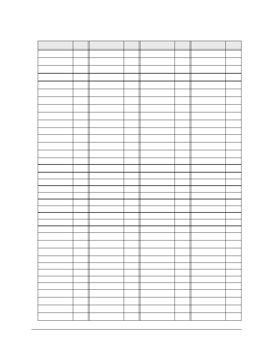
20
September 6, 2002
HWR.BSP15.DS.REV.H
BSP-15 Processor Datasheet
video_inb[0]
C11
b
sdadr[9]
AA24
pci_cbe[3]
V1
VddI/O
AD3
video_inb[1]
B11
b
sdadr[10]
AB26
pci_ad[24]
V3
VddI/O
AC4
video_inb[2]
A11
b
sdadr[11]
AD26
pci_ad[25]
U1
VddI/O
Y4
video_inb[3]
D12
b
sdadr[12]
AB24
pci_ad[26]
U4
VddI/O
V4
video_inb[4]
C12
b
sdadr[13]
AD25
pci_ad[27]
U3
VddI/O
R4
video_inb[5]
B12
b
sddata[32]
AC24
pci_ad[28]
U2
VddI/O
L4
video_inb[6]
A13
b
sddata[33]
AB23
pci_ad[29]
T3
VddI/O
H4
video_inb[7]
C13
b
aVss
AC22
pci_ad[30]
T2
Vss
A1
video_inb[8]
D13
b
aVss
AD23
pci_ad[31]
R3
Vss
B1
video_inb[9]
B13
b
aVdd_PLL2
AE24
pci_req#[0]
R2
Vss
B2
tcib_inuse
A14
aVdd_PLL2
AF25
pci_req#[1]
R1
Vss
A5
tcib_sync
B14
sdclk_byp_in
AC21
b
pci_req#[2]
P3
Vss
B9
tcib_clk
C14
pclk
AD22
c
pci_gnt#[0]
P1
Vss
A12
ntsc_inb_clk27
D14
coreclk_byp_in
AE23
b
pci_gnt#[1]
N1
Vss
A15
vsync
A16
pci_clk
AF24
pci_gnt#[2]
N2
Vss
B18
hsync
B15
sddata[34]
AD21
pclk_out
N3
d
Vss
A22
tms
B16
sddata[35]
AF23
pci_rst#
M2
Vss
A26
trst
C15
sddqm[4]
AF22
pci_inta#
M3
Vss
B25
aVss
A17
sddata[36]
AE21
pci_pme#
L1
Vss
C26
gdac_fscale
B17
sddata[37]
AC19
iic_sda
L2
Vss
E26
gdac_comp
C16
sddata[38]
AD20
iic_sck
L3
Vss
F25
aVdd_DAC
D16
sddata[39]
AF21
iic_select
K1
Vss
G26
gdac_green
C17
sddata[40]
AF20
iis_in_data
K3
Vss
J26
gdac_blue
A18
sddata[41]
AC18
iis_in_lr
J1
Vss
K25
gdac_red
A19
sddata[42]
AD19
iis_in_bclk
K4
Vss
L26
gdac_cvgg(aVss)
C18
sddata[43]
AE19
iis_out_data[0]
J2
b
Vss
N26
aVddx
D17
sddqm[5]
AD18
iis_out_data[1]
J3
b
Vss
P25
aVssx
B19
sddata[44]
AF19
iis_out_data[2]
H2
b
Vss
R26
tdi
A20
sddata[45]
AE18
iis_out_lr
G1
Vss
U26
tck
B20
sddata[46]
AD17
iis_out_bclk
H3
Vss
V25
tdo
C19
sddata[47]
AE17
iec958_in
G2
Vss
W26
no connection
A21
sddata[48]
AF17
iec958_out
G3
Vss
AA26
sddata[0]
B21
sddata[49]
AD16
rom_cs#
F1
Vss
AB25
sddata[1]
C20
sddata[50]
AF16
ntsc_out_hsync
F3
b
Vss
AC26
sddata[2]
D19
sddata[51]
AC15
ntsc_out_vsync
E1
b
Vss
AC25
sddata[3]
A23
sddqm[6]
AD15
ntsc_out_data[0]
E2
b
Vss
AE26
sddqm[0]
B22
sddata[52]
AE15
ntsc_out_data[1]
E3
b
Vss
AE25
Table 3-1 Pin Assignments (Continued)
Signal Name
Ball
Signal Name
Ball
Signal Name
Ball
Signal Name
Ball

21
September 6, 2002
HWR.BSP15.DS.REV.H
BSP-15 Processor Datasheet
.
sddata[4]
C21
sddata[53]
AF15
ntsc_out_data[2]
C1
b
Vss
AF26
sddata[5]
A24
sddata[54]
AD14
audioclk_out
C2
Vss
AE22
sddata[6]
B23
sddata[55]
AE14
pixelclk_out
D3
e
Vss
AE20
sddata[7]
C22
sddata[56]
AF13
Vddcore
D6
Vss
AF18
sddata[8]
D21
sddata[57]
AD13
Vddcore
D11
Vss
AE16
sddata[9]
A25
sddata[58]
AF12
Vddcore
D15
Vss
AF14
sddata[10]
B24
sddata[59]
AE12
Vddcore
D20
Vss
AE13
sddata[11]
C23
sddqm[7]
AD12
Vddcore
E23
Vss
AE11
sddqm[1]
D22
sddata[60]
AC12
Vddcore
G23
Vss
AF9
sddata[12]
D24
sddata[61]
AF11
Vddcore
H23
Vss
AE7
sddata[13]
B26
sddata[62]
AD11
Vddcore
K23
Vss
AE5
sddata[14]
C25
sddata[63]
AF10
Vddcore
M23
Vss
AF1
sddata[15]
E24
pci_ad[0]
AE10
Vddcore
P23
Vss
AE2
sddata[16]
D25
pci_ad[1]
AD10
Vddcore
T23
Vss
AD1
sddata[17]
D26
pci_ad[2]
AE9
Vddcore
V23
Vss
AB2
sddata[18]
E25
pci_ad[3]
AF8
Vddcore
W23
Vss
Y1
sddata[19]
F24
pci_ad[4]
AD9
Vddcore
AA23
Vss
V2
sddqm[2]
F26
pci_ad[5]
AE8
Vddcore
AC20
Vss
T1
sddata[20]
G24
pci_ad[6]
AC9
Vddcore
AC16
Vss
P2
sddata[21]
G25
pci_ad[7]
AD8
Vddcore
AC11
Vss
M1
sddata[22]
H25
pci_cbe_[0]
AF7
Vddcore
AC7
Vss
K2
sddata[23]
H24
pci_ad[8]
AF6
Vddcore
AB4
Vss
H1
sddata[24]
H26
pci_ad[9]
AD7
Vddcore
AA4
Vss
F2
sddata[25]
J24
pci_ad[10]
AC8
Vddcore
W4
Vss
D1
sddata[26]
J25
pci_ad[11]
AE6
Vddcore
T4
Vss
D2
a.
If unused,
NCi (Vss)
and tie to ground
b.
connect to 27 MHz or lower clock
c.
connect to 27 MHz clock
d.
If unused,
NCo and floating
e.
Leave floating
Table 3-1 Pin Assignments (Continued)
Signal Name
Ball
Signal Name
Ball
Signal Name
Ball
Signal Name
Ball
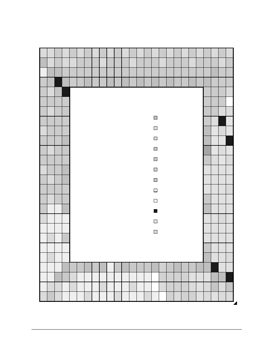
22
September 6, 2002
HWR.BSP15.DS.REV.H
BSP-15 Processor Datasheet
Vs
s
Vs
s
nt
s
c
_o
u
t
_
da
ta
[
2
]
Vs
s
nt
s
c
_o
u
t
_
vs
ync
rom
_
c
s
_
ii
s
_
o
u
t
_
lr
Vs
s
ii
s
_
in_
l
r
ii
c_
se
l
e
c
t
pc
i_
pm
e
_
Vs
s
pc
i_gn
t
_[1
]
pc
i_gn
t
_[0
]
pc
i_re
q
_[1
]
Vs
s
pc
i_a
d
[25
]
pc
i_
cb
e
_
[
3
]
pc
i_a
d
[22
]
Vs
s
pc
i_a
d
[19
]
pc
i_a
d
[16
]
pc
i_
cb
e
_
[
2
]
Vs
s
Vddc
ore
Vs
s
pc
i_
i
r
dy_
pc
i
_pa
r
Vs
s
pc
i
_
a
d
[12]
Vs
s
a
udi
oc
l
k
_
out
Vs
s
nt
s
c
_ou
t_
da
ta
[0]
Vs
s
i
e
c
958_
in
ii
s
_
out
da
ta
[2]
ii
s
_
out
da
ta
[0]
Vs
s
ii
c
_
s
d
a
pc
i_
r
s
t_
pc
i
_gnt
_[2]
Vs
s
pc
i
_
re
q
_[0]
pc
i
_
a
d
[30]
pc
i
_
a
d
[28]
Vs
s
pc
i
_
a
d
[23]
pc
i
_
a
d
[21]
pc
i
_
a
d
[17]
Vs
s
pc
i_
fra
m
e
_
Vs
s
Vs
s
pc
i_
st
o
p
_
aV
s
s
aV
d
d
Vd
dI/O
pix
e
lc
lk
_o
ut
nts
c
_out
_
da
t
a
[
1
]
nts
c
_out
_
hs
yn
c
i
e
c
958
_out
ii
s
_
ou
t
_bc
lk
ii
s
_
ou
t
da
t
a
[
1
]
ii
s
_
i
n
_da
ta
ii
c_s
c
k
pc
i
_
in
ta
_
pc
l
k_ou
t
pc
i_
re
q
_[2]
pc
i
_
a
d
[31]
pc
i
_
a
d
[29]
pc
i
_
a
d
[27]
pc
i
_
a
d
[24]
pc
i
_ids
e
l
pc
i
_
a
d
[20]
pc
i
_
a
d
[18]
Vs
s
Vd
dc
o
r
e
Vd
dI/O
pc
i
_
de
v
s
e
l
_
pc
i
_
a
d
[15]
nt
s
c
_o
u
t
_
da
ta
[
5
]
p
i
xe
lc
lk_
b
yp_
in
aV
s
s
VddI
/O
VddI
/O
VddI
/O
ii
s
_
in
_blk
VddI
/O
Vdd
c
ore
Vdd
c
ore
Vdd
c
ore
VddI
/O
Vdd
c
ore
pc
i_a
d
[2
6]
VddI
/O
Vdd
c
ore
VddI
/O
Vdd
c
ore
Vdd
c
ore
VddI
/O
pc
i_
t
r
dy_
pc
i_
c
b
e
[1]
pc
i_a
d
[1
3]
Vs
s
nt
s
c
_o
ut_
da
ta
[4]
nt
s
c
_o
ut_
da
ta
[3]
pc
i_s
e
rr
int
b
_
pc
i_
a
d
[14]
pc
i_
a
d
[1
1]
pc
i_
a
d
[8
]
vide
o_
ina
[
3]
vide
o_
ina
[
0]
nts
c
_out
_
da
ta
[6]
Vdd
c
or
e
pc
i_a
d
[9]
Vs
s
pc
i_
c
b
e
[0]
vi
de
o_
in
a
[
5
]
vi
de
o_
in
a
[
4
]
vi
de
o_
in
a
[
1
]
nts
c
_out
_
da
t
a
[7
]
pc
i_a
d
[10
]
pc
i_a
d
[7]
pc
i_a
d
[5]
pc
i_a
d
[3]
tc
ia
_
i
nus
e
vi
de
o
_
in
a[
8
]
vi
de
o
_
in
a[
6
]
vi
de
o
_
in
a[
2
]
pc
i_
a
d
[6
]
pc
i_
a
d
[4
]
pc
i_
a
d
[2
]
Vs
s
tc
ia
_
s
ync
Vs
s
vid
e
o_
ina
[
9]
vid
e
o_
ina
[
7]
Vdd
I
/O
pc
i_
a
d
[1]
pc
i_
a
d
[0]
s
dda
ta
[
63]
nt
s
c
_i
na
c
l
k27
tc
ia
_
vda
c
tc
ia
_cl
k
Vddc
ore
sd
d
a
t
a
[62
]
Vs
s
sd
d
a
t
a
[61
]
vi
de
o
_
i
nb[2]
vi
de
o
_
i
nb[1]
vi
de
o
_
i
nb[0]
sd
d
a
t
a
[60]
s
d
dqm
[7
]
sd
d
a
t
a
[59]
sd
d
a
t
a
[58]
Vs
s
vid
e
o_
in
b[5]
vid
e
o_
in
b[4]
vid
e
o_
in
b[3]
Vd
dI/O
s
dda
ta
[
57]
Vs
s
s
dda
ta
[
56]
v
i
de
o_
inb
[
6]
v
i
de
o_
inb
[
9]
v
i
de
o_
inb
[
7]
v
i
de
o_
inb
[
8]
sd
d
a
t
a
[5
4]
sd
d
a
t
a
[5
5]
Vs
s
tc
ib
_
i
nus
e
tc
ib
_
sy
n
c
tc
ib_c
lk
nts
c
_inb
_c
lk27
sd
d
a
t
a
[51]
s
ddqm
[6
]
sd
d
a
t
a
[52]
sd
d
a
t
a
[53]
Vs
s
hs
ync
tr
s
t
Vddc
ore
Vd
d
c
o
r
e
s
dda
ta
[49]
Vs
s
s
dda
ta
[50]
vs
yn
c
tm
s
gda
c
_
co
m
p
aV
d
d
_DAC
Vdd
I
/O
s
dda
ta
[4
6]
s
dda
ta
[4
7]
s
dda
ta
[4
8]
aV
s
s
gd
a
c
_
fs
c
a
l
e
gd
a
c
_
gre
e
n
a
V
ddx
sd
d
a
t
a
[41
]
s
ddqm
[5]
sd
d
a
t
a
[45
]
Vs
s
gda
c
_
bl
ue
Vs
s
g
d
ac_cvgg(
aV
ss
)
VddI/
O
s
dda
ta
[37]
s
dda
ta
[42]
s
dda
ta
[43]
s
dda
ta
[44]
gda
c
_
re
d
aV
s
s
x
tdo
s
dda
ta
[2
]
Vdd
c
or
e
s
dda
ta
[
38]
Vs
s
s
dda
ta
[
40]
tdi
tc
k
s
dda
ta
[1]
Vdd
c
or
e
sd
c
l
k
_
by
p_in
sd
d
a
t
a
[34
]
sd
d
a
t
a
[36
]
sd
d
a
t
a
[39
]
n
o
c
on-
ne
c
t
i
o
n
sd
d
a
t
a
[0]
sd
d
a
t
a
[4]
sd
d
a
t
a
[8]
aV
s
s
pc
lk
Vs
s
s
d
dqm
[4
]
Vs
s
s
d
dqm
[0
]
s
dda
ta
[7
]
s
d
dqm
[1
]
s
dda
ta
[3]
s
dda
ta
[6]
s
dda
ta
[1
1]
Vd
dI/O
Vd
dc
o
r
e
Vd
dI/O
Vd
dc
o
r
e
Vd
dc
o
r
e
Vd
dI/O
Vd
dc
o
r
e
Vd
dI/O
Vd
dc
o
r
e
Vd
dI/O
Vd
dc
o
r
e
Vd
dI/O
Vd
dc
o
r
e
Vd
dI/O
Vd
dc
o
r
e
Vd
dc
o
r
e
Vd
dI/O
Vd
dc
o
r
e
s
dda
ta
[
33]
Vd
dI/O
aV
s
s
co
r
e
c
l
k
_
byp_i
n
s
dda
ta
[
35]
sd
d
a
t
a
[5]
sd
d
a
t
a
[1
0]
VddI
/O
sd
d
a
t
a
[1
2]
sd
d
a
t
a
[1
5]
sd
d
a
t
a
[1
9]
sd
d
a
t
a
[2
0]
sd
d
a
t
a
[2
3]
sd
d
a
t
a
[2
5]
sd
d
a
t
a
[2
7]
sd
d
a
t
a
[2
8]
sd
d
a
t
a
[3
1]
sd
c
s
_
[1]
sd
r
t
n
c
l
k
sd
c
l
k
1
sd
c
a
s#
s
d
a
d
r[0]
s
d
a
d
r[2]
s
d
a
d
r[5]
s
d
a
d
r[7]
s
d
a
d
r[9]
sd
a
d
r
[1
2]
sd
d
a
t
a
[3
2]
VddI
/O
aV
d
d
_P
L
L
2
pc
i
_
c
l
k
sd
d
a
t
a
[9
]
Vs
s
sd
d
a
t
a
[14]
sd
d
a
t
a
[16]
sd
d
a
t
a
[18]
Vs
s
sd
d
a
t
a
[21]
sd
d
a
t
a
[22]
sd
d
a
t
a
[26]
Vs
s
sd
d
a
t
a
[29]
sd
d
a
t
a
[30]
sd
c
s
_
[2
]
Vs
s
sd
c
l
k
sd
r
a
s#
sd
w
e
#
Vs
s
sd
a
d
r
[
3
]
sd
a
d
r
[
6
]
sd
a
d
r
[
8
]
Vs
s
Vs
s
sd
a
d
r
[13]
Vs
s
aV
d
d
_P
L
L
2
Vs
s
s
dda
ta
[13]
Vs
s
s
dda
ta
[17]
Vs
s
sd
d
q
m
[2
]
Vs
s
s
dda
ta
[24]
Vs
s
sd
d
q
m
[3
]
Vs
s
sd
c
s
_
[0
]
Vs
s
sd
c
s
_
[3
]
Vs
s
sd
c
l
k
2
Vs
s
s
d
a
d
r[1]
Vs
s
s
d
a
d
r[4]
Vs
s
sd
a
d
r
[10]
Vs
s
sd
a
d
r
[1
1]
Vs
s
Vs
s
a
udi
oc
l
k
_
byp
_in
VddI
/O
A
B
C
D
E
F
G
H
J
K
L
M
N
P
R
T
U
V
W
Y
AA
AB
AC
AD
AE
AF
A
B
C
D
E
F
G
H
J
K
L
M
N
P
R
T
U
V
W
Y
AA
AB
AC
AD
AE
AF
1
2
3
4
5
6
7
8
9
10
11
12
13
14
15
16
17
18
19
20
21
22
23
24
25
26
1
2
3
4
5
6
7
8
9
10
11
12
13
14
15
16
17
18
19
20
21
22
23
24
25
26
Vd
d
c
o
r
e
Vddc
ore
Vd
d
c
o
r
e
Vd
d
c
o
r
e
Vddc
ore
V
ddI/
O
aV
d
d
VddI/O
Multi-function pins
Vss
Vddcore
CRT (DRC)
aVss
JTAG
SDRAM
PLLs
PCI
IIC
IIS
Figure 3.1 BSP-15 DSP pins viewed from bottom
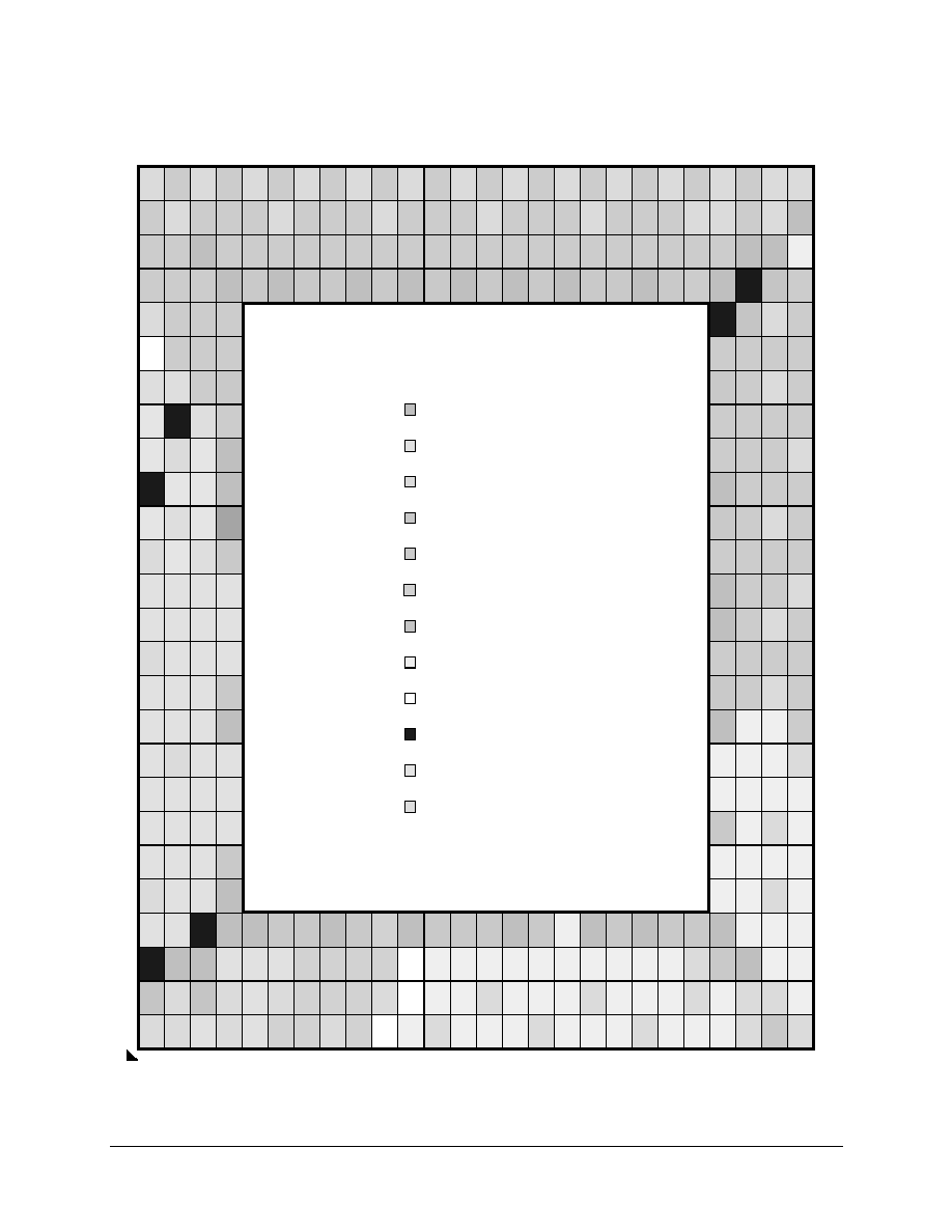
23
September 6, 2002
HWR.BSP15.DS.REV.H
BSP-15 Processor Datasheet
Vs
s
Vs
s
nt
s
c
_o
u
t
_
da
ta
[
2
]
Vs
s
nt
s
c
_o
u
t
_
vs
ync
rom
_
c
s
_
ii
s
_
o
u
t
_
lr
Vs
s
ii
s
_
in_
l
r
ii
c_
se
l
e
c
t
pc
i_
pm
e
_
Vs
s
pc
i_g
n
t
_[
1]
pc
i_g
n
t
_[
0]
pc
i_re
q
_[
1]
Vs
s
pc
i_a
d
[2
5]
pc
i_
cb
e
_
[
3
]
pc
i_a
d
[2
2]
Vs
s
pc
i_a
d
[1
9]
pc
i_a
d
[1
6]
pc
i_
cb
e
_
[
2
]
Vs
s
Vdd
c
ore
Vs
s
pc
i
_
ir
dy
_
pc
i_p
a
r
Vs
s
pc
i_
a
d
[
12]
Vs
s
a
u
dioc
lk
_
ou
t
Vs
s
nts
c
_out
_
da
t
a
[
0
]
Vs
s
ie
c
9
58_i
n
ii
s
_
ou
t
da
t
a
[
2
]
ii
s
_
ou
t
da
t
a
[
0
]
Vs
s
ii
c_s
d
a
pc
i_rs
t
_
pc
i_
gnt
_[
2
]
Vs
s
pc
i_
re
q
_[
0
]
pc
i_
a
d
[
30]
pc
i_
a
d
[
28]
Vs
s
pc
i_
a
d
[
23]
pc
i_
a
d
[
21]
pc
i_
a
d
[
17]
Vs
s
pc
i
_
fra
m
e
_
Vs
s
Vs
s
pc
i
_
st
o
p
_
aV
s
s
aV
d
d
VddI/
O
pi
xe
l
c
l
k_o
ut
nt
s
c
_ou
t_
da
ta
[1]
nt
s
c
_ou
t_
hs
ync
ie
c
958
_o
ut
ii
s
_
out
_b
c
l
k
ii
s
_
out
da
ta
[1]
ii
s
_
in
_d
a
t
a
ii
c_
s
c
k
pc
i_
int
a
_
pc
lk_
out
pc
i_
r
e
q
_[2]
pc
i
_
a
d
[31]
pc
i
_
a
d
[29]
pc
i
_
a
d
[27]
pc
i
_
a
d
[24]
pc
i
_id
s
e
l
pc
i
_
a
d
[20]
pc
i
_
a
d
[18]
Vs
s
Vddc
ore
VddI/
O
pc
i_
de
v
s
e
l
_
pc
i
_
a
d
[15]
nt
s
c
_
out_
da
ta
[
5
]
pi
xe
lc
lk_b
yp_i
n
aV
s
s
VddI/
O
VddI/
O
VddI/
O
ii
s
_
in
_b
l
k
VddI/
O
Vddc
ore
Vddc
ore
Vddc
ore
VddI/
O
Vddc
ore
pc
i_a
d
[26
]
VddI/
O
Vddc
ore
VddI/
O
Vddc
ore
Vddc
ore
VddI/
O
pc
i_
t
r
dy_
pc
i_c
b
e
[1]
pc
i_a
d
[13
]
Vs
s
nts
c
_out
_
da
t
a
[4
]
nts
c
_out
_
da
t
a
[3
]
pc
i_s
e
rr
int
b
_
pc
i_
a
d
[14]
pc
i_
a
d
[1
1]
pc
i_
a
d
[8
]
vide
o_
ina
[
3]
vide
o_
ina
[
0]
nt
s
c
_ou
t_
da
ta
[6]
Vddc
ore
pc
i_a
d
[9]
Vs
s
pc
i_c
b
e
[0]
vi
de
o
_
in
a[
5
]
vi
de
o
_
in
a[
4
]
vi
de
o
_
in
a[
1
]
nt
s
c
_o
ut_
da
ta
[7]
pc
i_a
d
[1
0]
pc
i_a
d
[7]
pc
i_a
d
[5]
pc
i_a
d
[3]
tc
i
a
_
inus
e
vi
de
o_
in
a
[
8
]
vi
de
o_
in
a
[
6
]
vi
de
o_
in
a
[
2
]
pc
i_
a
d
[6
]
pc
i_
a
d
[4
]
pc
i_
a
d
[2
]
Vs
s
tc
ia
_
s
ync
Vs
s
vide
o_
ina
[
9]
vide
o_
ina
[
7]
VddI/
O
pc
i
_
a
d
[1
]
pc
i
_
a
d
[0
]
sd
d
a
t
a
[63]
nts
c
_ina
c
l
k2
7
tc
ia
_
vda
c
t
c
ia
_c
lk
Vdd
c
ore
s
dda
t
a
[6
2]
Vs
s
s
dda
t
a
[6
1]
vi
de
o_
i
nb[2
]
vi
de
o_
i
nb[1
]
vi
de
o_
i
nb[0
]
s
dda
ta
[
60]
sd
d
q
m
[7]
s
dda
ta
[
59]
s
dda
ta
[
58]
Vs
s
v
i
de
o_
inb
[
5]
v
i
de
o_
inb
[
4]
v
i
de
o_
inb
[
3]
VddI/
O
sd
d
a
t
a
[57]
Vs
s
sd
d
a
t
a
[56]
vid
e
o_
in
b[6]
vid
e
o_
in
b[9]
vid
e
o_
in
b[7]
vid
e
o_
in
b[8]
sd
d
a
t
a
[54
]
sd
d
a
t
a
[55
]
Vs
s
tc
ib
_
i
nus
e
tc
ib
_
sy
n
c
tc
ib
_
c
l
k
nts
c
_inb
_c
l
k27
s
dda
ta
[
51]
s
ddq
m
[6]
s
dda
ta
[
52]
s
dda
ta
[
53]
Vs
s
hs
y
n
c
tr
s
t
Vd
dc
or
e
Vddc
ore
s
dda
ta
[49]
Vs
s
s
dda
ta
[50]
vs
ync
tm
s
gda
c
_
co
m
p
aV
d
d
_
DAC
VddI/
O
sd
d
a
t
a
[46
]
sd
d
a
t
a
[47
]
sd
d
a
t
a
[48
]
aV
s
s
g
d
ac_
fs
c
a
l
e
g
d
ac_
gre
e
n
aV
d
d
x
s
dda
ta
[4
1]
s
ddq
m
[5]
s
dda
ta
[4
5]
Vs
s
gd
a
c
_
bl
u
e
Vs
s
gdac_cv
gg(
aV
ss
)
Vdd
I
/O
s
dda
ta
[37]
s
dda
ta
[42]
s
dda
ta
[43]
s
dda
ta
[44]
gda
c
_
re
d
a
V
ssx
tdo
s
dda
ta
[2
]
Vddc
ore
sd
d
a
t
a
[38]
Vs
s
sd
d
a
t
a
[40]
td
i
tc
k
sd
d
a
t
a
[1]
Vddc
ore
sd
c
l
k
_
b
yp_i
n
s
dda
t
a
[3
4]
s
dda
t
a
[3
6]
s
dda
t
a
[3
9]
no c
on-
ne
c
t
ion
s
dda
t
a
[0]
s
dda
t
a
[4]
s
dda
t
a
[8]
aV
s
s
pc
l
k
Vs
s
sd
d
q
m
[4]
Vs
s
sd
d
q
m
[0]
s
dda
ta
[7]
sd
d
q
m
[1]
sd
d
a
t
a
[3
]
sd
d
a
t
a
[6
]
sd
d
a
t
a
[1
1]
VddI/
O
Vddc
ore
VddI/
O
Vddc
ore
Vddc
ore
VddI/
O
Vddc
ore
VddI/
O
Vddc
ore
VddI/
O
Vddc
ore
VddI/
O
Vddc
ore
VddI/
O
Vddc
ore
Vddc
ore
VddI/
O
Vddc
ore
sd
d
a
t
a
[33]
VddI/
O
aV
s
s
co
r
e
c
l
k
_
byp
_in
sd
d
a
t
a
[35]
sd
d
a
t
a
[5]
sd
d
a
t
a
[10
]
VddI
/O
sd
d
a
t
a
[12
]
sd
d
a
t
a
[15
]
sd
d
a
t
a
[19
]
sd
d
a
t
a
[20
]
sd
d
a
t
a
[23
]
sd
d
a
t
a
[25
]
sd
d
a
t
a
[27
]
sd
d
a
t
a
[28
]
sd
d
a
t
a
[31
]
sd
c
s
_
[1]
sd
r
t
n
c
l
k
sd
c
l
k
1
sd
c
a
s#
s
d
a
d
r[0]
s
d
a
d
r[2]
s
d
a
d
r[5]
s
d
a
d
r[7]
s
d
a
d
r[9]
sd
a
d
r
[12
]
sd
d
a
t
a
[32
]
VddI
/O
aV
d
d
_
P
LL2
pc
i
_
c
l
k
s
dda
ta
[9]
Vs
s
s
dda
ta
[
14]
s
dda
ta
[
16]
s
dda
ta
[
18]
Vs
s
s
dda
ta
[
21]
s
dda
ta
[
22]
s
dda
ta
[
26]
Vs
s
s
dda
ta
[
29]
s
dda
ta
[
30]
sd
c
s
_
[2]
Vs
s
sd
c
l
k
sd
r
a
s
#
sd
w
e
#
Vs
s
s
d
a
d
r[3]
s
d
a
d
r[6]
s
d
a
d
r[8]
Vs
s
Vs
s
sd
a
d
r
[
13]
Vs
s
aV
d
d
_P
L
L
2
Vs
s
s
dda
ta
[13]
Vs
s
s
dda
ta
[17]
Vs
s
s
d
dqm
[2
]
Vs
s
s
dda
ta
[24]
Vs
s
s
d
dqm
[3
]
Vs
s
sd
c
s
_
[0
]
Vs
s
sd
c
s
_
[3
]
Vs
s
sd
c
l
k
2
Vs
s
s
d
a
d
r[1
]
Vs
s
s
d
a
d
r[4
]
Vs
s
sd
a
d
r
[10]
Vs
s
sd
a
d
r
[1
1]
Vs
s
Vs
s
a
u
dioc
lk
_
byp_i
n
VddI
/O
A
B
C
D
E
F
G
H
J
K
L
M
N
P
R
T
U
V
W
Y
AA
AB
AC
AD
AE
AF
A
B
C
D
E
F
G
H
J
K
L
M
N
P
R
T
U
V
W
Y
AA
AB
AC
AD
AE
AF
1
2
3
4
5
6
7
8
9
1
0
1
1
12
1
3
14
15
1
6
17
18
1
9
20
21
2
2
23
24
2
5
26
1
2
3
4
5
6
7
8
9
1
0
1
1
12
1
3
14
15
1
6
17
18
1
9
20
21
2
2
23
24
2
5
26
Vddc
ore
Vdd
c
or
e
Vddc
ore
Vddc
ore
Vdd
c
ore
Vdd
I
/O
aV
d
d
VddI/O
Multi-function pins
Vss
Vddcore
CRT (DRC)
aVss
JTAG
SDRAM
PLLs
PCI
IIC
IIS
Figure 3.2 BSP-15 DSP pins viewed from top

24
September 6, 2002
HWR.BSP15.DS.REV.H
BSP-15 Processor Datasheet
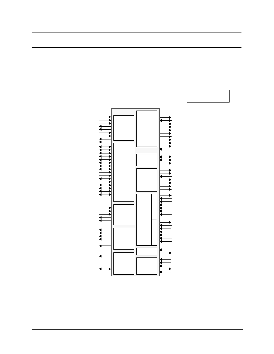
HWR.BSP15.DS.REV.H
BSP-15 Processor Datasheet
September 6, 2002
25
Chapter 4
Signal Descriptions
4.1 Interface Summary
Processor
Clock
(PLL)
BSP-15
chip
PCI
pclk
coreclk_byp_in
pixelclk_byp_in / xmt_clk
audioclk_out
tcia_vdac
sdclk_byp_in
audioclk_byp_in
pclk_out
pixelclk_ou
pci_ad[31:0]
pci_cbe[3:0]
pci_frame#
pci_trdy#
pci_irdy#
pci_stop#
pci_par
pci_devsel#
pci_clk
pci_rst#
pci_inta#
pci_idsel
pci_req#[2:0]
pci_gnt#[2:0]
pci_serr_intb#
pci_pme#
iis_in_data
iis_in_lr
iis_in_bclk
iis_out_lr
iis_out_bclk
IIS
(rom_oe#)/iis_out_data[2]
(rom_wrt#)/iis_out_data[1]
(rom_ale)/iis_out_data[0]
rom_cs#
Flash
ROM
Video
Output
SDRAM
Controller
sdadr[13:0]
sddata[63:0]
sdcs[3:0]#
sdras#
sdcas#
sdwe#
sddqm[7:0]
sdclk
sdclk1
sdclk2
sdrtnclk
IIC
iic_sda
iic_sck
iic_select
gdac_fscale
gdac_comp
gdac_blue
gdac_green
gdac_red
vsync
hsync
CRT
(DRC)
tcib_inuse
tcib_sync
tcib_clk
tcib_err# / ntsc_inb_vsync
tcib_enable / ntsc_inb_hsync
tcib_data[7:0] / ntsc_inb_data[7:0]
ntsc_inb_clk27
tcia_inuse
tcia_sync
tcia_clk
tcia_err# / ntsc_ina_vsync / xmt_ack
tcia_enable / ntsc_ina_hsync / rcv_req
tcia_data[7:0] / ntsc_ina_data[7:0] / rcv_data_in[7:0]
ntsc_ina_clk27 / rcv_clk
Video
Input
i
n
put
A
i
npu
t
B
IEC958
iec958_in
iec958_out
JTAG
tck
tms
tdi
tdo
trst
(rom_addr[19]/rom_addr[21]/rom_addr[1])/
ntsc_out_hsync / xmt_req
(rom_addr[18]/rom_addr[20]/rom_addr[0])/
ntsc_out_vsync / rcv_ack
<reset_strap[7:0]>/
(rom_addr[9:2]/rom_addr[17:10]/rom_data[7:0])/
ntsc_out_data[7:0] / xmt_data_out[7:0]
( ) --- valid during boot-up
< > --- valid during reset
# --- active low signal
Figure 4.1 BSP-15 Interface
26
BSP-15 Processor Datasheet
HWR.BSP15.DS.REV.H
September 6, 2002
4.2 Legend
A........................................... analog signal
B ........................................... bi-directional
I ............................................ input
O........................................... output
od.......................................... open drain or active pull down
trailing "#" ........................... active low
()........................................... parentheses indicate number of shared signal pins
4.3 Processor Clock
There is a single 27 MHz reference clock signal for generating internal clocks.
Table 4-1 Processor clock signal description
Signal
# of
Pins
I/O
Description
pclk
1
I
27 MHz VCXO input that serves as the reference signal to the three on-chip
PLLs. It is also a reference clock for the video output and the IIC interface
coreclk_byp_in
1
I
Bypass input for the core clock
sdclk_byp_in
1
I
Bypass input for the SDRAM clock.
pixelclk_byp_in
1
I
Transmit clock for GPDP (xmt_clk) or PLL-bypass input for pixel clock
audioclk_byp_in
1
I
Bypass input for the audio clock.
pclk_out
(coreclk_out)
1
O
Output for the core clock.
pixelclk_out
1
O
Output for the pixel clock.
audioclk_out
1
O
Audio clock output used for IIS interface master MCLK
tcia_vdac
1
O
Sigma-delta output from software loop filter for controlling external VCXO
for pclk
TOTAL
9
27
September 6, 2002
HWR.BSP15.DS.REV.H
BSP-15 Processor Datasheet
4.4 SDRAM
The
BSP-15
DSP supports either a SDRAM or SGRAM memory system using the signals shown
in
Table 4-2
. The
BSP-15
DSP supports a memory system of 64-bit or 32-bit data width. The
BSP-15
DSP supports DRAM widths of 8-bit, 16-bit or 32-bits.
4.5 PCI Bus
The
BSP-15
DSP provides the PCI bus as the primary system interface. 4-3 lists the PCI signals.
Table 4-2 Memory interface signals
Signal
# of
Pins
I/O
Description
sdadr[13:0]
14
O
Address lines indicate row addresses when sdras_ is active and indicate
column addresses when sdcas_ is active
sddata[63:0]
64
B
Data Input/Output lines transfer data between the memory and BSP-15
DSP. These are also input mask bits for Write-per-Bit. When block write
is activated, these lines provide column address mask
sdcs_[3:0]
4
O
Chip Select signal lines indicate that the command on the output lines is
for each memory chip. If this signal is high, the output command(s) will
be ignored by each corresponding memory chip
sdras#
1
O
sdras_ is part of the output command to the SDRAM/SGRAM
sdcas#
1
O
sdcas_ is part of the output command to the SDRAM/SGRAM
sdwe#
1
O
Write enable (sdwe_) is part of the output command
sddqm[7:0]
8
O
During read, sddqm = 1 turns off the output buffers of
SDRAM/SGRAM. During write, sddqm = 1 prevents a write to the
current memory location
sdclk, sdclk1,
sdclk2
3
O
sdclk, sdclk1, and sdclk2 are driven by the BSP-15 DSP's SDRAM
clock. All SDRAM/SGRAM input signals are sampled on the positive
edge of sdclk
sdrtnclk
1
I
sdrtnclk is driven by sdclk. This signal is used for latching the data from
SDRAM/SGRAM
TOTAL
97
Table 4-3 PCI interface signals
Signal
# of
Pins
I/O
Description
pci_ad[31:0]
32
B
PCI multiplexed address and data lines. The address is driven when
pci_frame_ is first asserted. Data is transferred on this bus in subsequent
clocks.
pci_cbe[3:0]
4
B
For PCI cycles, the bus command and byte enables are used to transfer the
PCI command during the address phase and are used to transfer byte lane
enables during subsequent data phases.

28
BSP-15 Processor Datasheet
HWR.BSP15.DS.REV.H
September 6, 2002
pci_frame#
1
B
Transaction framing for PCI transfers. The initial assertion indicates the
address phase and the start of a PCI transaction. Continued assertion
determines the burst size of the transaction.
pci_trdy#
1
B
The target ready signal is asserted when the PCI target is ready for a data
transfer.
pci_irdy#
1
B
The initiator ready signal is asserted when the PCI master is ready for a data
transfer.
pci_stop#
1
B
pci_stop_ is asserted by the target to request the master to stop the current
transaction.
pci_par
1
B
A single parity bit is calculated over pci_ad[31:0], and pci_c_be[3:0] and
transferred over this signal.
pci_devsel#
1
B
A target asserts the pci_devsel_ signal line to indicate it has decoded the
address on the pci_ad[31:0] bus and will participate in (claim) the current
transaction. The PCI bus master must monitor the pci_devsel_ signal line to
determine if a target bus has claimed the transaction or if it will execute a
Master Abort termination. pci_devsel_ will be tri-stated from the leading
edge of pci_rst_. pci_devsel_ remains tri-stated until driven by the target.
pci_clk
1
I
pci_clk provides timing for all PCI transactions on the PCI bus. All other
PCI signals are sampled on the rising edge of pci_clk, and all timing
parameters are defined with respect to this edge.
NOTE:
The BSP-15 DSP's core clock PLL does not use this clock
as a core PLL reference clock.
pci_rst#
1
I
This signal indicates a reset of all PCI resources. In addition, the internal
BSP-15 DSP core, etc. are reset by the assertion of this signal. PCI pad cell
drivers are disabled by the assertion of this signal, as specified in the PCI
2.1 document.
pci_inta#
1
B (od)
When the BSP-15 DSP is not designated as the PCI bus "HOST", then this
signal is the open drain output generating an asynchronous level sensitive
interrupt on the PCI bus. The BSP-15 DSP pad cell does not contain a pull
up for this signal.
When the BSP-15 DSP is designated as the PCI bus "HOST" then this
signal is an interrupt request input from PCI devices. The BSP-15 DSP sees
and utilizes this interrupt.
pci_idsel
1
I
The initialization device select is used as a slot addressed chip select input
during configuration read and write transactions. This signal is inactive in a
self-hosted configuration.
pci_req#[2:0]
3
B
The assertion of pci_req_ in a non-self-hosted configuration indicates that
the BSP-15 DSP desires the use of the PCI bus.
pci_gnt#[2:0]
3
B
The assertion of pci_gnt_ in a non-self-hosted environment indicates that
the BSP-15 DSP has been granted the use of the PCI bus.
Table 4-3 PCI interface signals
Signal
# of
Pins
I/O
Description

29
September 6, 2002
HWR.BSP15.DS.REV.H
BSP-15 Processor Datasheet
4.6 IEC958
The
BSP-15
DSP provides an IEC958 interface as shown in
Table 4-4
.
4.7 IIS
The
BSP-15
DSP provides interfaces for IIS digital audio input and output as shown in
Table 4-5
.
pci_serr_intb#
1
B (od)
This open drain output may generate either an asynchronous level sensitive
interrupt or the PCI bus or optionally signal SYSTEM ERROR. See the
BSP-15 DSP configuration control register for the signal's current use.
When the BSP-15 DSP is not designated as the PCI bus "HOST", then this
signal is the open drain output generating an asynchronous level sensitive
interrupt on the PCI bus. The BSP-15 DSP's pad cell does not contain a pull
up for this signal.
When the BSP-15 DSP is designated as the PCI bus "HOST", then this
signal is an interrupt request input from PCI devices. The BSP-15 DSP sees
and utilizes this interrupt.
pci_pme#
1
B (od)
When BSP-15 DSP is not in PCI host mode, this signal is an open drain
output used to request a change in power management state.
When BSP-15 DSP is in PCI host mode, this is an input signal to which PCI
devices indicate changes in power management state.
TOTAL
54
Table 4-4 IEC958 interface signals
Signal
# of
Pins
I/O
Description
iec958_in
1
I
Serial input line for IEC958 digital audio.
iec958_out
1
O
Serial output line for IEC958 digital audio.
TOTAL
2
Table 4-5 IIS interface signals
Signal
# of
Pins
I/O
Description
iis_in_data
1
I
Serial data input
iis_in_lr
1
I
Select left/right channel in the serial input
iis_in_bclk
1
I
IIS input bit clock
tcia_vdac
1
O
Serial output data (1 stereo channel)
Requires IIS bypass mode to be activated and and disables
channel 1 and 2.
Table 4-3 PCI interface signals
Signal
# of
Pins
I/O
Description
30
BSP-15 Processor Datasheet
HWR.BSP15.DS.REV.H
September 6, 2002
4.8 Multi-Function Signal Pins
Table 4-6
lists the pin name and pin number of the shared pins on the BSP-15 DSP, along with the
signal name associated with each mode-specific function.
iis_out_data[2:0]
3
O
Serial output data (3 stereo channels)
iis_out_lr
1
O
Select left/right channel in serial output channels
iis_out_bclk
1
O
IIS output bit-rate clock
TOTAL
a
8
a.
audioclk_out, defined in Section 4.3 on page 26, serves as the output MCLK in master mode.
Table 4-6 Multiple Signal Pins
Ball
#
Pin Name
ITU-656
Mode
TCI
Mode
GPDP
Mode
dRGB
Mode
ROM Boot
Mode
Reset
Mode
B4 pixelclk_byp_in
-
-
xmt_clk
-
-
B6
video_ina[0]
ntsc_ina_data[0] tcia_data[0]
rcv_data_in[0]
dRGB12.G4
-
-
C7
video_ina[1]
ntsc_ina_data[1] tcia_data[1]
rcv_data_in[1]
dRGB12.G5
-
-
D8
video_ina[2]
ntsc_ina_data[2] tcia_data[2]
rcv_data_in[2]
dRGB12.G6
-
-
A6
video_ina[3]
ntsc_ina_data[3] tcia_data[3]
rcv_data_in[3]
dRGB12.G7
-
-
B7
video_ina[4]
ntsc_ina_data[4] tcia_data[4]
rcv_data_in[4]
dRGB12.R4
-
-
A7
video_ina[5]
ntsc_ina_data[5] tcia_data[5]
rcv_data_in[5]
dRGB12.R5
-
-
C8
video_ina[6]
ntsc_ina_data[6] tcia_data[6]
rcv_data_in[6]
dRGB12.R6
-
-
D9
video_ina[7]
ntsc_ina_data[7] tcia_data[7]
rcv_data_in[7]
dRGB12.R7
-
-
B8
video_ina[8]
ntsc_ina_hsync
tcia_enable
rcv_req
dRGB18.B2
-
-
C9
video_ina[9]
ntsc_ina_vsync
tcia_err#
xmt_ack
dRGB18.B3
-
-
A10
ntsc_ina_clk27
-
-
rcv_clk
-
-
-
C11
video_inb[0]
ntsc_inb_data[0
]
tcib_data[0]
-
-
-
-
B11
video_inb[1]
ntsc_inb_data[1
]
tcib_data[1]
-
-
-
-
A11
video_inb[2]
ntsc_inb_data[2
]
tcib_data[2]
-
-
-
-
D12
video_inb[3]
ntsc_inb_data[3
]
tcib_data[3]
-
-
-
-
C12
video_inb[4]
ntsc_inb_data[4
]
tcib_data[4]
-
-
-
-
B12
video_inb[5]
ntsc_inb_data[5
]
tcib_data[5]
-
-
-
-
A13
video_inb[6]
ntsc_inb_data[6
]
tcib_data[6]
-
-
-
-
C13
video_inb[7]
ntsc_inb_data[7
]
tcib_data[7]
-
-
-
-
D13
video_inb[8]
ntsc_inb_hsync
tcib_enable
-
dRGB18.R2
-
-
Table 4-5 IIS interface signals
Signal
# of
Pins
I/O
Description

31
September 6, 2002
HWR.BSP15.DS.REV.H
BSP-15 Processor Datasheet
4.8.1 Transport Channel Interfaces (TCI)
The
BSP-15
DSP provides two parallel/serial TCI interfaces. See
Table 4-7
and
Table 4-8
.
B13
video_inb[9]
ntsc_inb_vsync
tcib_err#
-
dRGB18.R3
-
-
J2
iis_out_data[0]
-
-
-
-
rom_ale
-
J3
iis_out_data[1]
-
-
-
-
rom_wrt#
-
H2
iis_out_data[2]
-
-
-
-
rom_ole#
-
F3
ntsc_out_hsync
-
-
xmt_req
dRGB18.G2
rom_addr[21,19,1]
-
E1
ntsc_out_vsync
-
-
rcv_ack
dRGB18.G3
rom_addr[20,18,0]
-
E2 ntsc_out_data[0]
-
-
xmt_data_out[0] dRGB24.G0
rom_addr[2,10]/rom_data[0
]
reset_strap[0]
E3 ntsc_out_data[1]
-
-
xmt_data_out[1] dRGB24.G1
rom_addr[3,11]/rom_data[1
]
reset_strap[1]
C1 ntsc_out_data[2]
-
-
xmt_data_out[2]
rom_addr[4,12]/rom_data[2
]
reset_strap[2]
C5 ntsc_out_data[3]
-
-
xmt_data_out[3]
rom_addr[5,13]/rom_data[3
]
reset_strap[3]
B5 ntsc_out_data[4]
-
-
xmt_data_out[4] dRGB24.R0
rom_addr[6,14]/rom_data[4
]
reset_strap[4]
A4 ntsc_out_data[5]
-
-
xmt_data_out[5] dRGB24.R1
rom_addr[7,15]/rom_data[5
]
reset_strap[5]
C6 ntsc_out_data[6]
-
-
xmt_data_out[6] dRGB24.B0
rom_addr[8,16]/rom_data[6
]
reset_strap[6]
D7 ntsc_out_data[7]
-
-
xmt_data_out[7] dRGB24.B1
rom_addr[9,17]/rom_data[7
]
reset_strap[7]
A9
tcia_sync
-
-
-
dRGB12.B7
-
-
B14
tcib_sync
-
-
-
dRGB12.B6
-
-
A8
tcia_inuse
-
-
-
dRGB12.B5
-
-
A14
tcib_inuse
-
-
-
dRGB12.B4
-
-
B10
tcia_vdac
-
tcia_vdac-
-
iis_out_data
[0]
a
-
-
G3
iec958_out
-
-
-
blank
-
-
a.
if IIS bypass mode enabled
Table 4-7 Primary TCI Interface Signals
Signal
# of
Pins
I/O
Description
tcia_data[7:0]
(8)
I
TCI data input: All 8 bits of input are used in parallel mode. Only tci_data[0] is
used in serial mode
tcia_enable
(1)
I
Transport channel enable:
1 = accept a TCI input sample
0 = ignore TCI input sample
tcia_inuse
1
O
Video input port external mux select. This pin can also be used as a general
purpose output if dynamic muxing of the video input is not required.
Table 4-6 Multiple Signal Pins (Continued)
Ball
#
Pin Name
ITU-656
Mode
TCI
Mode
GPDP
Mode
dRGB
Mode
ROM Boot
Mode
Reset
Mode
32
BSP-15 Processor Datasheet
HWR.BSP15.DS.REV.H
September 6, 2002
4.8.2 ITU-656 Inputs
Analog video can be digitized according to ITU-R BT.601/656 via a NTSC, PAL or SVIDEO
decoder and then input to the
BSP-15
DSP. The interface signals for the primary and secondary
video inputs are shown in
Table 4-9
and
Table 4-10
.
tcia_sync
1
I
Demodulator/FEC has marked the synchronization point in the MPEG2
transport stream packet. The packet size is programmable.
tcia_err_#
(1)
I
This active low signal indicates that the Demodulator/FEC has detected an
uncorrectable error in the current packet.
tcia_clk
1
I
Transport channel clock
TOTAL
3(10)
Table 4-8 Secondary TCI Interface Signals
Signal
# of
Pins
I/O
Description
tcib_data[7:0]
(8)
I
TCI data input: All 8-bits of input are used in parallel mode. Only tci_data[0]
is used in serial mode.
tcib_enable
(1)
I
Transport channel enable:
1 = accept a TCI input sample
0 = ignore TCI input sample
tcib_inuse
1
O
Video input port external mux select. This pin can also be used as a general
purpose output if dynamic muxing of the video input is not required.
tcib_sync
1
I
Demodulator/FEC has marked the synchronization point in the MPEG2
transport stream packet. The packet size is programmable.
tcib_err#
(1)
I
This active low signal indicates that the Demodulator/FEC has detected an
uncorrectable error in the current packet.
tcib_clk
1
I
Transport channel clock
TOTAL
3(10)
Table 4-9 Primary ITU-R BT.601/656 Input Interface Signals
Signal
# of
Pins
I/O
Description
ntsc_ina_clk27
1
I
27 MHz clock from video decoder
ntsc_ina_hsync
(1)
I
Horizontal sync
ntsc_ina_vsync
(1)
I
Vertical sync
ntsc_ina_data[7:0]
(8)
I
ITU-R BT.601/656 formatted video input stream
TOTAL
1(10)
Table 4-7 Primary TCI Interface Signals
Signal
# of
Pins
I/O
Description
33
September 6, 2002
HWR.BSP15.DS.REV.H
BSP-15 Processor Datasheet
4.8.3 ITU-656 Output
The
BSP-15
DSP has a digital ITU-R BT.601/656 output interface as shown in
Table 4-11
.
4.8.4 General Purpose Data Port (GPDP)
The primary video input port and the video output port can be coupled together to function as a
general purpose 8-bit duplex data port.
Table 4-10 Secondary ITU-R BT.601/656 Input Interface Signals
Signal
# of
Pins
I/O
Description
ntsc_inb_clk27
1
I
27 MHz clock from video decoder
ntsc_inb_hsync
(1)
I
Horizontal sync
ntsc_inb_vsync
(1)
I
Vertical sync
ntsc_inb_data[7:0]
(8)
I
ITU-R BT.601/656 formatted video input stream
TOTAL
1(10)
Table 4-11 ITU-R BT.601/656 Output Interface Signals
Signal
# of
Pins
I/O
Description
pclk
(1)
I
27 MHz pixel clock from VCXO clock input. See Section 4.3.
ntsc_out_hsync
1
O
Horizontal sync
ntsc_out_vsync
1
O
Vertical sync
ntsc_out_data[7:0]
8
B
ITU-R BT.601/656 formatted NTSC/PAL output data configured as input
only when used for ROM interface or reset strap
TOTAL
10(1)
Table 4-12 GPDP Interface Signals
Signal
# of
Pins
I/O
Description
xmt_clk
(1)
I
transmitter output clock, shared with pixelclk_byp_in
xmt_req
(1)
O
GPDP on BSP-15 DSP is ready to transmit data. Shared with
ntsc_out_hsync
xmt_ack
(1)
I
output source is ready to accept data, shared with video_ina[9]
xmt_data_out[7:0]
(8)
O
Parallel data output on ntsc_out_data[7:0]
rcv_clk
(1)
I
Receiver input clock shared with ntsc_ina_clk27
rcv_req
(1)
I
Input source is ready to send data. Shared with video_ina[8]
rcv_ack
(1)
O
GPDP on BSP-15 DSP is ready to accept data, shared with
ntsc_out_vsync
34
BSP-15 Processor Datasheet
HWR.BSP15.DS.REV.H
September 6, 2002
4.8.5 Flash ROM
A Flash ROM (EEPROM) interface is provided on the
BSP-15
DSP to assist in boot-up. The Flash
ROM is active during the boot up process and must be disabled through its chip-select signal. See
Section 3.3.2, MAP Hardware Reference Manual, Volume 4 for information about programming
the timing parameters of the ROM interface.
4.8.6 Reset Straps
The board resistor straps are sampled on the de-assertion (rising edge) of pci_rst_.
rcv_data_in[7:0]
(8)
I
Parallel data input on video_ina[7:0]
TOTAL
(22)
Table 4-13 ROM Interface Signals
Signal
# of
Pins
I/O
Description
rom_cs#
1
O
This pin is the chip enable signal.
rom_oe#
(1)
O
This active low signal is asserted on ROM read cycles. This signal is
multiplexed with iis_out_data[2].
rom_wrt#
(1)
O
This active low signal is asserted on ROM write cycles. This signal is
multiplexed with iis_out_data[1].
rom_ale
(1)
O
Address latch enable:
rom_addr[9:2] and rom_addr[19:18] are latched on the falling edge,
rom_addr[17:10] and rom_addr[21:20] are latched on the rising edge;
this signal is multiplexed with iis_out_data[0].
rom_addr[19:18]/
rom_addr[21:20]/
rom_addr[1:0]
(2)
O
rom_addr[19]/rom_addr[21]/rom_addr[1] is muxed with ntsc_out_hsync.
rom_addr[18]/rom_addr[20]/rom_addr[0] is muxed with ntsc_out_vsync.
rom_addr[9:2]/
rom_addr[17:10]/
rom_data[7:0]
(8)
B
ROM data and address bus. These signals are multiplexed with
ntsc_out_data[7:0].
TOTAL
1(13)
Table 4-14 Reset Straps
Signal
# of
Pins
I/O
Description
reset_strap[7:4]
(sw_strap[3:0])
(4)
I
Resistor straps for use by software. These signals are multiplexed with
rom_data[7:4] and ntsc_out_data[7:4].
reset_strap[1]
(pci_host)
(1)
I
VDD = 1 = BSP-15 DSP is hosting the primary PCI bus
GND = 0 = BSP-15 DSP is not hosting
The signal is multiplexed with rom_data[1] and ntsc_out_data[1].
Table 4-12 GPDP Interface Signals
Signal
# of
Pins
I/O
Description
35
September 6, 2002
HWR.BSP15.DS.REV.H
BSP-15 Processor Datasheet
4.9 Analog CRT
An RGB monitor can be directly driven by the
BSP-15
DSP.
4.10 Digital RGB
The BSP-15 processor provides a digital RGB interface that connects gluelessly to an active matrix flat
panel display using a pixel depth of 12, 18, or 24 bits.
reset_strap[0]
(rom_boot)
(1)
I
VDD = 1 = Flash ROM is used for boot
GND = 0 = ROMless boot
The signal is multiplexed with rom_data[0] and ntsc_out_data[0].
TOTAL
(6)
Table 4-15 CRT Interface Signals
Signal
# of
Pins
I/O
Description
vsync
1
O
Vertical synchronization signal for CRT
hsync
1
O
Horizontal synchronization signal for CRT
gdac_fscale
1
A
Full scale current adjusting resistor
gdac_comp
1
A
Vref bypass and compensation capacitor
gdac_blue
1
A
Analog blue output
gdac_green
1
A
Analog green output
gdac_red
1
A
Analog red output
TOTAL
7
Table 4-16: Digital RGB interface signals
Signal
# of
Pins
I/O
Description
vsync
1
O
Vertical synchronization signal for CRT
hsync
1
O
Horizontal synchronization signal for CRT
pixelclk_out
1
O
Pixel clock
iec958_out
1
O
Blank
video_ina[7:4]
4
O
red[7:4]
video_inb[9:8]
2
O
red[3:2]
ntsc_out_data[5:4]
2
O
red[1:0]
video_ina[3:0]
4
O
green[7:4]
Table 4-14 Reset Straps
Signal
# of
Pins
I/O
Description

36
BSP-15 Processor Datasheet
HWR.BSP15.DS.REV.H
September 6, 2002
4.11 IIC
The
BSP-15
DSP provides an IIC interface to communicate with external peripherals such as
NTSC decoders, NTSC encoders, and demodulators. The pin description is shown in 4-17.
4.12 Boundary Scan (JTAG)
BSP-15
DSP supports boundary scan interface based on IEEE 1149.1 Standard Test Access Port
and Boundary-Scan Architecture for testing the
BSP-15
DSP and other devices on the board. A
BSDL (Boundary Scan Description Language) file is available from Equator.
ntsc_out_vsync
1
O
green[3]
ntsc_out_hsync
1
O
green[2]
ntsc_out_data[1:0]
2
O
green[1:0]
tcia_sync
1
O
blue[7]
tcib_sync
1
O
blue[6]
tcia_inuse
1
O
blue[5]
tcib_inuse
1
O
blue[4]
video_ina[7:6]
2
O
blue[3:2]
ntsc_out_data[5:4]
2
O
red[1:0]
TOTAL
28
Table 4-17 IIC Interface Signals
Signal
# of
Pins
I/O
Description
iic_sda
1
B (od)
IIC data line
iic_sck
1
B (od)
IIC clock line
iic_select
1
O
IIC-bus external mux select. This pin can also be used as general purpose output
TOTAL
3
Table 4-18 JTAG Interface Signals
Signal
# of
Pins
I/O
Description
t
ck
1
I
Reference clock. This specifies the timing for all the transactions of JTAG interface.
t
ms
1
I
Test interface mode select signal.
t
di
1
I
Test interface data input
t
do
1
O
Test interface data output
Table 4-16: Digital RGB interface signals
Signal
# of
Pins
I/O
Description
37
September 6, 2002
HWR.BSP15.DS.REV.H
BSP-15 Processor Datasheet
4.13 Power/Ground Pins
The following power and ground pins are provided on
BSP-15
DSP.
4.14 Signal List Summary
t
rst
1
I
Active-low reset for the circuitry. It must be low at power up.
TOTAL
5
Table 4-19 Power/Ground Pins
Name
# of
Pins
Description
Vddcore
30
Digital Core Vdd
VddI/O
27
I/O Power Supply 3.3V
Vss
57
Digital Vss
aVdd_PLL1 (B3, D5)
2
Clean analog Vdd for PLL
aVdd_PLL2 (AE24, AF25)
2
Clean analog Vdd for PLL
aVdd_DAC (D16)
1
Clean analog Vdd for Video DAC
aVddx (D17)
1
Clean analog Vdd for Video DAC
aVss (A17)
1
Clean analog Vss for aVdd_DAC ground return
aVss (A3, C4)
2
Clean analog Vss for aVdd_PLL1 ground return
aVss (AC22, AD23)
2
Clean analog Vss for aVdd_PLL2 ground return
aVssx (B19)
1
Clean analog Vss for aVddx ground return
gdac_cvgg (C18)
1
Clean analog Vss for Video DAC
TOTAL
127
Table 4-20 BSP-15 DSP Pin List
Interface
Frequency
Pin
Count
Remarks
Clocks
Various
9
reference clocks including bypass
clocks
PCI
66/33 MHz
54
host/system interface
SDRAM
133 MHz
97
memory interfaces (SDRAM,
EEPROM)
Flash ROM
5 MHz
1(13)
Reset Straps
-
(6)
configuration inputs
IEC958
32/44.1/48 kHz sample rate
2
digital audio I/O
Table 4-18 JTAG Interface Signals
Signal
# of
Pins
I/O
Description
38
BSP-15 Processor Datasheet
HWR.BSP15.DS.REV.H
September 6, 2002
IIS
32/44.1/48 kHz sample rate
1.536/2.116 MHz bit rate
8
digital audio I/O
ITU-R BT.601/656 In
27 MHz
two video input streams:
2 TCI or
2 ITU-656, or
1 TCI and 1 ITU-656, or
GPDP and 1 video input (TCI or
ITU-656)
Parallel/Serial TCI
30/80 MHz
GPDP
60 MHz
ITU-R BT.601/656 Out
27 MHz
10(1)
digital video out or GPDP
CRT Out
25-110 MHz
7
analog video out
IIC
100/400 kHz
3
peripheral control
Test
25 MHz
5
boundary scan (JTAG)
Signal Pins Total
-
224
Power/Ground
-
127
Miscellaneous
-
0
reserved (tie to ground)
-
1
no connection (leave floating)
TOTAL
352
Table 4-20 BSP-15 DSP Pin List
Interface
Frequency
Pin
Count
Remarks
39
HWR.BSP15.DS.REV.H
BSP-15 Processor Datasheet
September 6, 2002
Chapter 5
External Connection
Examples
5.1 SDRAM
sdadr[13,9:0]
sddata[63:32]
sdras#
sdcas#
sdqm[7:4]
sdwe#
sdclk
sdrtnclk
128 K
2 Banks
� 32-bit
SDRAM
128 K
2 Banks
� 32-bit
SDRAM
128 K
2 Banks
� 32-bit
SDRAM
128 K
2 Banks
� 32-bit
SDRAM
sddata[63:32]
sddqm[7:4]
sdcs#[0]
sdcs#[1]
sdcs#[3]
N.C.
sdcs#[2]
N.C.
Figure 5.1 64-bit, 4 MB configuration using �32, 8 Mb parts
sdadr[13,10:0]
sddata[63:56]
sdras#
sdcas#
sdqm[7]
sdwe#
sdclk
sdrtnclk
1 M
2 Banks
� 8 bit
SDRAM
1 M
2 Banks
� 8 bit
SDRAM
1 M
2 Banks
� 8 bit
SDRAM
1 M
2 Banks
� 8 bit
SDRAM
1 M
2 Banks
� 8 bit
SDRAM
1 M
2 Banks
� 8 bit
SDRAM
1 M
2 Banks
� 8 bit
SDRAM
1 M
2 Banks
� 8 bit
SDRAM
sddata[55:48]
sddqm[6]
sddata[47:40]
sddqm[5]
sddata[39:32]
sddqm[4]
sdcs#[0]
sddata[31:24]
sddata[23:16]
sddata[16:8]
sddata[7:0]
sddqm[3]
sddqm[2]
sddqm[1]
sddqm[0]
sdcs#[1]
N.C.
sdcs#[2]
N.C.
sdcs#[3]
N.C.
Figure 5.2 64-bit, 16 MB configuration using �8, 16 Mb parts

40
BSP-15 Processor Datasheet
HWR.BSP15.DS.REV.H
September 6, 2002
sdadr[13,10:0]
sddata[63:48]
sdras#
sdcas#
sdqm[7:6]
sdwe#
sdclk
sdrtnclk
512 K
2 Banks
� 16-bit
SDRAM
512 K
2 Banks
� 16-bit
SDRAM
512 K
2 Banks
� 16-bit
SDRAM
512 K
2 Banks
� 16-bit
SDRAM
512 K
2 Banks
� 16-bit
SDRAM
512 K
2 Banks
� 16-bit
SDRAM
512 K
2 Banks
� 16-bit
SDRAM
512 K
2 Banks
� 16-bit
SDRAM
sddata[47:32]
sddqm[5:4]
sddata[31:16]
sddqm[3:2]
sddata[15:0]
sddqm[1:0]
sdcs#[0]
sdcs#[1]
sdcs#[3]
N.C.
sdcs#[2]
N.C.
Figure 5.3 64-bit, 16 MB configuration using �16 16 Mb parts
sdadr[13:0]
sddata[63:48]
sdras#
sdcas#
sdqm[7:6]
sdwe#
sdclk
sdrtnclk
1 M
4 Banks
� 16-bit
SDRAM
1 M
4 Banks
� 16-bit
SDRAM
1 M
4 Banks
� 16-bit
SDRAM
1 M
4 Banks
� 16-bit
SDRAM
1 M
4 Banks
� 16-bit
SDRAM
1 M
4 Banks
� 16-bit
SDRAM
1 M
4 Banks
� 16-bit
SDRAM
1 M
4 Banks
� 16-bit
SDRAM
sddata[47:32]
sddqm[5:4]
sddata[31:16]
sddqm[3:2]
sddata[15:0]
sddqm[1:0]
sdcs#[0]
sdcs#[1]
sdcs#[3]
N.C.
sdcs#[2]
N.C.
Figure 5.4 64-bit, 64 MB configuration using �16, 64 Mb parts
41
September 6, 2002
HWR.BSP15.DS.REV.H
BSP-15 Processor Datasheet
sdadr[13:0]
sddata[63:48]
sdras#
sdcas#
sdqm[7:6]
sdwe#
sdclk
sdrtnclk
2M
4 Banks
� 16 bit
SDRAM
2M
4 Banks
� 16 bit
SDRAM
2M
4 Banks
� 16 bit
SDRAM
2M
4 Banks
� 16 bit
SDRAM
sddata[47:32]
sddqm[5:4]
sddata[31:16]
sddqm[3:2]
sddata[15:0]
sddqm[1:0]
sdcs#[0]
sdcs#[2]
N.C.
sdcs#[2]
N.C.
sdcs#[1]
N.C.
Figure 5.5 64-bit, 64 MB configuration using �16, 128 Mb
sdadr[13:0]
sddata[63:48]
sdras#
sdcas#
sdqm[7:6]
sdwe#
sdclk
sdrtnclk
2M
4 Banks
� 16 bit
SDRAM
2M
4 Banks
� 16 bit
SDRAM
2M
4 Banks
� 16 bit
SDRAM
2M
4 Banks
� 16 bit
SDRAM
2M
4 Banks
� 16 bit
SDRAM
2M
4 Banks
� 16 bit
SDRAM
2M
4 Banks
� 16 bit
SDRAM
2M
4 Banks
� 16 bit
SDRAM
sddata[47:32]
sddqm[5:4]
sddata[31:16]
sddqm[3:2]
sddata[15:0]
sddqm[1:0]
sdcs#[0]
sdcs#[1]
sdcs#[2]
N.C.
sdcs#[2]
N.C.
Figure 5.6 64-bit, 128 MB configuration using �16, 128 Mb
42
BSP-15 Processor Datasheet
HWR.BSP15.DS.REV.H
September 6, 2002
5.2 IEC958
5.3 IIS
Reference designs may use iis_out_bclk and iis_out_lr as input clocks. See the reference
board documentation.
iec958_out
iec958_in
IE
C
9
5
8
In
t
e
r
f
a
c
e
BSP-
15
DSP
IEC
9
5
8
C
O
U
P
LER
Figure 5.7 IEC958 interface
IIS
In
te
r
f
a
c
e
IIS Audio
CODEC
IIS Audio
DAC
IIS Audio
DAC
iis_in_bclk
iis_in_lr
iis_in_data
iis_out_bclk
iis_out_lr
iis_out_data[0]
BSP-15
DS
P
iis_out_data[1]
iis_out_data[2]
audioclk_out
ADC
DAC
Figure 5.8 IIS interface
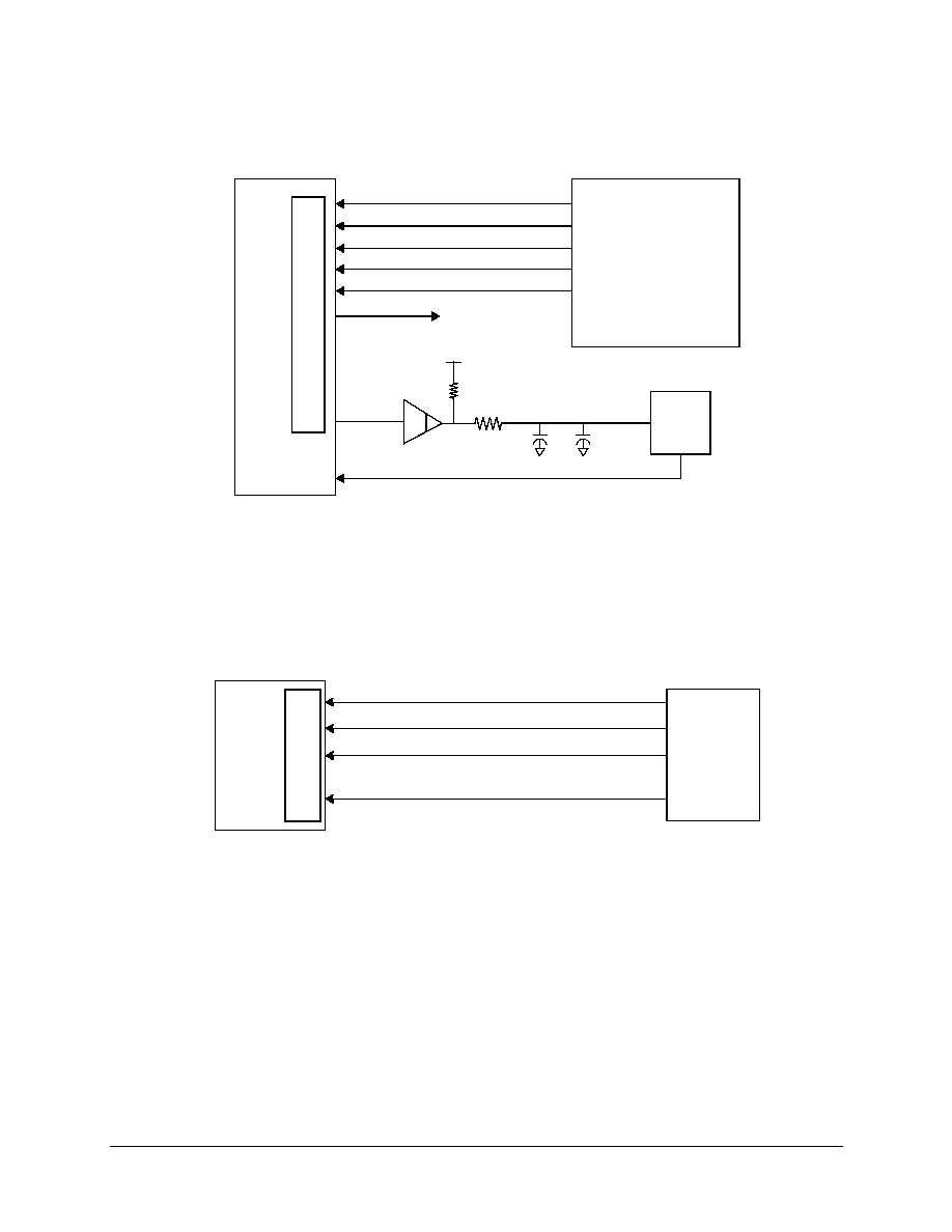
43
September 6, 2002
HWR.BSP15.DS.REV.H
BSP-15 Processor Datasheet
5.4 Transport Channel Interface (TCI)
5.5 NTSC Decoder
SATELLITE/CABLE
SOURCE DECODER
(QAM-QPSK)
&
FORWARD ERROR
CORRECTION
BSP-
15
DSP
VIDEO IN POR
T
0
tcia_clk
tci_data
tcia_enable
tcia_sync
tcia_err#
tcia_inuse
6K
1K
5V
0.01 �F
cer.
1 �F
tant.
O.C.
tcia_vdac
VCXO
27 MHz
pclk
Figure 5.9 Transport Channel
NTSC/PAL
Decoder
pixel_clk
ntsc_ina_hsync
ntsc_ina_vsync
ntsc_ina_data[7:0]
ntsc_ina_clk27
BSP-
15
DSP
V
i
deo
In
P
o
rt
0
Figure 5.10 ITU-R BT.656 NTSC/PAL decoder

44
BSP-15 Processor Datasheet
HWR.BSP15.DS.REV.H
September 6, 2002
5.6 NTSC Encoder
5.7 CRT
ntsc_out_hsync
ntsc_out_vsync
ntsc_out_data[7:0]
pclk
NTSC/PAL
Encoder
VCXO
27 MHz
I
T
U
-
R B
T
.6
01/
6
56 O
u
t
p
ut
BSP-
15
DS
P
Figure 5.11 NTSC/PAL encoder
75
C
C
Z
0
= 75
gdac_green
gdac_blue
gdac_red
vsync
hsync
gdac_comp
V
ref
= 1.235V
L
NOTE:
gdac_blue and gdac_red have the
same connections as those of
gdac_green.
gdac_fscale
R = 1117
Z
l
= 75
BSP-
15
DS
P
AN
ALOG C
R
T I
N
TER
F
A
C
E
Figure 5.12 CRT
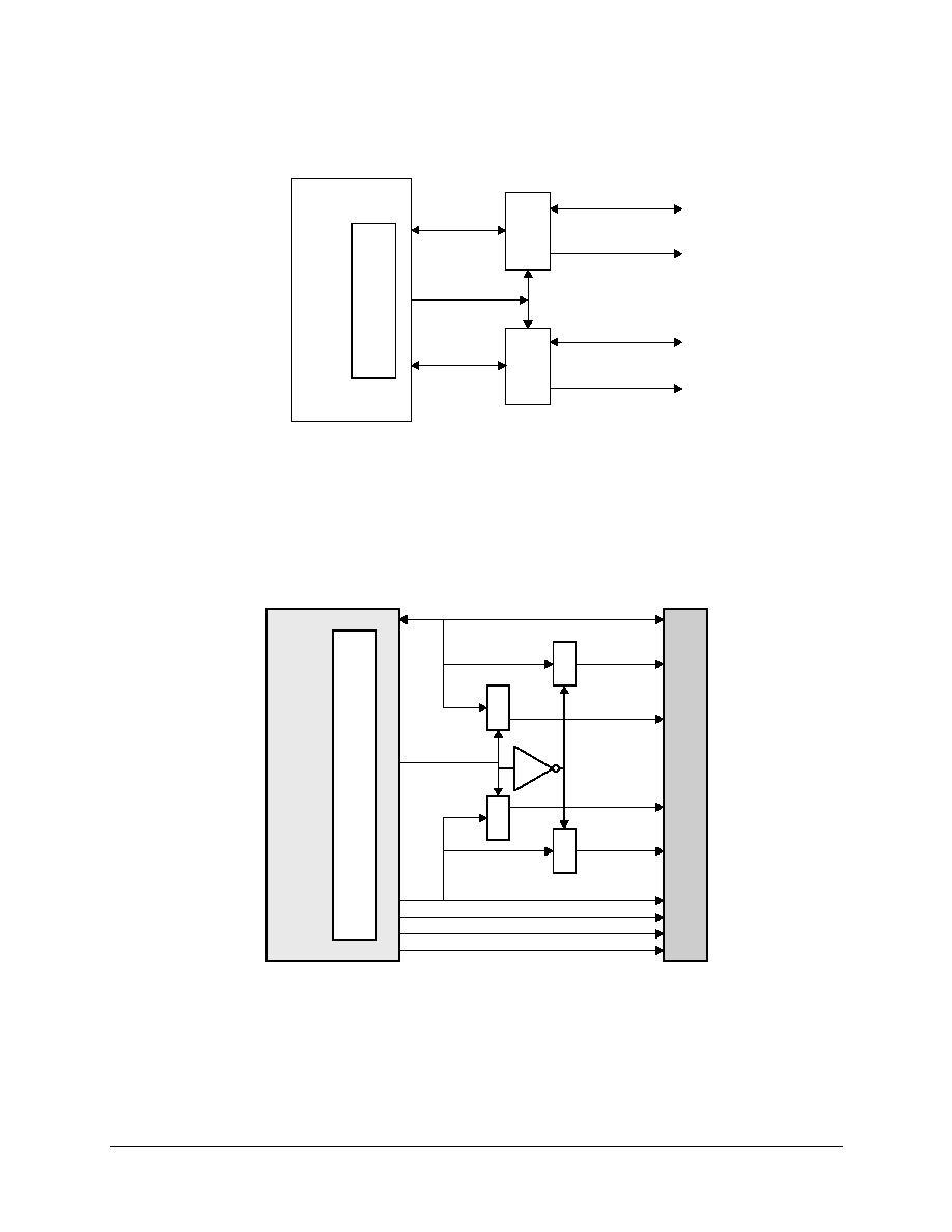
45
September 6, 2002
HWR.BSP15.DS.REV.H
BSP-15 Processor Datasheet
5.8 IIC
5.9 ROM
II
C
BSP-
15
DSP
iic_sda
iic_select
IIC data line
Other data line
IIC clock line
Other clock line
MUX
MUX
iic_sck
Figure 5.13 IIC interface
Figure 5.14 ROM connections
F
L
ASH R
O
M
INTER
F
A
C
E
BSP
-
15
DS
P
FLASH R
O
M
latch
latch
lat
c
h
latch
rom_data[7:0]
addr[9:2]
addr[17:10]
rom_addr[1:0]
addr[21:20]
addr[19:18]
rom_cs_l
rom_wr_l
rom_oe_l
rom_ale

46
BSP-15 Processor Datasheet
HWR.BSP15.DS.REV.H
September 6, 2002

September 6, 2002
HWR.BSP15.DS.REV.H
BSP-15 Processor Datasheet
47
Chapter 6
Electrical Specifications
Note: All electrical specifications are preliminary.
6.1 Absolute Maximum Ratings
Exceeding the maximum values listed in
Table 6-1
may cause permanent damage to the BSP-15 digital
signal processor. This is a stress rating only, and functional operation of the device at these or any other
conditions above those listed in the operational sections of this specification is not implied. Exposure to
absolute maximum rating conditions for extended periods may affect device reliability.
Table 6-1 Absolute Maximum Ratings
Parameter
Max
Unit
Vddcore (measured to Vss)
1.485
V
VddI/O, aVdd_PLL1, aVdd_PLL2, aVddx, aVdd_DAC (measured to Vss)
3.60
V
Voltage on any signal pin
a
,
b
a.
This device employs CMOS devices on all signal pins. It should be handled as an ESD sensitive device.
Voltage on any signal pin that exceeds the power supply voltage by more than +0.5 V can induce destructive
latchup.
b.
PCI Bus pins are 5 V tolerant.
VddI/O + 0.5
V
Storage Temperature
150
�C
Junction Temperature
110
�C
Solder Reflow Temperature
225
�C
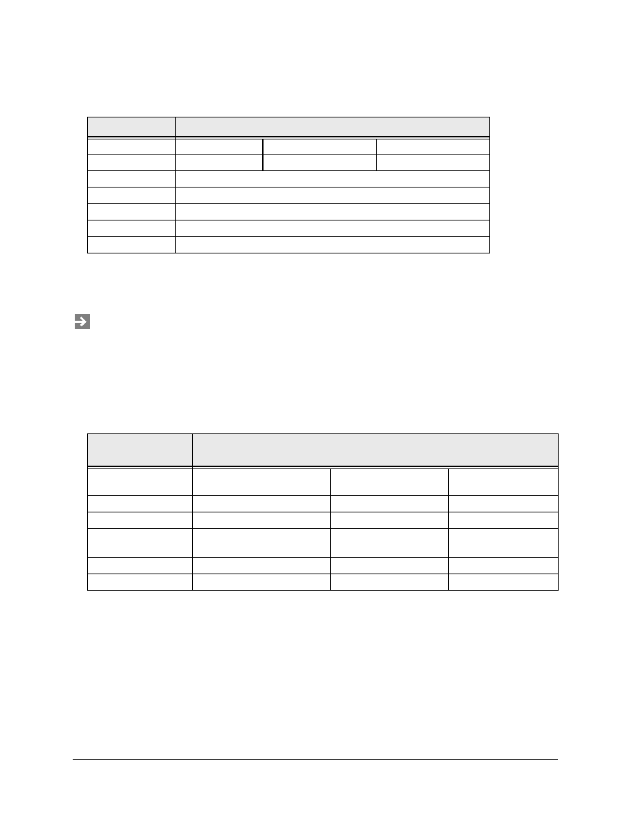
48
BSP-15 Processor Datasheet
HWR.BSP15.DS.REV.H
September 6, 2002
6.2 Power Supply Specifications
The typical estimated total power consumption is 2.5-4.8 W depending on speed, applications, and I/O
loading.
Table 6-2 Voltage Variation
Power Supply
a
a.
Tolerance includes both static and transient variation
Voltage
BSP-15-300
BSP-15-350
BSP-15-400
Vddcore
1.20V
�
5%
1.27V
�
5%
1.35V
�
5%
VddI/O
3.3V
�
5%
aVdd_PLL1
3.3V
�
5%
aVdd_PLL2
3.3V
�
5%
aVdd_DAC
3.3V
�
5%
aVddx
3.3V
�
5%
During power-up, Vddcore must come up before or simultaneously with VddI/O.
VddI/O should not exceed Vddcore by more than 0.4 V while Vddcore is less than 1V.
There is no restriction on the power-down sequence.
The
BSP-15
DSP's PLL supply and both DAC's use 3.3 V.
Table 6-3 Steady State Current
Power
Supply
Estimated Max
Steady State Current
BSP-15-300
(Vddcore 1.2V)
BSP-15-350
(Vddcore 1.27V)
BSP-15-400
(Vddcore 1.35V)
Vddcore
1.6 A
2.2 A
2.9 A
VddI/O
0.25 A
0.25 A
0.25 A
aVdd_PLL1 or
aVdd_PLL2
50 mA
(all 3 PLLs running)
50 mA
50 mA
aVdd_DAC
80 mA
80 mA
80 mA
aVddx
5 mA
5 mA
5 mA
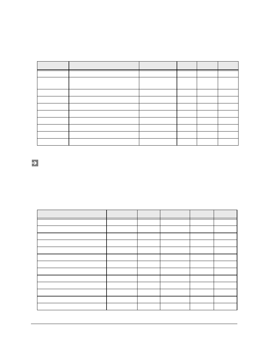
49
September 6, 2002
HWR.BSP15.DS.REV.H
BSP-15 Processor Datasheet
6.3 BSP-15 DC Characteristics
Table 6-4 Input/Output Signals
Parameter
Description
Condition
Min
Max
Unit
V
IL
Input low voltage
-
�0.5
0.6
V
V
IH
Input high voltage
-
2.0
VddI/O +
0.5
V
V
OL
Output low voltage
I
out
= 2 mA
-
0.4
V
V
OH
Output high voltage
I
out
= 2 mA
2.4
-
V
I
LI
Input leakage current
0 < V
in
< VddI/O
�10
10
�A
I
LIPU
Leakage current of pull up pin
0 < V
in
< VddI/O
�300
10
�A
I
LIPD
Leakage current of pull down pin
0 < V
in
< VddI/O
�10
300
�A
I
OZ
Tri-state output leakage
0 < V
in
< VddI/O
�10
10
�A
C
IN
Input pin capacitance
-
-
10
pF
C
IO
Input/output pin capacitance
-
-
12
pF
The relationship between gdac_fscale_f and the full scale output current on IOG is:
IOG (mA) = 24.12
�
gdac_comp(V) / gdac_fscale_f(ohm)
where gdac_comp is 1.235 V (typical).
Table 6-5 Video DAC outputs - aRGB mode
Parameter
Symbol
Min
Typical
Max
Unit
Resolutions (FS)
-
8
8
8
Bits
Integral nonlinearity
INL
-
-
� 2
LSB
Differential nonlinearity
DNL
-
-
�
1
LSB
Monotonicity
-
-
guaranteed
-
-
White level relative to blank
-
17.69
19.05
20.40
mA
White level relative to black
-
16.74
17.62
18.50
mA
Black level relative to blank
-
0.95
1.44
1.90
mA
Blank level on IOG
-
6.29
7.62
8.96
mA
Blank level on IOR, IOB
-
0
5
50
�A
Sync level on IOG
-
0
5
50
�A
LSB size
-
-
69.1
-
�A
DAC-to-DAC matching
-
-
2
5
%
Output resistance
RAOUT
-
37.5
-

50
BSP-15 Processor Datasheet
HWR.BSP15.DS.REV.H
September 6, 2002
6.4 AC Characteristics
The AC timing specifications listed in this section assume a 20 pF load on all output signals of the
BSP-15 DSP.
6.4.1 PLL reference clock input
6.4.2 SDRAM interface timing
Correct setup and hold times can be guaranteed through internal delay adjustment, controlled by bits
[30:24] of the synchronizer/clock control register in the BSP-15 DSP's memory block. The SdMrckDly
and SdMckDly fields control internal delay circuits that affect the timing of signals going to and from
Table 6-6 PLL Reference Clock Input Conditions
Description
Value
Rise/fall time
2 ns maximum (0.4V to 2.4V)
Duty cycle
50% �
�
10%
Maximum cycle to cycle jitter
�
�
200 ps
sdclk, sdclk1, sdclk2
address, data-out, control
sdrtnclk
data-in
t
oh
t
os
t
ds
t
dh
t
sdram
Figure 6.1 SDRAM timing measurement conditions
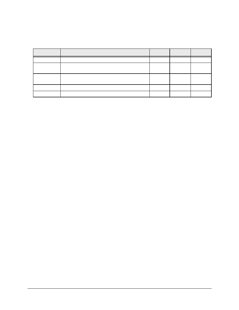
51
September 6, 2002
HWR.BSP15.DS.REV.H
BSP-15 Processor Datasheet
the SDRAM components. They should be adjusted so that setup and hold requirements of both the
SDRAM and the BSP-15 DSP are met.
Table 6-7 SDRAM interface timing parameters
a
a.
Measured with SdMrckDly = 0 and SdMckDly = 3.
Symbol
Description
Min
Max
Unit
f
sdram
b
b.
f
sdram
= 1 / t
sdram
sdclk frequency
-
135
MHz
t
os
Output setup time for address, data, control (sdcs#,
sdras#, sdcas#, sdwe#, sddqm)
1.5
-
ns
t
oh
c
c.
The center of the rising edges of sdclk1 and sdclk2 is used as the reference point.
Output hold time of address, data, control (sdcs_,
sdras_, sdcas_, sdwe_, sddqm)
1.5
-
ns
t
ds
d, e
d.
sdrtnclk is used as the reference clock.
e.
A matching mechanism is provided to compensate for the propagation delay through circuit board traces to
and from the external SDRAM devices. To optimize read timing margin, sdrtnclk should be connected to
sdclk with a dedicated trace, with an optional lumped RC load attached to the middle, to account for the
number of SDRAM devices attached to the clock line.
Input data setup time
2
-
ns
t
dh
c, d
Input data hold time
2
-
ns
52
BSP-15 Processor Datasheet
HWR.BSP15.DS.REV.H
September 6, 2002
6.4.3 PCI bus timing
V
tl
V
th
V
test
t
rval
t
fval
V
trise
t
off
t
on
tri-state
output
output delay
output delay
pci_clk
V
tfall
Figure 6.2 PCI output timing measurement conditions
pci_clk
input
V
th
V
tl
V
test
input valid
t
su
V
test
t
h
V
test
V
max
V
tl
V
th
Figure 6.3 PCI input timing measurement conditions

53
September 6, 2002
HWR.BSP15.DS.REV.H
BSP-15 Processor Datasheet
Table 6-8 PCI interface timing parameters
Symbol
Description
Min
Max
Unit
t
pci_clk
clock cycle time
15
30
ns
t
high
clock high time
6
-
ns
t
low
clock low time
6
-
ns
clk
slew
clock slew rate
1.5
4
V/ns
t
su(bus)
input set up time to clk, bussed signals
3
-
ns
t
su(ptp)
input set up time to clk, point-to-point signals
5
-
ns
t
val(bus)
clk to signal valid delay, bussed signals
2
6
ns
t
val(ptp)
clk to signal valid delay, point to point signal
2
6
ns
t
on
float to active delay
2
-
ns
t
off
active to float delay
-
14
ns
t
h
input hold time from clock
500
-
ps
t
rst
a
a.
pci_rst_ is asserted and de-asserted asynchronously with respect to pci_clk. All output drivers are floated
when pci_rst_ is active.
reset active time after power stable
1
-
ms
t
rst-clk
reset active time after clk stable
100
-
�s
t
rst-off
reset active to output float delay
-
40
ns
Table 6-9 PCI measurement conditions
Symbol
Value
Unit
V
max
0.4 VddI/O
V
V
test
0.4 VddI/O
V
V
tfall
0.615 VddI/O
V
V
th
0.6 VddI/O
V
V
tl
0.2 VddI/O
V
V
trise
0.285 VddI/O
V
Input signal slew rate
1.5
V/ns

54
BSP-15 Processor Datasheet
HWR.BSP15.DS.REV.H
September 6, 2002
6.4.4 IEC958 interface timing
6.4.5 IIS interface timing
The audio PLL generates audioclk_out for use by external codecs as master MCLK. MCLK can be
programmed for either 12.288 MHz or 16.933 MHz to achieve the desired audio sample rate (LRCLK),
according to
Table 6-11
. The MSB:LSB ordering can be reversed by software programming.
Table 6-10 IEC958 interface timing parameters
Symbol
Description
Min
Typical
Max
Unit
F
s
Audio sample rate
32
44.1
48
kHz
n n-1 n-2 n-3
3
2
0
1
L
S
B
M
S
B
n n-1 n-2 n-3
3
2
0
1
L
S
B
M
S
B
Left Channel
Right Channel
One serial bit
clock delay from
LRCLK transmit
4
4
Figure 6.4 IIS data format
55
September 6, 2002
HWR.BSP15.DS.REV.H
BSP-15 Processor Datasheet
Table 6-11 IIS clock ratios
LRCLK
a
(kHz)
MCLK
b
(MHz)
SCLK
c
(MHz)
MCLK/
LRCLK
MCLK/
SCLK
BITS/
FRAME
d
BITS/
CHANNEL
48(TDB)
12.288
1.536
256
8
32
16
44.1
16.933
e
2.116
384
8
48
24
32
12.288
1.536
384
8
48
24
a.
LRCLK = iis_in_lr or iis_out_lr.
b.
MCLK = audioclk_out; MCLK defaults to 27 MHz on power-up (audio PLL bypassed).
c.
SCLK = iis_in_bclk or iis_out_bclk.
d.
Bits/Frame = 2*Bits/Channel = SCLK/LRCLK. When MCLK/LRCLK = 384, 24 bits per channel are always
transmitted, but the number of valid bits is selectable from 16, 18, 20 or 24.
e.
MCLK defaults to 16.933 MHz when audio PLL is enabled.
Table 6-12 IIS output timing parameters
Symbol
Description
Min
Max
Unit
F
s
Output sample rate
32, 44.1, 48
kHz
t
slr
SCLK falling to LRCLK delay
�10
10
ns
t
sdo
SCLK falling to SDATA valid
�10
10
ns
t
slr
t
sdo
iis_out_bclk
iis_out_lr
iis_out_data
Figure 6.5 IIS output timing measurement conditions
56
BSP-15 Processor Datasheet
HWR.BSP15.DS.REV.H
September 6, 2002
Table 6-13 IIS input timing parameters - slave mode
Symbol
Description
Min
Max
Unit
F
s
Input sample rate
32, 44.1, 48
kHz
F
mclk
MCLK frequency
see
Table 6-11
From Table
T
bclk
SCLK period
8/F
mclk
-
From Table
T
low
SCLK pulse width low
2/F
mclk
-
From Table
T
high
SCLK pulse width high
2/F
mclk
-
From Table
t
slrh
SCLK rising to LRCLK hold
20
-
ns
t
slrs
SCLK rising to LRCLK setup
20
-
ns
t
sds
SDATA valid to SCLK rising setup
20
-
ns
t
sdh
SCLK rising to SDATA hold time
20
-
ns
t
slrh
t
slrs
t
low
t
high
t
bclk
t
sds
t
sdh
iis_in_bclk
iis_in_lr
iis_in_data
Figure 6.6 IIS input timing measurement - slave mode
t
sclkr
t
sds
t
sdh
iis_out_bclk
iis_out_lr
iis_in_data
Figure 6.7 IIS input timing measurement - master mode

57
September 6, 2002
HWR.BSP15.DS.REV.H
BSP-15 Processor Datasheet
Table 6-14 IIS input timing parameters - master mode
Symbol
Description
Min
Typical
Max
Unit
F
s
Input sample rate
32
44.1,
48
kHz
F
mclk
MCLK frequency
see
Table 6-11
From Table
T
bclk
SCLK period
8/F
mclk
-
-
From Table
t
sclkr
SCLK rising to LRCLK edge
-
T
bclk
/2
-
�s
t
sds
SDATA valid to SCLK rising setup
(1/F
mclk
)+10 -
-
ns
t
sdh
SCLK rising to SDATA hold
(1/F
mclk
)+15 -
-
ns
internal LRCK
MCLK
internal SCLK
SDATA
N
2
N
N = MCLK / SCLK
Figure 6.8 Internal serial clock generation for IIS master
58
BSP-15 Processor Datasheet
HWR.BSP15.DS.REV.H
September 6, 2002
6.4.6 Transport Channel Interface timing
The timing diagram and
Table 6-15
are relevant to the primary TCI input port. Timing
relationships, input setup, and hold times are identical for the secondary TCI input port.
However, the
tci_vdac
output is not present on the secondary output port. Inputs
video_ina[9:0]
includes
tci_data[7:0]
(bits 7:0),
tci_enable
(bit 8), and
tci_err_
(bit 9)
Table 6-15 TCI timing parameters
Symbol
Description
Min
Max
Unit
f
tci
TCI clock frequency
a,
b,
c,
d
a.
In parallel mode, it is required that t
core
> f
tci_clk
.
b.
In serial mode, it is required that t
core
> � f
tci_clk
.
c.
For correct audio clock counter operation, f
core
/f
audio
> 4, where f
audio
is the frequency of audioclk_out
produced by the on-chip PLL.
d.
For correct video clock counter operation, f
core
/f
video
> 4, where f
video
is the frequency of pclk.
-
27 (parallel)
80 (serial)
MHz
t
h
Hold time
1
-
ns
t
s
Setup time
4
-
ns
tci_clk
tci_sync
t
h
t
s
tci_data
tci_enable
tci_err_
t
tci
Figure 6.9 TCI timing measurement conditions
59
September 6, 2002
HWR.BSP15.DS.REV.H
BSP-15 Processor Datasheet
6.4.7 ITU-R BT.601/656 interface timing
Table 6-16 ITU-R BT.601/656 input interface timing parameters
Symbol
Description
Min
Max
Unit
f
ntsc_in
NTSC input clock frequency
-
MHz
t
h
Input hold time for video_ina[9:0], from cross over of rising
clock
1
-
ns
t
s
Input setup time video_ina[9:0], to the cross over of rising
clock
5
-
ns
This timing diagram and table include information for the primary video input port. The
primary video input bus
video_ina[9:0]
includes the byte-wide data bus (bits 7:0),
horizontal sync (bit 8), and vertical sync (bit 9). The secondary video input signals have
identical timing relationships
t
ntsc_in
ntsc_ina_clk27
ntsc_ina_hsync
ntsc_ina_vsync
ntsc_ina_data[7:0]
t
s
t
h
Figure 6.10 ITU-R BT.601/656 input timing measurement
t
pclk
pclk
t
delay
ntsc_out_data[7:0]
ntsc_out_hsync
ntsc_out_vsync
t
hold
Figure 6.11 ITU-R BT.601/656 output timing measurement
60
BSP-15 Processor Datasheet
HWR.BSP15.DS.REV.H
September 6, 2002
.
6.4.8 General Purpose Data Port
Table 6-17 ITU-R BT.601/656 output interface timing parameters
Symbol
Description
Min
Max
Unit
t
pclk
pclk cycle time
18.5
37 ns
t
delay
Maximum delay time
-
11 ns
t
hold
Output hold time
4
- ns
Table 6-18 GPDP input timing parameters
Symbol
Description
Min
Max
Unit
t
rcv
Receive clock cycle time
-
60
MHz
t
h
Hold time
0
-
ns
t
s
Setup time
4
-
ns
t
rcv
rcv_clk
rcv_data_in[7:0]
rcv_req
xmt_ack
t
s
t
h
Figure 6.12 GPDP input timing measurement conditions
t
xmt
xmt_clk
t
delay
xmt_data_out[7:0]
xmt_req
rcv_ack
t
hold
Figure 6.13 GPDP output timing measurement conditions
61
September 6, 2002
HWR.BSP15.DS.REV.H
BSP-15 Processor Datasheet
6.4.9 IIC interface timing
Table 6-19 GPDP output timing parameters
Symbol
Description
Min
Max
Unit
t
xmt
Transmit clock cycle time
-
60
MHz
t
hold
Output hold time
3.0
-
ns
t
delay
Maximum delay time
-
8
ns
t
f
t
hd_sta
t
low
t
r
Start
t
su_dat
t
f
t
hd_dat
t
high
t
hd_sta
t
su_sta
Stop
t
buf
t
r
t
su_sto
Repeated
Start
iic_sda
iic_sck
Start
Figure 6.14 IIC timing measurement conditions
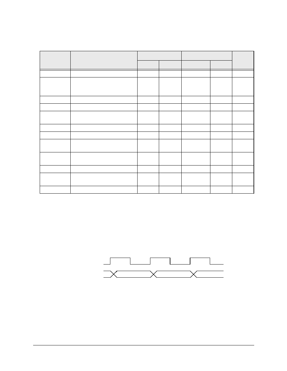
62
BSP-15 Processor Datasheet
HWR.BSP15.DS.REV.H
September 6, 2002
6.4.10 dRGB timing
The BSP-15 generates all dRGB data signals on the rising edge of the
pixelclk_out
clock output.
An external device should latch the dRGB data with the falling edge of
pixelclk_out
.
Table 6-20 IIC interface timing parameters
Symbol
a
a.
All values referred to V
IHmin
and V
ILmax
levels. See
Table 6-4
.
Description
Standard Mode
Fast Mode
Unit
Min
Max
Min
Max
f
sck
iic_sck clock frequency.
0
100
0
400
kHz
t
hd_sta
Hold time (repeated) START
condition. After this period, the
first clock pulse is generated.
2.3
-
0.57
-
�s
t
low
LOW period of the iic_sck clock.
4.7
-
1.27
-
�s
t
high
HIGH period of the iic_sck clock.
4.0
-
0.6
-
�s
t
su_sta
Setup time for a repeated START
condition.
4.7
-
0.6
-
�s
t
hd_dat
Data hold time.
0
b
b.
A device must internally provide a hold time of at least 300 ns for the SDA signal (referred to the V
IHmin
of
the SCL signal) to bridge the undefined region of the falling edge of SCL.
3.45
0
b
0.9
�s
t
su_dat
Data setup time.
250
-
250
-
ns
t
r
Rise time of both iic_sda and
iic_sck signals.
-
1000
20 + 0.1C
b
c
c.
C
b
= total capacitance of one bus line in pF.
300
ns
t
f
Fall time of both iic_sda and
iic_sck signals.
-
300
20 + 0.1C
b
300
ns
t
su_sto
Setup time for STOP condition.
4.0
-
0.6
-
�s
t
buf
Bus free time between a STOP
and START condition.
4.7
-
1.3
-
�s
C
b
Capacitive load for each bus line.
-
400
-
400
pF
dRGB(n)
dRGB(n + 1)
dRGB(n + 2)
dRGB(23:0)
pixelclk_out
Figure 6.15 dRGB timing diagram

63
September 6, 2002
HWR.BSP15.DS.REV.H
BSP-15 Processor Datasheet
6.5 Termination Characteristics
6.5.1 Basic rules
This document specifies the proper termination for the BSP-15 DSP pins when specific blocks are not
used. The basic rules are: float output pins; tie unused inputs to inactive level; special terminations are
otherwise indicated.
6.5.1.1 Weak pull down and pull up defined
The manufacturer assumes the use of a terminate with a 10 to 20 k
resistor for weakly pulling up or
pulling down a pin.

64
BSP-15 Processor Datasheet
HWR.BSP15.DS.REV.H
September 6, 2002
6.5.2 Processor clock
6.5.3 ROMCON
ROM shares I/O with other interfaces during normal operational mode.
Table 6-21 Processor Clock Terminations
Pin Name
Termination
Notes
pclk
see notes
supplies reference clock for the on-chip CORE/SDRAM, AUDIO, and
PIXEL PLLs.
coreclk_byp_in
see notes
CORE PLL uses this signal when the PLL is programmed to be in the
bypass mode. It supplies the clock for the VLIW core. The CORE PLL
comes out of reset in bypass mode, the bypass clock is needed during the
booting phase, a clock input to this pin is ESSENTIAL. The manufacturer
recommends tying the coreclk_byp_in and pclk together.
sdclk_byp_in
see notes
SDRAM PLL uses this signal when the PLL is programed to be in the
bypass mode. It supplies the clock for the SDRAM interface. If the
application will not use bypass mode, feed a slow frequency clock since this
signal is used during the memory block reset phase (i.e., the chip reset
phase), for some internal registers to be reset correctly. The clock needs to
be fast enough to produce a couple of edges during the time when the chip
is in reset.
pixelclk_byp_in see notes
PIXEL PLL uses the signal when the PIXEL PLL is programmed to be in
the bypass mode. It supplies the pixel clock for DRC and VideoDAC.
When not used, it can be weakly pulled down to ground. In BSP-15 DSP,
this signal can also be optionally used for the ITU-R.BT 656_OUT block,
as the output clock for the 8-bit parallel data port.
audioclk_byp_in see notes
AUDIO PLL uses the signal when the AUDIO PLL is programmed to be in
the bypass mode. It supplies the clock for the audio blocks. When not
used, it can be weakly pulled down to ground.
coreclk_out
see notes
This is the output of the core clock from the CORE PLL, used for debug.
When not used, it can be left floating.
pixelclk_out
see notes
This is the output of the pixel clock from the PIXEL PLL, used for debug.
Leave floating when not used.
audioclk_out
see notes
This is the output of the audio clock from the AUDIO PLL, used for debug.
Leave floating when not used.
Table 6-22 ROMCOM Terminations
Pin Name
Termination
Notes
rom_ale#
floating
rom_wrt
floating
rom_oe#
floating
rom_cs#
floating
65
September 6, 2002
HWR.BSP15.DS.REV.H
BSP-15 Processor Datasheet
6.5.4 PCI
Versaport [22] should also have a weak pull-up to Vdd
Table 6-23 PCI Termination
Pin Name
Termination
Notes
pci_ad[31..0
float
pci_cbe[3..0]
float
pci_frame#
weak pull up to Vdd
pci_trdy#
weak pull up to Vdd
pci_irdy#
weak pull up to Vdd
pci_stop#
weak pull up to Vdd
pci_par
float
pci_devsel#
weak pull up to Vdd
pci_clk
connect to low frequency clk signal
pci_rst#
chip reset
pci_inta#
weak pull up to Vdd
pci_req[0]#
weak pull up to Vdd
pci_gnt[0]#
weak pull up to Vdd
pci_req[1]
weak pull up to Vdd
pci_gnt[1]#
weak pull up to Vdd
pci_req[2]
weak pull up to Vdd
pci_gnt[2]#
weak pull up to Vdd
pci_serr_intb#
weak pull up to Vdd
pci_idsel#
weak pull up to Vdd
pci_pme#
weak pull up to Vdd

66
BSP-15 Processor Datasheet
HWR.BSP15.DS.REV.H
September 6, 2002
6.5.5 ITU-R BT.601/656 out
6.5.6 Video input ports
6.5.6.1 TCIA
Table 6-24 ITU-R BT.601/656 Out Termination
Pin Name
Termination
Notes
tcia_vdac
float
ntsc_clk27_vcxo
�
shared with pclk
ntsc_out_hsync
float
ntsc_out_vsync
float
ntsc_out_data[7]
see notes
sw_strap (input, 4 pins): ...... Software straps for boot. These
signal are also multiplexed with
rom_data[7..4].
These straps may be used in any way desired. The manufacturer uses
these straps to indicated to the software the type of board is in use.
ntsc_out_data[6]
see notes
ntsc_out_data[5]
see notes
ntsc_out_data[4]
see notes
ntsc_out_data[3]
float
ntsc_out_data[2]
float
ntsc_out_data[1]
see notes
pci_host
(input,
1
pin): ........ BSP-15 DSP is host on the
primary PCI bus. This signal is
multiplexed with rom_data[1].
When the BSP-15 DSP is the pci host, this pin should be weakly
pulled up with a 4.7k
resistor. When the BSP-15 DSP is not the pci
host, this pin should be weakly pulled down with a 4.7k
resistor.
ntsc_out_data[0]
see notes
rom_boot (input, 1 pin): ...... Flash rom used for boot. This
signal is multiplexed with
rom_data[0].
When ROM boot is used, this pin should be weakly pulled up with a
4.7k
resistor. When PCI boot is used, this pin should be weakly
pulled down with a 4.7k
resistor.
Table 6-25 TCIA Terminations
Pin Name
Termination
Notes
tcia_data[7..0] / video_ina[7..0]
weakly pull down
tcia_enable / video_ina[8]
weakly pull down
tcia_sync
weakly pull down
tcia_err# / video_ina[9]
weakly pull down
tcia_clk
weakly pull down
tcia_inuse
float
tcia_vdac
float
The pin is the simulated sigma delta output that
controls the software PLL loop that tracks the
transport encoder video clock. The pin is shared by
the TCIA and TCIB block.
67
September 6, 2002
HWR.BSP15.DS.REV.H
BSP-15 Processor Datasheet
6.5.6.2 TCIB
6.5.7 ITU-R BT.601/656 IN_A
6.5.8 ITU-R BT.601/656 IN_B
6.5.9 IIS
Table 6-26 TCIA Terminations
Pin Name
Termination
Notes
tcib_data[7..0] / video_ina[7..0]
weakly pull down
tcib_enable / video_ina[8]
weakly pull down
tcib_sync
weakly pull down
tcib_err# / video_ina[9]
weakly pull down
tcib_clk
weakly pull down
tcib_inuse
float
tcib_vdac
float
See tcia_vdac above.
Table 6-27 ITU-R BT.601/656 IN_A Terminations
Pin Name
Termination
Notes
ntsc_ina_data[7..0] / video_ina[7..0]
weakly pull down
ntsc_ina_hsync / video_ina[8]
weakly pull down
ntsc_ina_vsync / video_ina[9]
weakly pull down
ntsc_ina_clk27
weakly pull down
Table 6-28 ITU-R BT.601/656 IN_B Terminations
Pin Name
Termination
Notes
ntsc_inb_data[7..0] / video_inb[7..0]
weakly pull down
ntsc_inb_hsync / video_inb[8]
weakly pull down
ntsc_inb_vsync / video_inb[9]
weakly pull down
ntsc_inb_clk27
weakly pull down
Table 6-29 IIS Terminations
Pin Name
Termination
Notes
iis_in_data
weakly pull down
iis_in_lr
weakly pull down
iis_in_bclk
weakly pull down
iis_out_data[2..0]
float
iis_out_mclk / audioclk_out
float
iis_out_lr
float
iis_out_bclk
float
68
BSP-15 Processor Datasheet
HWR.BSP15.DS.REV.H
September 6, 2002
6.5.10 IEC958
6.5.11 IIC/DDC
6.5.12 JTAG
6.5.13 DRC / VideoDAC
Table 6-30 IEC 958 Terminations
Pin Name
Termination
Notes
iec958_out
float
iec958_in
weakly pull down
Table 6-31 IIC/DDC Terminations
Pin Name
Termination
Notes
iic_sda
weakly pull down
iic_sck
weakly pull down
ddc_select
float
Table 6-32 JTAG Terminations
Pin Name
Termination
Notes
tck
weakly pull down
tms
weakly pull down
tdi
weakly pull down
trst
weakly pull down
tdo
float
Table 6-33 DRC / VideoDAC
Pin Name
Termination
Notes
vsync
float
hsync
float
gdac_comp
Vref, weakly pull down
gdac_fscale
tie to ground
gdac_green
weakly pull up to VddI/O
gdac_blue
weakly pull up to VddI/O
gdac_red
weakly pull up to VddI/O
aVdd_DAC (D16)
tie to VddI/O
no extra filter needed
aVddx (D17)
tie to VddI/O
no extra filter needed
aVss (A17)
tie to ground Vss

69
September 6, 2002
HWR.BSP15.DS.REV.H
BSP-15 Processor Datasheet
A PIO bit in the DRC controls the VideoDAC powerdown
aVssx (B19)
tie to ground Vss
gdac_cvgg (C18)
tie to ground Vss
Table 6-33 DRC / VideoDAC
Pin Name
Termination
Notes

70
BSP-15 Processor Datasheet
HWR.BSP15.DS.REV.H
September 6, 2002
September 6, 2002
HWR.BSP15.DS.REV.H
BSP-15 Processor Datasheet
71
Chapter 7
Thermal Specifications
Thermal parameters are shown in
Table 7-1
. Note that
JA
can be improved by providing either passive or active
cooling.
Table 7-1 Thermal Parameters
Symbol
Parameter
Min
Max
Unit
C
Operating Case Temperature
a
a.
Measured at top center of case surface with the device soldered to circuit board
0
85
�C
J
Operating Junction Temperature
105
�C
JA
Thermal Resistance Junction to Ambient
b
b.
Values are for 0 [ft/min] airflow
11.4
�C/W

72
BSP-15 Processor Datasheet
HWR.BSP15.DS.REV.H
September 6, 2002
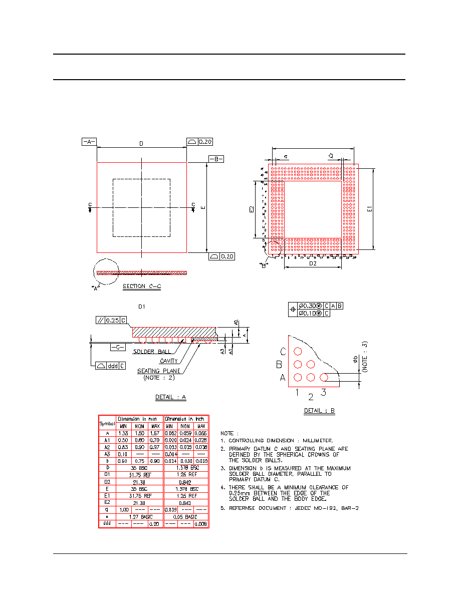
September 6, 2002
HWR.BSP15.DS.REV.H
BSP-15 Processor Datasheet
73
Chapter 8
Mechanical Specifications
8.1 EBGA352 Package
Figure 8.1 EBGA352 Package
74
BSP-15 Processor Datasheet
HWR.BSP15.DS.REV.H
September 6, 2002
8.2 Package Materials
.
Table 8-1 Materials specification
Segment
Material
Package substrate
BT Resin
Encapsulation
Epoxy with filler
Heat Spreader
Cu + Ni plating
Solder Ball
37 Pb - 63 Sn
The package shown here is the MAP-CA DSP pin-compatible package. Other packaging
options are available. Please contact Equator Technologies, Inc. sales representatives for
details.

September 6, 2002
HWR.BSP15.DS.REV.H
BSP-15 Processor Datasheet
75
Appendix A
Glossary
These acronyms and names used in this Data Sheet. These are their expansion or explanation.
aRGB ........................................ analog RGB
BSDL ........................................ Boundary Scan Description Language
DataStreamer DMA controller ... High speed DMA controller that operates independent from
VLIW core, also referred to as the DS DMA controller
DRC .......................................... Display Refresh Controller
dRGB ........................................ digital RGB
DS DMA controller ................... the DataStreamer DMA controller
DTS ........................................... Data Transfer Switch - high speed BSP-15 series internal data
bus
FEC ........................................... Forward error correction
I-ALU ....................................... Integer ALU (Arithmetic Logic Unit) - performs loads, stores,
branches, integer arithmetic, and logical operations
IG-ALU ..................................... Integer, Graphics unit - performs integer arithmetic and
(partitioned) multimedia operations
MMU......................................... Memory Management Unit
PLC ........................................... 128-bit Partitioned Local Constant register
PLV ........................................... 128-bit Partitioned Local Variable register
SIMD ........................................ Single Instruction Multiple Data
TLB ........................................... Translation Lookaside Buffer
VLx ........................................... A coprocessor that can accelerate variable length encoding and
variable length decoding.

76
BSP-15 Processor Datasheet
HWR.BSP15.DS.REV.H
September 6, 2002