
Bolymin, Inc.
Bolymin, Inc.
Bolymin, Inc.
Bolymin, Inc.
xxx
LCD MODULE SPECIFICATION
MODEL NO.
BR320240ACNCH
FOR MESSRS:
________________________________________________
ON DATE OF:
________________________________________________
APPROVED BY:
________________________________________________

Bolymin, Inc.
Bolymin, Inc.
Bolymin, Inc.
Bolymin, Inc.
xxx
C O N T E N T S
1. Numbering System
2. LCD Module Handling Precautions
3. General Specification
4. Absolute Maximum Ratings
5. Electrical Characteristics
6. Optical Characteristics
7. Interface Description
8. Block diagram
9. Timing Characteristics
10. Power supply for LCD Module and LCD operating voltage adjustment
11. Backlight information
12. Display Pattern
13. Quality Assurance
14. Reliability
Bolymin, Inc.
Bolymin, Inc.
Bolymin, Inc.
Bolymin, Inc.
xxx
1. . . .
Numbering System
B C 2004
A
G
P
L
E
B
xxx
0
1
2
3
4
5
6
7
8
9
0
Brand
Bolymin
1
Module
Type
C= character type
G= graphic type
P= TAB/TCP type
O= COG type
F= COF type
2
Format
2002=20 characters, 4
lines
12232= 122 x 32 dots
3
Version
No.
A type
4
LCD Color
G=STN/gray
Y=STN/yellow-green
C=color STN
B=STN/blue
F=FSTN
T=TN
5
LCD Type
R=positive/reflective
P=positive/transflective
M=positive/transmissi
ve
N=negative/transmissi
ve
6
Backlight
type/color
L=LED array/
yellow-green
H=LED edge/white
R=LED array/red
G=LED
edge/yellow-green
D=LED edge/blue
E=EL/white
B=EL/blue
C=CCFL/white
7
CGRAM
Font
J=English/Japanese
Font
E=English/European
Font
C=English/Cyrillic
Font
H=English/Hebrew
Font
8
View
Angle/
Operating
Temperat
ure
B=Bottom/Normal
Temperature
H=Bottom/Wide
Temperature
U=Bottom/Ultra wide
Temperature
T=Top/Normal
Temperature
W=Top/Wide
Temperature
C=9H/Normal
Temperature
9
Special
Code
3=3 volt logic power
supply
n=negative voltage for
LCD
c=cable/connector
xxx=to be assigned on
data sheet
t=temperature
compensation for
LCD
p=touch panel

Bolymin, Inc.
Bolymin, Inc.
Bolymin, Inc.
Bolymin, Inc.
xxx
2. LCD Module Handling Precautions
(1)Avoid applying excessive shocks to the module or making any alterations or modifications to it.
(2)Don't make extra holes on the printed circuit board, modify its shape or change the components of
LCD Module.
(3)Don't disassemble the LCM.
(4)Don't operate it above the absolute maximum rating.
(5)Don't drop, bend or twist LCM.
(6)Soldering: only to the I/O terminals.
(7)Storage: please storage in anti-static electricity container and clean environment.
3. General Specification
(1) Mechanical Dimension
ITEM STANDARD
VALUE UNIT
Number of dots
320RGB x240
dots
Outline dimension
154.6(W)x 114.8(H)x 8.5max(T)
mm
View area
118.18(W)x 89.33(H)
mm
Active area
115.18(W)x 86.33(H)
mm
Dot Size
0.09 x RGB x 0.33
mm
Dot Pitch
0.12 x RGB x 0.36
mm
LCD type
Color STN, transmissive
View direction
6 o'clock
Backlight CCFL
Temperature Extended
Range
(2) Controller IC: SED1375
(3) Temperature Range
Normal Wide
Operating
0 ~+50
-20 ~ +70
Storage
-10 ~ +60
-30 ~ +80

Bolymin, Inc.
Bolymin, Inc.
Bolymin, Inc.
Bolymin, Inc.
xxx
4. Absolute Maximum Ratings
ITEM SYMBOL
MIN.
TYP.
MAX.
UNIT
Operating Temperature
T
OP
-20
+70
Storage Temperature
T
ST
-30
+80
Input Voltage
V
I
-0.3
V
dd
V
Supply Voltage For Logic
V
DD
-V
SS
0
6.5 V
Supply Voltage For LCD
V
LCD
-V
SS
0
30 V
5. Electrical Characteristics
ITEM SYMBOL
CONDITION
MIN.
TYP.
MAX.
UNIT
Logic Voltage
V
DD
-V
SS
4.75 5.0 5.25 V
Supply Voltage For LCD
V
LCD
-V
SS
Ta=-20
Ta=25
Ta=70
26.2
V
V
V
Input High Volt.
V
IH
0.8V
DD
V
DD
V
Input Low Volt.
V
IL
0
0.2V
DD
V
Output High Volt.
V
OH
V
DD
-0.4
V
Output Low Volt.
V
OL
0.4 V
Supply Current
I
LCD
7.5
11.0
mA

Bolymin, Inc.
Bolymin, Inc.
Bolymin, Inc.
Bolymin, Inc.
xxx
6. Optical Characteristics
ITEM SYMBAL
CONDITION
MIN TYP MAX UNIT
(V) CR10
10
105 deg.
View Angle
(H) CR10
-30
30 deg.
Contrast Ratio
CR
29.1
T rise
120
ms
Response Time
T fall
252
ms
6.1 Definitions
View Angles
Contrast Ratio
Y
X
( Visual angle direction )
Z
Brightness at non-selected state ( Bns )
Brightness at selected state ( BS )
Non-selected state
Operating voltage for LCD driving
CR =
Selected state
B
r
i
g
h
t
n
e
s
s
(
%
)
Bns
Bs
Bolymin, Inc.
Bolymin, Inc.
Bolymin, Inc.
Bolymin, Inc.
xxx
Response time
1
0
0
%
90 %
Rise Time
Decay Time ( fall time tf )
B
r
i
g
h
t
n
e
s
s
Selected Condition
Nonselected Condition
Nonselected Condition
tr
td
10 %

Bolymin, Inc.
Bolymin, Inc.
Bolymin, Inc.
Bolymin, Inc.
xxx
7. Interface Description
Pin No.
Symbol
Level
Description
1 FRM H
SCAN
START-UPSINGAL
2
CL1
H to L Data latch pulse
3
CL2
H to L Data shift pulse
4
DISP
H/L
H: Display ON, L: Display OFF
5 V
DD
5.0V
Power supply for Logic
6 V
SS
0V
Ground
7 V
LCD
(Variable) Driving voltage for LCD
8 D7 H/L
Display
data
9 D6 H/L
Display
data
10 D5 H/L
Display
data
11 D4 H/L
Display
data
12 D3 H/L
Display
data
13 D2 H/L
Display
data
14 D1 H/L
Display
data
15 D0 H/L
Display
data
Recommendation LCD Connector: MOLEX53261-1510
Bolymin, Inc.
Bolymin, Inc.
Bolymin, Inc.
Bolymin, Inc.
xxx
8. Block diagram
3 2 0 2 4 0 R G B x 2 4 0
D O T S
L C D P A N E L
C O M 1
C O M 2 4 0
S
E
G
1
S
E
G
3
2
0
S E G D r i v e
C
O
M
D
r
i
v
e
r
B I A S
C i r c u i t
M
M
C L 1
C L 1 , C L 2 , M , D I S P
D 0 ~ D 7
C L 1 , F L M
D I S P , M
C C F L B A C K L I G H T
2 L O A D
3 C P
4 D I S P
5 V D D
6 V S S
7 V L C D
8 D 7
D A T A B U S
D 0 ~ D 7
1 F R M

Bolymin, Inc.
Bolymin, Inc.
Bolymin, Inc.
Bolymin, Inc.
xxx
Bolymin, Inc.
Bolymin, Inc.
Bolymin, Inc.
Bolymin, Inc.
xxx
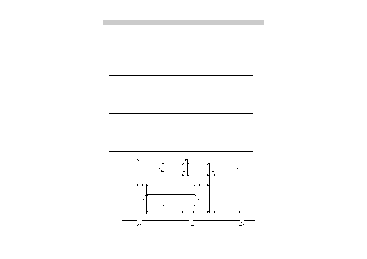
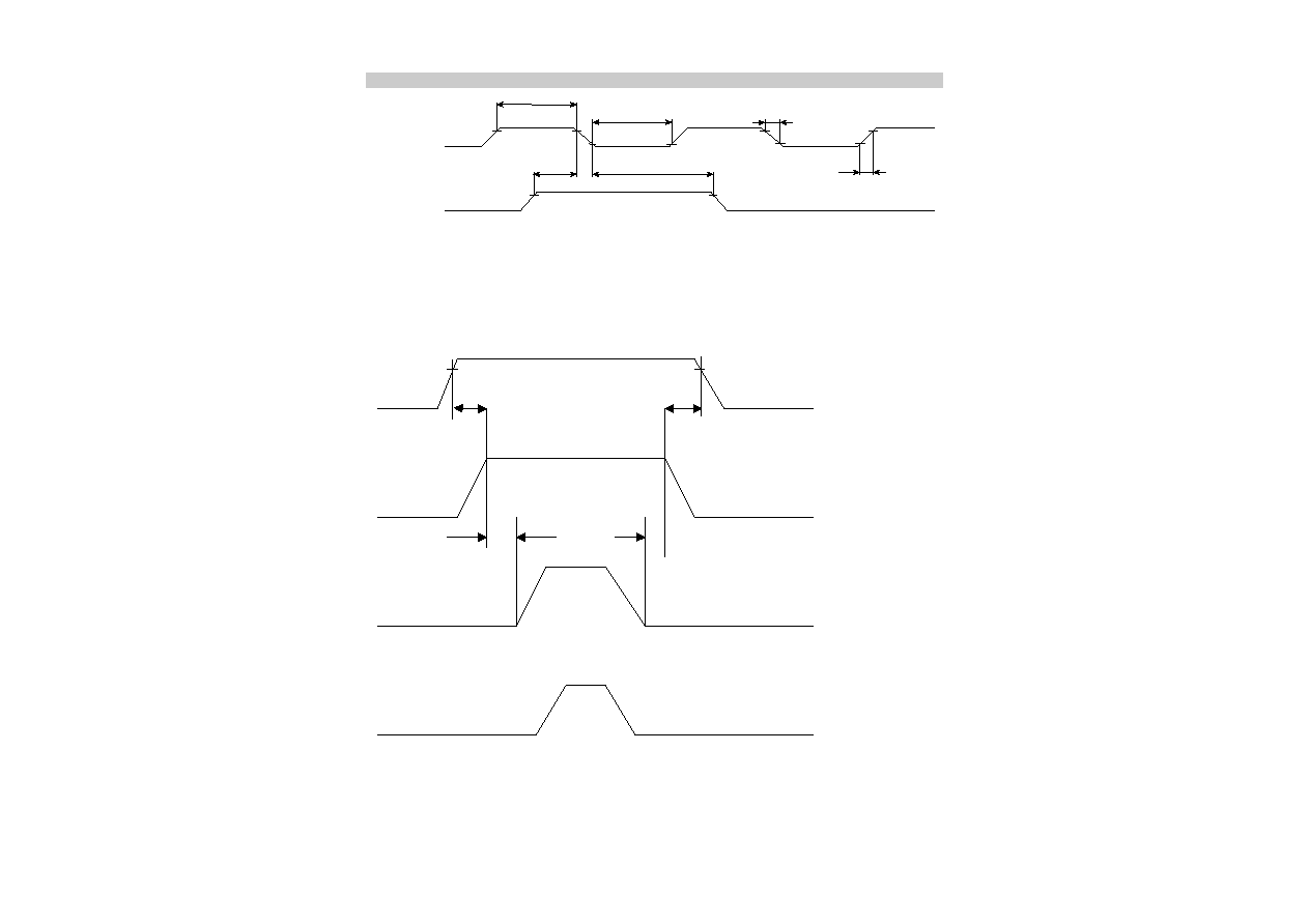
9. Timing Characteristics
9.1.Common & Segment interface timing:
ITEM symbol
Test
Condition Min.
Typ.
Max.
Units
Clock Cycle
tC
Fig.1
500
ns
CP Pulse Width
tWC
Fig.1
240
ns
LP Pulse Width
tWL
Fig.1
240
ns
Data Set Up Time
tDSU
Fig.1
240
ns
Data Hold Time
tDHD
Fig.1
240
ns
CP Rise/Fall Time
tr,tf
Fig.1
50 ns
CP to LOAD
tCL
Fig.1
240
ns
LOAD to CP
tLC
Fig.1
240
ns
LP Pulse Width
tLW
Fig.1
240
ns
CL1 Pulse Width
tCW Fig.2
170
ns
Data Set Up Time
tDSU2
Fig.2
240
ns
Data Hold Time
tDHD2
Fig.2
170
ns
CL1 Rise/Fall Time tr2,tf2
Fig.2
50 ns
CL2(LP)
CL1(CP)
D0~D3
tWC
tWC
tr
tf
tLS
tWL
tSL
tCL
tLC
tDSU
tDHD
80%
20%
Fig 1. SEGMENT TIMING
Bolymin, Inc.
Bolymin, Inc.
Bolymin, Inc.
Bolymin, Inc.
xxx
CL1
FLM
tCW
tCW
tDSU2
TDHD2
tf2
tr2
80%
20%
Fig 2 COMMON TIMING
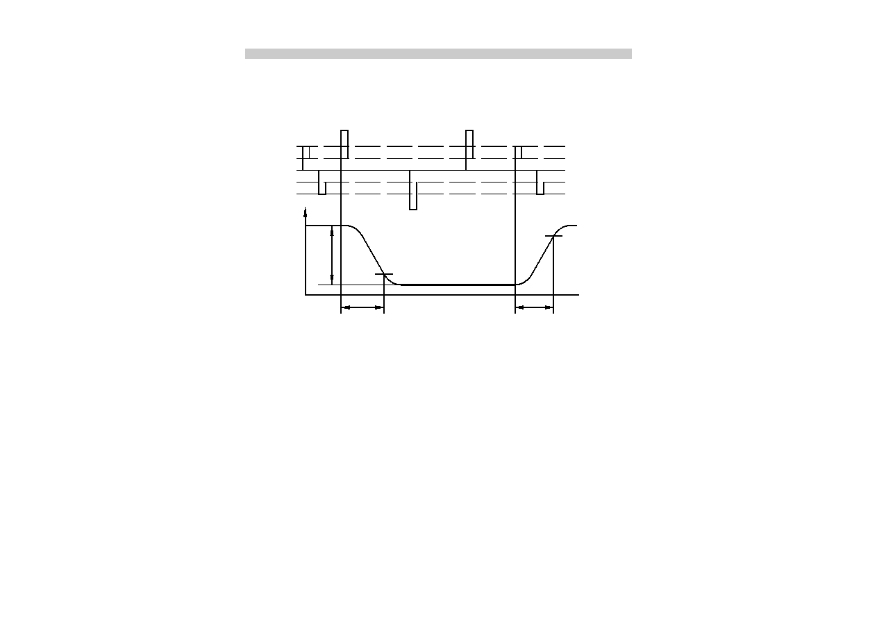
9.2 POWER ON/OFF TIMING
POWER ON POWER OFF
The missing pixels may occur when the LCM is driven beyond above power interface timing sequence.
0.8VD
VSS
VSS
VSS VSS
VSS
VSS
VSS
VSS
0.8VD
VDD
DISP
VLCD
VSS
0ms
20ms min
0~50ms 0~50ms
Bolymin, Inc.
Bolymin, Inc.
Bolymin, Inc.
Bolymin, Inc.
xxx
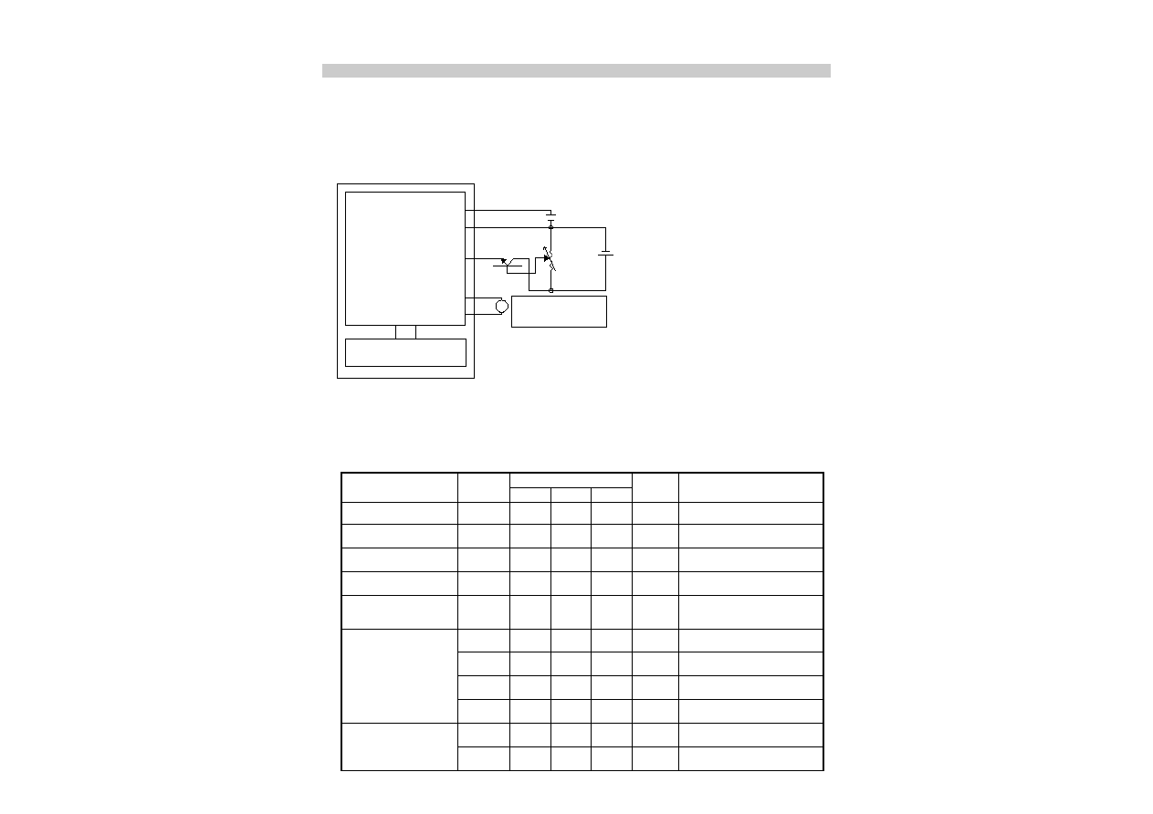
10. Power Supply
PCB
VDD
VSS
Vlcd
VH
GND
CCFL B/L
VR=
10~20K
+30V
+5V
Recommendation
Circuit
11. CCFL Backlight Specification
(Ta=25)
Specification
Item Symbol
Min Typ Max
Unit Condition
Driving Voltage
V
FL
500
Vrms
Input current
I
FL
4.5 5.0 5.5
mArms
Power consumption
W
2.5
W
Starting Voltage
V
FLS
630
Vrms
Luminance L
550
Cd/m
2
,=0 deg, I
FL
=5.0mArms
135
Cd/m
2
White (CCFL B/L)
35
Cd/m
2
Red (CCFL B/L)
45
Cd/m
2
Green (CCFL B/L)
Brightness
35 Cd/m
2
Blue (CCFL B/L)
x
0.340
Chromaticity
y
0.370

Bolymin, Inc.
Bolymin, Inc.
Bolymin, Inc.
Bolymin, Inc.
xxx
Luminance Uniformity
(Testing 9 point)
75%
%
,=0 deg, I
FL
=5.0mArms
Life time
20000
hrs
Recommendation CCFL Connector: BHR-03VS-1(JST)

Bolymin, Inc.
Bolymin, Inc.
Bolymin, Inc.
Bolymin, Inc.
xxx
12. Display Pattern
R
D7
G
D6
B
D5
D3
D4
R G
D2
B
D6
D7
R G
D2
D4 D3
D5
B
R
B
G
D4
D5
D5 D4
G
R
R G
D0
D1
D2
D3
D0
B
D1
D2
D3
R
B
G
B
R
B
G
D0
D0
B
B
D6
D7
D7 D6
G
R
R G
D5 D4 D3 D2 D1
D2
D3
D4
D5
D2
B
D3
D4
D5
R
B
G
D3
D5 D4
R G
D2 D1
R
B
G
B
R
B
G
R G
R
B
G
320 x 3(RGB)
x 320 dot
segment
c
o
m
m
o
n
Bolymin, Inc.
Bolymin, Inc.
Bolymin, Inc.
Bolymin, Inc.
xxx
13. Quality Assurance
Screen Cosmetic Criteria
No. Defect
Judgement
Criterion
Partition
1 Spots
A)Clear
Size: d mm Acceptable Qty in active area
d 0.1 Disregard
0.1<d0.2 6
0.2<d0.3 2
0.3<d 0
Note: Including pin holes and defective dots which
must be within one pixel size.
B)Unclear
Size: d mm Acceptable Qty in active area
d 0.2 Disregard
0.2<d0.5 6
0.5<d0.7 2
0.7<d 0
Minor
2
Bubbles in Polarize
Size: d mm Acceptable Qty in active area
d0.3 Disregard
0.3<d1.0 3
1.0<d1.5 1
1.5<d 0
Minor
3 Scratch
In accordance with spots cosmetic criteria. When the
light reflects on the panel surface, the scratches are not
to be remarkable.
Minor
4 Allowable
Density
Above defects should be separated more than 30mm
each other.
Minor
5 Coloration
Not to be noticeable coloration in the viewing area of
the LCD panels.
Back-light type should be judged with back-light on
state only.
Minor

Bolymin, Inc.
Bolymin, Inc.
Bolymin, Inc.
Bolymin, Inc.
xxx
14. Reliability
Content of Reliability Test
Environmental Test
No.
Test Item
Content of Test
Test Condition
Applicable
Standard
1
High Temperature
storage
Endurance test applying the high
storage temperature for a long time.
70
120hrs
----
2
Low Temperature
storage
Endurance test applying the high
storage temperature for a long time.
-20
120hrs
----
3
High Temperature
Operation
Endurance test applying the electric
stress (Voltage & Current) and the
thermal stress to the element for a
long time.
70
120hrs
----
4
Low Temperature
Operation
Endurance test applying the electric
stress under low temperature for a
long time.
-20
120hrs
----
5
High Temperature/
Humidity Storage
Endurance test applying the high
temperature and high humidity
storage for a long time.
70,90%RH
96hrs
----
6
High Temperature/
Humidity Operation
Endurance test applying the electric
stress (Voltage & Current) and
temperature / humidity stress to the
element for a long time.
70,90%RH
96hrs
----
7
Temperature Cycle
Endurance test applying the low and
high temperature cycle.
-20 25 70
30min 5min 30min
1 cycle
-20/70
10 cycles
----
Mechanical Test
8 Vibration
test
Endurance test applying the vibration
during transportation and using.
10~22Hz1.5mmp-p
22~500Hz1.5G
Total 0.5hrs
----
9 Shock
test
Constructional and mechanical
endurance test applying the shock
during transportation.
50G Half sign
wave 11 msedc
3 times of each direction
----
10
Atmospheric
pressure test
Endurance test applying the
atmospheric pressure during
transportation by air.
115mbar
40hrs
----
Others
11
Static electricity test
Endurance test applying the electric
stress to the terminal.
VS=800V,RS=1.5 k
CS=100pF
1 time
----
***Supply voltage for logic system=5V. Supply voltage for LCD system =Operating voltage at 25
