
1
Atelic
Systems,
Inc.
AT1004 Application Note
Preliminary
4-Channel, ADPCM Processor with Echo Cancellation and Conferencing
Description
The AT1004 is a four full-duplex channel, ADPCM processor with conferencing and echo cancellation capabilities. It
follows the G.726 ITU Standard for ADPCM compression for 40k, 32k, 24k and 16k bitrates with selectable
µ
-law and A-
law input/output. Using the command serial interface, each individual half-channel can be independently configured for
ADPCM, conferencing and echo canceling features. The adaptive line-echo canceling cancels up to 2 ms and converges
within .5 seconds.
Features
·
ITU-T G.726 Standard, 4 full channels / 8 half channels
· µ
-Law and A-law PCM compatible
·
On-chip time slot assignment
·
Available internal clock generator and frame sync. generator
·
Simple 3-wire serial command port for chip configuration
·
Conferencing capabilities for up to 4 additional sound sources
Applications
·
Wireless telephone systems
·
PBX systems
·
Digital voice storage and messaging devices
Default Settings
·
4 channels of
µ
-law PCM input on Xin in time slot 0, 1, 2, 3
·
4 channels of the corresponding ADPCM output at 32kbps on Xout in time slot 0, 1, 2, 3
·
4 channels of ADPCM input at 32kbps on Yin in time slot 0, 1, 2, 3
·
4 channels of corresponding PCM
µ
-law output on Yout in time slot 0, 1, 2, 3
·
Echo cancellation enabled for four pairs
·
Conferencing disabled
·
Expected 14.318MHz crystal input
Note: To change the default settings, commands are sent through the 3-wire interface.
2
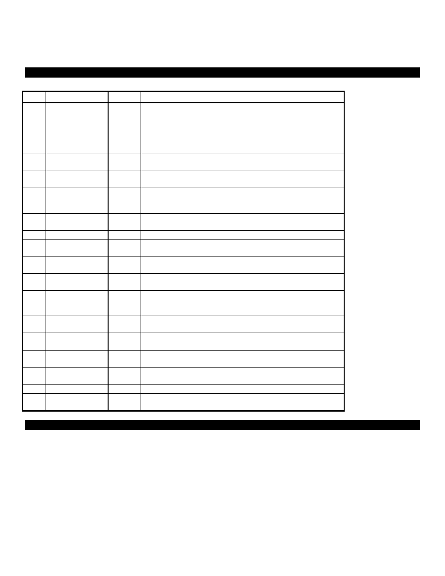
PIN Description
PIN SYMBOL
TYPE
DESCRIPTION
16 XIN
I
X Channel Data In. Sampled on the falling edge of CLKX during
selected time slots.
18 FSX/SYNC1 I/O X Channel Frame Sync. Master X Channel Frame Sync. signal
followed by the first time slot of transmission. It can be either
input or output by initial setup sequence.
Sync 1. Frame sync. for 1
st
CODEC.
20 XOUT
O
X Channel Data Out. Updated on the rising edge of CLKX
during selected time slots.
27 YIN
I
Y Channel Data In. Sampled on the falling edge of CLKY during
selected time slots.
25 FSY
I/O Y Channel Frame Sync. Master X Channel Frame Sync. signal
followed by the first time slot of transmission. It can be either
input or output by initial setup sequence.
24 YOUT
O
Y Channel Data Out. Updated on the rising edge of CLKY
during selected time slots.
2 RSTZ
I
Reset. Low active signal to force chip reset.
13
12
XTAL1/MCLK
XTAL2
I
O
Crystal In & Out. 14.318 MHz Crystal connected*.
17 CLKP
I/O PCM Clock. It can be either input created by external control
circuit, or output generated by internal control circuit.
26 CLKA
I/O ADPCM Clock. It can be either input created by external control
circuit, or output generated by internal control circuit.
15
11
10
SYNC2
SYNC3
SYNC4
O
O
O
Sync 2. Frame sync. for 2
nd
CODEC.
Sync 3. Frame sync. for 3
rd
CODEC.
Sync 4. Frame sync. for 4
th
CODEC.
4
3
TM1
TM0
I
I
TM1 &TM0. Tie to Ground for normal operation.
7
6
A1
A0
I
I
A1 & A0. Address ID key for 3-wire serial port. If match, 3-wire
serial port can be enabled for configuration.
22 SDI
I
Serial Data In. Data for configuration on the fly by 3-wire serial
port. Sampled on the rising edge of SCLK with LSB first.
21 SCLK
I
Serial Clock. Used to write to the 3-wire serial port registers.
23 SCSZ
I
Serial Port Chip Select. Low active to enable 3-wire serial port.
28 V
DD
-
Power. 3.3 Volts.
14
19
Vss1
Vss2
-
-
Ground. 0 Volt.
* For clock source other than 14MHz, please contact Atelic Systems.
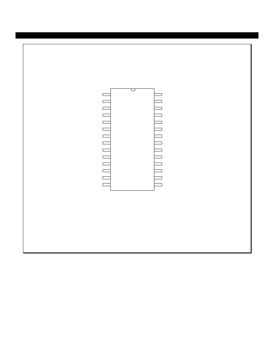
3
Pin Assignment
28-PIN DIP
NC 1
28
RSTZ 2
27
TM0 3
26
TM1 4
25
NC 5
24
A0 6
23
A1 7
22
NC 8
21
NC 9
20
SYNC4 10
19
SYNC3 11
18
XTAL2 12
17
XTAL1 13
16
VSS1 14
15
VDD
YIN
CKLA
FSY
YOUT
SCSZ
SDI
SCLK
XOUT
VSS2
FSX/SYNC1
CLKP
XIN
SYNC2
AT1004 DIP Pin Assignment
1.
When there are multiple AT1004 used on the same system, A1, A0 are used to identify the chip.
2.
A1, A0 are for chip ID. Values are from 00 to 03. They should be connected to microcontroller I/O line or hard wired to either VCC or ground.

4
AT1004 Block Diagram
8-bit PCM from
Combo
8-bit PCM to Combo
Echo
Canceling
Conferencing up to 4
sources
Conferencing up to 4
sources
4
4
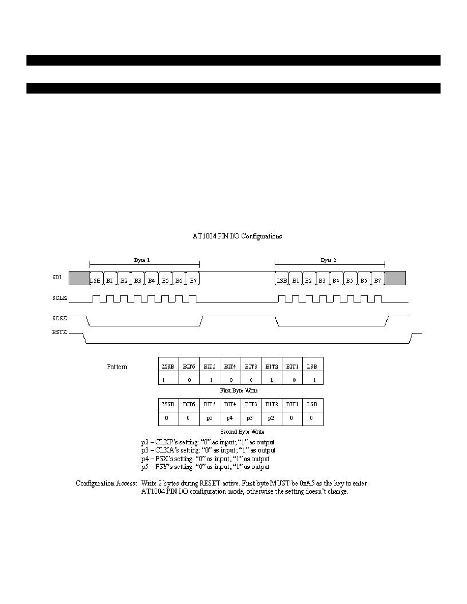
AT1004 Function Diagram
ADPCM Signal
ADPCM Signal
Law to
Linear
ADPCM
Encoder
ADPCM
Decoder
Linear
to Law
Gain
Gain
-
Figure: Block Diagram of conferencing, echo canceling and ADPCM parts. Only one full channel is shown. AT1004
has additional capability to process 4 full channels simultaneously.
5
Power
The AT1004 is powered by a 3.3 V source and draws 60-70 mA at full operation and < 1 mA in powerdown mode.
Initialization
There are two different classes of resets available on the AT1004 chip. For the default reset, hold the RSTZ pin low for 50 ms. This
reset will bring the chip to a functioning default state. In the default state, the following parameters are set:
1.
Pins FSX, FSY, CLKP, CLKA default to input (chip will receive these signals from external source)
2.
4 channels of 32k -law ADPCM decoder running on channels 0-3
3.
4 channels of 32k -law ADPCM encoder running on channels 4-7
4.
4 echo canceling-pairs defined as follows:
a. ADPCM decode channel 0 as reference for ADPCM encode channel 4
b. ADPCM decode channel 1 as reference for ADPCM encode channel 5
c. ADPCM decode channel 2 as reference for ADPCM encode channel 6
d. ADPCM decode channel 3 as reference for ADPCM encode channel 7
5.
No Conferencing is selected
A second type of reset involving the use of the 3-wire serial interface can also be used direct the pin I/O configurations of FSX, FSY,
CLKP, and CLKA during reset.