Äîêóìåíòàöèÿ è îïèñàíèÿ www.docs.chipfind.ru
Specifications and information are subject to change without notice.
WJ Communications, Inc
·
Phone 1-800-WJ1-4401
·
FAX: 408-577-6621
·
e-mail: sales@wj.com
·
Web site: www.wj.com
September
2004
AH1-1
High Dynamic Range Amplifier
Product Information
The Communications Edge
TM
Product Features
·
250 3000 MHz
·
+41 dBm OIP3
·
2.7 dB Noise Figure
·
13.5 dB Gain
·
+21 dBm P1dB
·
Lead-free/Green/
RoHS-compliant
SOT-89 Package
·
Single +5 V Supply
·
MTTF > 100 years
Applications
·
Mobile Infrastructure
·
CATV / DBS
·
W-LAN / ISM
·
RFID
·
Defense / Homeland Security
·
Fixed Wireless
Product Description
The AH1-1 is a high dynamic range amplifier in a low-cost
surface-mount package. The combination of low noise
figure and high output IP3 at the same bias point makes it
ideal for receiver and transmitter applications. The AH1-1
is a specially screened version of the AH1 offering a very
narrow gain spread from device to device.
The device combines dependable performance with superb
quality to maintain MTTF values exceeding 100 years at
mounting temperatures of +85
°C. The AH1-1 is available
in both the standard SOT-89 package and the
environmentally-friendly lead-free/green/RoHS-compliant
SOT-89 package.
The broadband amplifier uses a high reliability GaAs
MMIC technology and is targeted for applications where
high linearity is required. It is well suited for various
current and next generation wireless technologies such as
GPRS, GSM, CDMA, and W-CDMA. In addition, the
AH1-1 will work for other applications within the 250 to
3000 MHz frequency range such as fixed wireless.
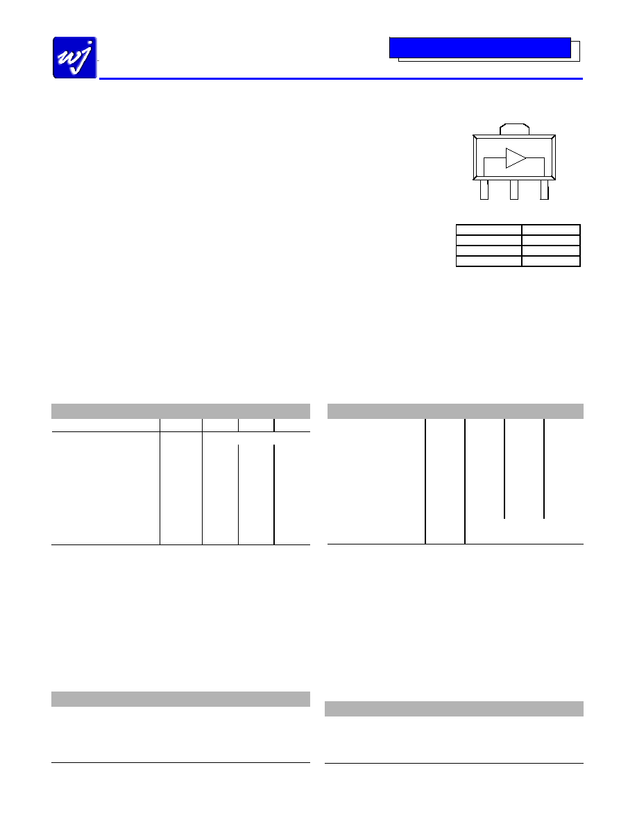
Functional Diagram
RF IN
GND
RF OUT
GND
1
2
3
4
Function Pin
No.
Input 1
Output/Bias 3
Ground 2,
4
Specifications
(1)
Parameter
Units Min Typ Max
Operational Bandwidth
MHz
250
3000
Test Frequency
MHz
800
Gain
dB 12.9 13.3 13.8
Input
Return
Loss
dB 8
Output Return Loss
dB
15
Output P1dB
dBm
+21
Output IP3
(2)
dBm
+37
+41
Noise Figure
(3)
dB 2.7
Operating Current Range
mA
120
150
180
Supply Voltage
V
5
1. Test conditions unless otherwise noted: T = 25º C, 50
system.
2. 3OIP measured with two tones at an output power of +5 dBm/tone separated by 10 MHz. The
suppression on the largest IM3 product is used to calculate the 3OIP using a 2:1 rule.
3. Noise figure can be optimized by matching the input for optimal return loss.
Absolute Maximum Rating
Parameter
Rating
Operating Case Temperature
-40 to +85
°C
Storage Temperature
-55 to +150
°C
Supply Voltage
+6 V
RF Input Power (continuous)
+10 dBm
Junction Temperature
+220
°C
Operation of this device above any of these parameters may cause permanent damage.
Typical Performance
(4)
Parameter
Units
Typical
Frequency MHz
900
1900
2140
S21
dB 14.2 12.2 12.0
S11 dB
-21
-14
-21
S22 dB
-14
-13
-11
Output P1dB
dBm
+21.7
+22
+22
Output IP3
(2)
dBm +42 +41 +40
IS-95 Channel Power
(5)
dB
+15.5 +16.5
Noise Figure
dB
2.2
2.9
2.9
Supply Voltage
V
5
Device Current
mA
150
4. Parameters reflect performance in an AH1-PCB application circuit, as shown on page 3.
5. Measured with -45 dBc ACPR, IS-95 9 channels fwd.
Ordering Information
Part No.
Description
AH1-1
High Dynamic Range Amplifier
(leaded SOT-89 Pkg)
AH1-1G
High Dynamic Range Amplifier
(lead-free/green/RoHS-compliant SOT-89 Pkg)
AH1-PCB
0.8 2.5 GHz Fully Assembled Application Circuit
Specifications and information are subject to change without notice.
WJ Communications, Inc
·
Phone 1-800-WJ1-4401
·
FAX: 408-577-6621
·
e-mail: sales@wj.com
·
Web site: www.wj.com
September
2004
AH1-1
High Dynamic Range Amplifier
Product Information
The Communications Edge
TM
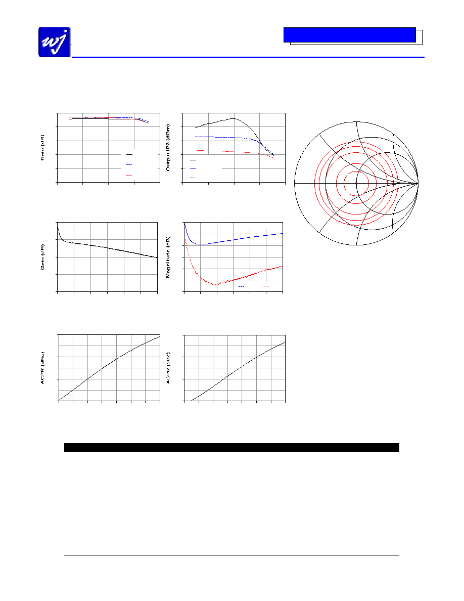
Typical Device Data
S-Parameters (V
DS
= +5 V, I
DS
= 150 mA, T = 25
°C, unmatched device in a 50 ohm system)
Input return loss can be improved with the appropriate input matching network shown later in this datasheet.
Gain vs. Output Power
9
10
11
12
13
14
0
5
10
15
20
Output Power (dBm)
100% Idss
75% Idss
50% Idss
Output IP3 vs. Output Power
20
25
30
35
40
45
0
5
10
15
20
Output Power (dBm)
100% Idss
75% Idss
50% Idss
900 MHz
Gain vs. Frequency
0
5
10
15
20
0
500
1000
1500
2000
2500
3000
Frequency (MHz)
Return Loss vs. Frequency
-30
-25
-20
-15
-10
-5
0
0
500
1000
1500
2000
2500 3000
Frequency (MHz)
S11
S22
w/o Matching Circuitry
ACPR vs. Channel Power
IS-95, 9 Ch. Fwd, ±885 kHz offset, 30 kHz Meas BW, 900 MHz
-70
-60
-50
-40
10
11
12
13
14
15
16
17
Output Channel Power (dBm)
ACPR vs. Channel Power
IS-95, 9 Ch. Fwd, ±885 kHz offset, 30 kHz Meas BW, 1900 MHz
-70
-60
-50
-40
10
11
12
13
14
15
16
17
Output Channel Power (dBm)
S-Parameters (V
D
= +5 V, I
D
= 150 mA, T = 25
°C, calibrated to device leads)
Freq (MHz)
S11 (dB)
S11 (ang)
S21 (dB)
S21 (ang)
S12 (dB)
S12 (ang)
S22 (dB)
S22 (ang)
50 -2.24 -0.36 17.17 164.69 -23.16 50.85 -5.86 -33.21
250 -4.76 -0.36 15.74 161.34 -20.54 31.24 -8.86 -47.02
500 -7.30 -0.30 14.67
160.30
-19.45
14.79
-13.03
-52.43
750 -8.66 -0.30 14.11
154.63
-19.15 3.75 -16.72
-49.89
1000 -8.70 -0.34 13.83 146.75
-19.05 -1.71 -18.22 -48.40
1250 -8.32 -0.38 13.62 138.48
-18.99 -5.88 -19.16 -52.48
1500 -7.78 -0.41 13.36 129.80
-18.99 -9.79 -20.14 -59.84
1750 -7.32 -0.41 13.03 121.57 -18.96 -12.84 -20.93 -68.57
2000 -6.82 -0.40 12.80 113.51 -18.87 -16.17 -21.11 -76.23
2250 -6.46 -0.37 12.52 104.74 -18.89 -19.71 -21.15 -83.31
2500 -6.24 -0.32 12.14 96.55 -18.93 -23.30 -21.55 -90.61
2750 -5.74 -0.26 11.81 88.90 -18.93 -26.26 -22.52 -94.38
3000 -5.25 -0.19 11.45 81.33 -18.92 -29.49 -24.14
-104.23
VSWR=2
VSWR=3
VSWR=4
VSWR=5
IP3=41
IP3=38
IP3=37
IP3=36
IP3=35
IP3=39
VSWR=1.5
OIP3 Load Pull Circles
900 MHz
Specifications and information are subject to change without notice.
WJ Communications, Inc
·
Phone 1-800-WJ1-4401
·
FAX: 408-577-6621
·
e-mail: sales@wj.com
·
Web site: www.wj.com
September
2004
AH1-1
High Dynamic Range Amplifier
Product Information
The Communications Edge
TM
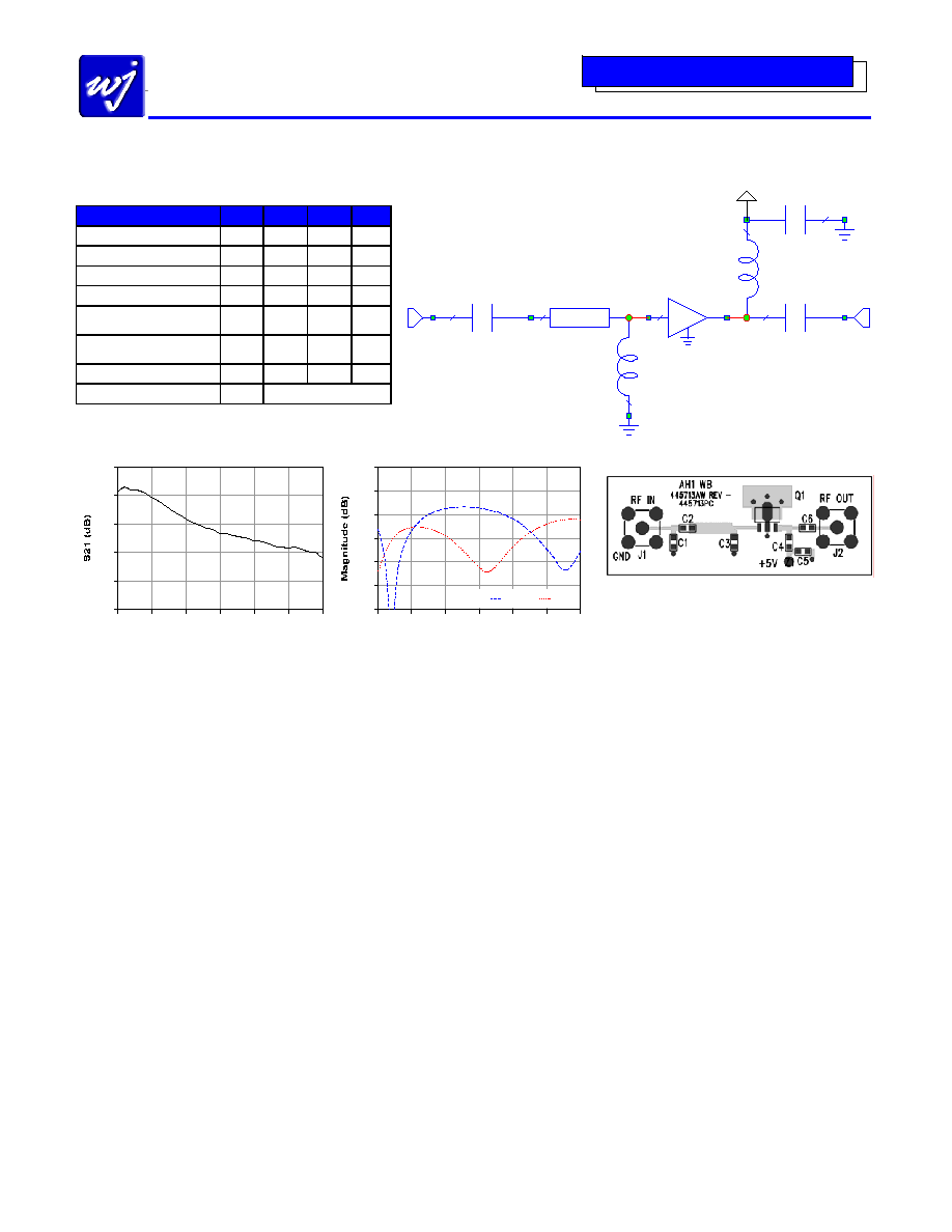
Application Circuit: 800 2500 MHz (AH1-PCB)
Typical RF Performance at 25
°C
Frequency
Units 900
1900 2140
S21 Gain
dB
14.2
12.2 12.0
S11 Input R.L.
dB
-21 -14 -21
S22 Output R.L.
dB
-14 -13 -11
Output P1dB
dB
+21.7 +22 +22
Output IP3
(+5 dBm / tone, 10 MHz spacing)
dB
+42 +41 +40
IS-95 Channel Power
(@-45 dBc ACPR, 9 channels fwd)
dB
+15.5 +16.5
Noise Figure
dB
2.2 2.9 2.9
Device Bias
+5V @ 150mA
C=
ID=
56 pF
C2
C=
ID=
56 pF
C6
C=
ID=
56 pF
C5
L=
ID=
12 nH
C4
L=
ID=
5.6 nH
C3
F0=
EL=
Z0=
0.9 GHz
15.2 Deg
22 Ohm
NET=
ID=
"AH1"
Q1
Vcc = +5 V
All passive components are of size 0603 unless otherwise noted.
configuration.
Component C1 is shown in the silkscreen but is not used for this
Gain
10
11
12
13
14
15
750
1000
1250
1500
1750
2000
2250
Frequency (MHz)
Return Loss
-30
-25
-20
-15
-10
-5
0
750
1000 1250
1500
1750
2000 2250
Frequency (MHz)
S11
S22
Circuit Board Material: .062" total thickness with
a .014" FR-4 top RF layer, 4 layers (other layers
added for rigidity), 1 oz copper, 50
Microstrip line
details: width = .025".
Specifications and information are subject to change without notice.
WJ Communications, Inc
·
Phone 1-800-WJ1-4401
·
FAX: 408-577-6621
·
e-mail: sales@wj.com
·
Web site: www.wj.com
September
2004
AH1-1
High Dynamic Range Amplifier
Product Information
The Communications Edge
TM
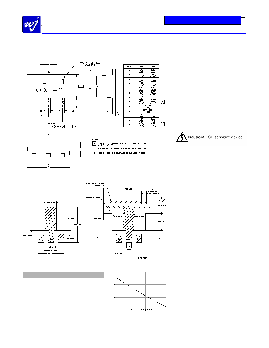
AH1-1 (SOT-89 Package) Mechanical Information
This package may contain lead-bearing materials. The plating material on the leads is SnPb.
Outline Drawing
Land Pattern
Thermal Specifications
Parameter
Rating
Operating Case Temperature
-40 to +85
°C
Thermal Resistance, Rth
(1)
59
° C / W
Junction Temperature, Tjc
(2)
129
° C
1. The thermal resistance is referenced from the hottest
part of the junction to the ground tab (pin 4).
2. This corresponds to the typical biasing condition of
+5V, 150 mA at an 85
°C case temperature. A
minimum MTTF of 1 million hours is achieved for
junction temperatures below 160
°C.
Product Marking
The AH1-1 will be marked with an "AH1"
designator. An alphanumeric lot code
("XXXX-X") is also marked below the part
designator on the top surface of the package.
A "1" will be lasermarked in the upper right-
hand corner.
Tape and reel specifications for this part are
located on the website in the "Application
Notes" section.
MSL / ESD Rating
ESD Rating: Class 1B
Value: Passes
500V to <1000V
Test:
Human Body Model (HBM)
Standard:
JEDEC Standard JESD22-A114
ESD Rating: Class IV
Value: Passes
1000V to <2000V
Test:
Charged Device Model (CDM)
Standard:
JEDEC Standard JESD22-C101
MSL Rating: Level 3 at +235
° C convection reflow
Standard:
JEDEC Standard J-STD-020
Mounting Config. Notes
1. Ground / thermal vias are critical for the proper
performance of this device. Vias should use a .35mm
(#80 / .0135") diameter drill and have a final plated
thru diameter of .25 mm (.010").
2. Add as much copper as possible to inner and outer
layers near the part to ensure optimal thermal
performance.
3. Mounting screws can be added near the part to fasten
the board to a heatsink. Ensure that the ground /
thermal via region contacts the heatsink.
4. Do not put solder mask on the backside of the PC board
in the region where the board contacts the heatsink.
5. RF trace width depends upon the PC board material
and construction.
6. Use 1 oz. Copper minimum.
7. All dimensions are in millimeters (inches). Angles are
in degrees.
MTTF vs. GND Tab Temperature
1
10
100
1000
60
70
80
90
100
110
Tab Temperature (°C)
M
T
TF
(
m
i
l
l
i
on hr
s
)
Specifications and information are subject to change without notice.
WJ Communications, Inc
·
Phone 1-800-WJ1-4401
·
FAX: 408-577-6621
·
e-mail: sales@wj.com
·
Web site: www.wj.com
September
2004
AH1-1
High Dynamic Range Amplifier
Product Information
The Communications Edge
TM
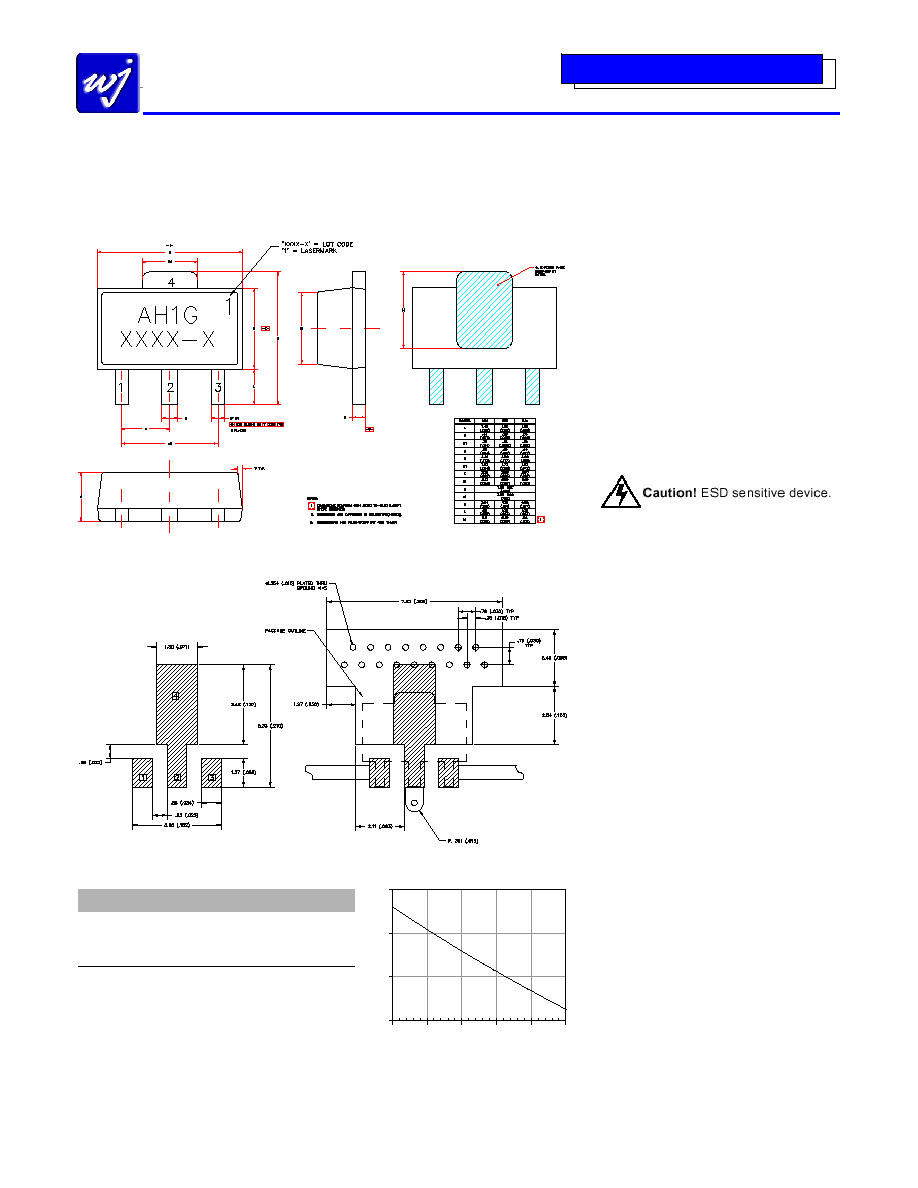
AH1-1G (Green / Lead-free SOT-89 Package) Mechanical Information
This package is lead-free/Green/RoHS-compliant. It is compatible with both lead-free (maximum 260
°C reflow temperature) and leaded
(maximum 245
°C reflow temperature) soldering processes. The plating material on the leads is NiPdAu.
Outline Drawing
Land Pattern
Thermal Specifications
Parameter
Rating
Operating Case Temperature
-40 to +85
°C
Thermal Resistance, Rth
(1)
59
° C / W
Junction Temperature, Tjc
(2)
129
° C
1. The thermal resistance is referenced from the hottest
part of the junction to the ground tab (pin 4).
2. This corresponds to the typical biasing condition of
+5V, 150 mA at an 85
°C case temperature. A
minimum MTTF of 1 million hours is achieved for
junction temperatures below 160
°C.
Product Marking
The AH1-1G will be marked with an
"AH1G" designator. An alphanumeric lot
code ("XXXX-X") is also marked below the
part designator on the top surface of the
package. A "1" will be lasermarked in the
upper right-hand corner.
Tape and reel specifications for this part are
located on the website in the "Application
Notes" section.
MSL / ESD Rating
ESD Rating: Class 1B
Value: Passes
500V to <1000V
Test:
Human Body Model (HBM)
Standard:
JEDEC Standard JESD22-A114
ESD Rating: Class IV
Value: Passes
1000V to <2000V
Test:
Charged Device Model (CDM)
Standard:
JEDEC Standard JESD22-C101
MSL Rating: Level 3 at +260
° C convection reflow
Standard:
JEDEC Standard J-STD-020
Mounting Config. Notes
1. Ground / thermal vias are critical for the proper
performance of this device. Vias should use a .35mm
(#80 / .0135") diameter drill and have a final plated
thru diameter of .25 mm (.010").
2. Add as much copper as possible to inner and outer
layers near the part to ensure optimal thermal
performance.
3. Mounting screws can be added near the part to fasten
the board to a heatsink. Ensure that the ground /
thermal via region contacts the heatsink.
4. Do not put solder mask on the backside of the PC board
in the region where the board contacts the heatsink.
5. RF trace width depends upon the PC board material
and construction.
6. Use 1 oz. Copper minimum.
7. All dimensions are in millimeters (inches). Angles are
in degrees.
MTTF vs. GND Tab Temperature
1
10
100
1000
60
70
80
90
100
110
Tab Temperature (°C)
M
T
TF
(
m
i
l
l
i
on hr
s
)