Specifications and information are subject to change without notice
WJ Communications, Inc
·
Phone 1-800-WJ1-4401
·
FAX: 408-577-6621
·
e-mail: sales@wj.com
·
Web site: www.wj.com
September
2003
The Communications Edge
TM
AH103
High Gain, High Linearity ˝ Watt Amplifier
Product Information
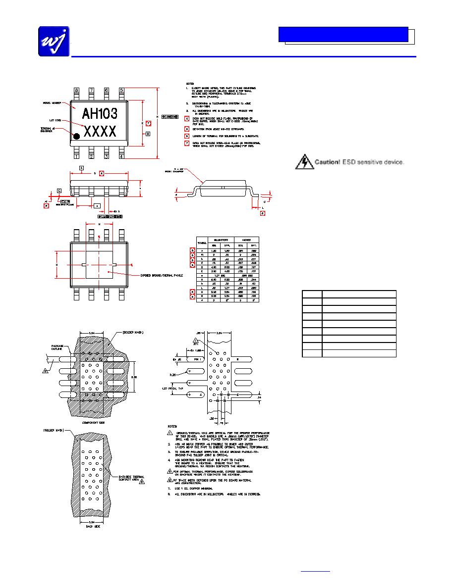
Outline Drawing
Mounting Configuration / Land Pattern
Product Marking
The component will be marked with an "AH103"
designator followed by a four- or five-digit alpha-
numeric lot code on the top surface of the
package. Tape and reel specifications for this
part is located on the website in the "Application
Notes" section.
ESD / MSL Information
ESD Classification: Class 1B
Value: Passes
! 500 V to < 1000 V
Test:
Human Body Model (HBM)
Standard:
JEDEC Standard JESD22-A114
ESD Classification: Class IV
Value: Passes
! 1000 V
Test:
Charged Device Model (CDM)
Standard:
JEDEC Standard JESD22-C101
MSL Rating:
Level 1 at +250
°
C convection reflow
Standard:
JEDEC Standard J-STD-020B
Functional Pin Layout
Pin Function
1 Amp2
input
2
Amp1 output / Bias Amp1
3 Ground
4
RF input (Amp1 input)
5 Ground
6
RF output (Amp2 output)
7 Bias
Amp2
8 Ground
The backside paddle is the Source and should be
grounded for thermal and electrical purposes. All other
pins should be grounded on the PCB.