
8m Class
DC to AC Inverter
Preliminary
8m052489
Specifications and
Applications Information
page 4.
12/14/00
Endicott Research Group, Inc.
2601 Wayne St., Endicott NY 13760
607-754-9187 Fax 607-754-9255
http://www.ergpower.com
Input
8m Package
Package Configuration
.55[14,0]
2.35[59,7]
3.58[90,9]
.79[20,1]
.043[1,09]
.12[3,05]
.120[3,05]
Dia.(2x)
c
Output
.55[14,0]
.50[12,7]
1
1 2 3 4
Con1-1 Vin(+)
Con1-2 GND
Con1-3 Control *
Con1-4 NC
Pin Descriptions
Con2-1 ACout
Con2-2 ACout
Input Connector
4 pins are 0.315" [8,00] Long,
0.025" [0,63] Square and are
on 0.100" [2,54] Centers.
* Valid when the "C" Jumper
is removed
Output Connector
JST
SM02B-BHSS-1-TB
The ERG 8m052489 (8m Class) low profile dc to ac
inverter is specifically designed to power the Samsung
LTN104S2-L01 LCD display module to a moderate
brightness level from a +5 volt dc source.
This low profile inverter features:
�
Less Than 8 mm in Height
�
LCD Module Specific
�
Display Compatible Output Connector
�
Firm Specifications
�
Application Information
�
Designed, Manufactured and Supported in the
USA
�
Custom Input and Output Voltages
�
Flexible System Interface
�
Notebook Display Head Compatible
Endicott Research Group, Inc.
2601 Wayne St., Endicott NY 13760
607-754-9187
Vin
+
-
1
2
3
Vin
+
-
1
2
3
Vin
+
-
1
2
3
3 Dimming Options
(valid when the "C" jumper is removed)
+Vin
5% - 100%
+Vin
approx. 5 ms*
* should be selected to be
compatible with LCD and
display driver
* value should be low
enough to maintain
minimum tube current
at minimum brightness
Vmin* to +Vin
* Vmin should be high
enough to maintain
minimum tube current
100 Kohms*
(1)
(1)
(1)
Note 1 Input by-pass capacitor (25 uf - 100uf) may be required to
reduce reflected ripple.
Voltage Controlled
Pulse-Width
Modulated Controlled
8m052489
0
Resistive Controlled
8m052489
8m052489
Endicott Research Group, Inc.
page 2.
page 3.
Endicott Research Group, Inc.
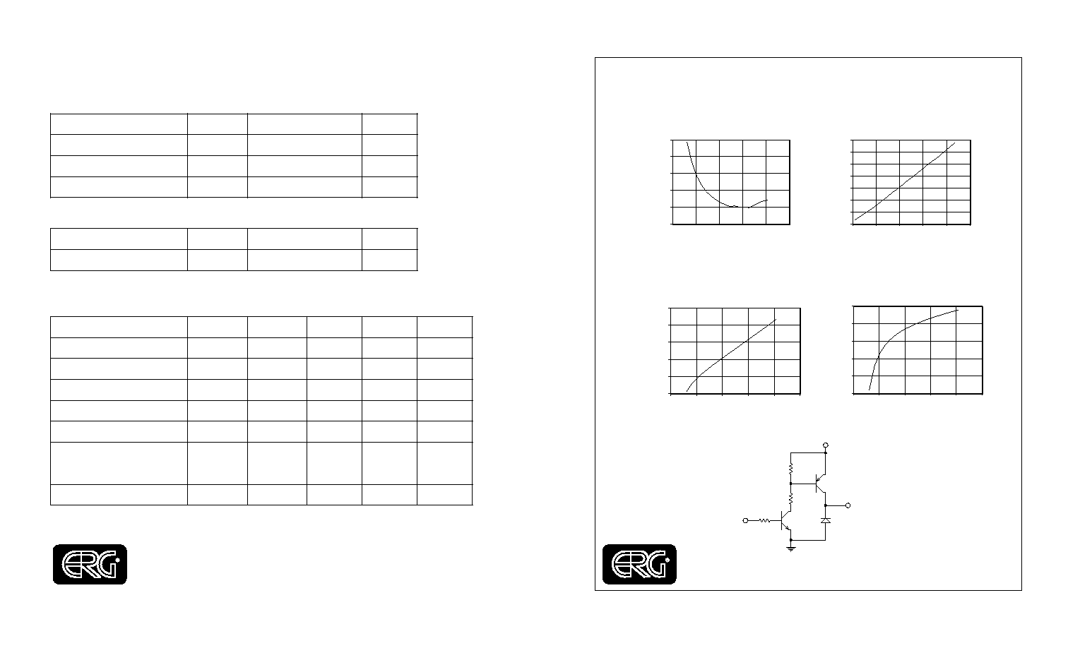
Typical Performance Curves
Made in USA
Input Current vs. Input Voltage
Input Voltage (Vdc)
Input Current (Adc)
0.40
0.50
0.60
0.70
0.80
0.90
2
3
4
5
6
7
Input Power vs. Input Voltage
Input Voltage (Vdc)
Input Power (Watts)
1.00
2.00
3.00
4.00
5.00
6.00
2
3
4
5
6
7
Relative Brightness vs. Input Power
Input Power (Watts)
Relative Brightness
25%
40%
55%
70%
85%
100%
115%
130%
1.00 2.00 3.00 4.00 5.00 6.00
Relative Frequency vs. Input Voltage
Input Voltage (Vdc)
Relative Frequency
-4.0%
0.0%
4.0%
8.0%
12.0%
16.0%
2
3
4
5
6
7
3.3 K
1.5 K
2N3906
2N3904
1 K
+Vin 5V
1N4148
Disable Circuit
Control
Control (pin 3)
Valid with the "C" jumper removed
After tube has been allowed to warm-up for 5 minutes Specifications subject to change without notice.
External Disable Circuit shown on page 3.
s
g
n
it
a
R
m
u
m
i
x
a
M
e
t
u
l
o
s
b
A
g
n
it
a
R
l
o
b
m
y
S
e
u
l
a
V
s
ti
n
U
e
g
n
a
R
e
g
a
tl
o
V
t
u
p
n
I
n
i
V
6
+
o
t
3
.
0
-
c
d
V
e
r
u
t
a
r
e
p
m
e
T
g
n
it
a
r
e
p
O
o
T
0
7
+
o
t
0
-
o
C
e
r
u
t
a
r
e
p
m
e
T
e
g
a
r
o
t
S
g
t
s
T
5
8
+
o
t
0
4
-
o
C
s
n
o
it
i
d
n
o
C
g
n
it
a
r
e
p
O
d
e
d
n
e
m
m
o
c
e
R
g
n
it
a
R
l
o
b
m
y
S
e
u
l
a
V
s
ti
n
U
e
g
a
tl
o
V
t
u
p
n
I
n
i
V
5
.
5
o
t
3
+
c
d
V
s
c
it
s
ir
e
t
c
a
r
a
h
C
l
a
c
ir
t
c
e
l
E
5
2
=
a
T
d
n
a
c
d
s
tl
o
V
0
0
.
5
=
n
i
V
d
e
t
o
n
e
s
i
w
r
e
h
t
o
s
s
e
l
n
U
o
C
c
it
s
ir
e
t
c
a
r
a
h
C
l
o
b
m
y
S
n
i
M
p
y
T
x
a
M
s
ti
n
U
t
n
e
rr
u
C
t
u
p
n
I
n
iI
-
3
8
.
2
9
.
c
d
A
y
c
n
e
u
q
e
r
F
g
n
it
a
r
e
p
O
o
F
6
3
1
4
6
4
z
H
K
e
g
a
tl
o
V
t
u
p
t
u
O
m
u
m
i
n
i
M
)
n
i
m
(
t
u
o
V
0
0
4
1
-
-
s
m
r
V
y
c
n
e
i
c
if
f
E
-
0
8
-
%
t
n
e
rr
u
C
t
u
p
t
u
O
t
u
o
I
-
6
-
s
m
r
a
m
e
g
a
tl
o
V
t
u
p
t
u
O
p
r
a
h
S
a
g
n
ir
e
w
o
p
n
e
h
W
(
).
y
a
l
p
s
i
d
7
6
3
D
0
1
Q
L
t
u
o
V
-
0
0
5
-
s
m
r
V
t
n
e
m
e
ri
u
q
e
R
t
n
e
rr
u
C
t
u
p
n
I
3
n
i
P
-
-
9
1
-
c
d
a
m