e
1
PTF 10154
85 Watts, 1.931.99 GHz
GOLDMOS
®
Field Effect Transistor
Package 20248
0
20
40
60
80
100
0
3
6
9
12
15
Input Power (Watts)
P
o
wer
Ou
tp
u
t
(Watts)
0
10
20
30
40
50
Ef
f
i
ci
ency (
%
)
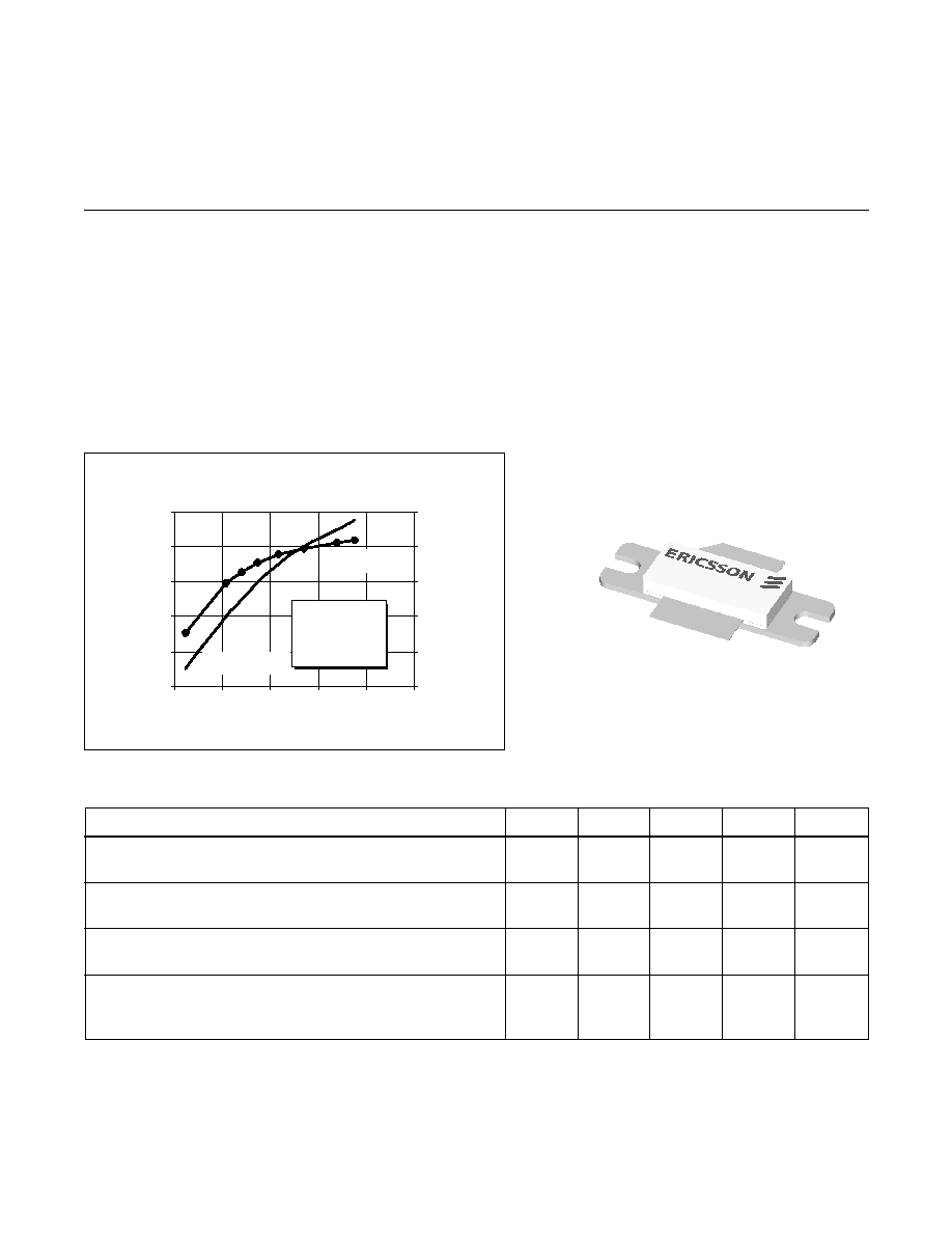
x
V
DD
= 28 V
I
DQ
= 1.15 A
f = 1990 MHz
Typical Power Output and Efficiency
vs. Input Power
Pow er Output
Efficiency
Description
The PTF 10154 is an internally matched 85watt GOLDMOS FET
intended for CDMA and TDMA applications from 1.93 to 1.99 GHz.
This device operates at 43% efficiency with 11 dB gain. Nitride surface
passivation and full gold metallization ensure excellent device life-
time and reliability.
·
INTERNALLY MATCHED
·
Guaranteed Performance at 1.93, 1.99 GHz,
28 V
- Output Power = 85 Watts Min
- Power Gain = 11 dB Typ
·
Full Gold Metallization
·
Silicon Nitride Passivated
·
Back Side Common Source
·
Excellent Thermal Stability
·
100% Lot Traceability
RF Specifications
(100% Tested)
Characteristic
Symbol
Min
Typ
Max
Units
Gain
(V
DD
= 28 V, P
OUT
= 10 W, I
DQ
= 1.15 A, f = 1.96, 1.99 GHz)
G
ps
10.0
11
--
dB
Power Output at 1 dB Compression
(V
DD
= 28 V, I
DQ
= 1.15 A, f = 1.99 GHz)
P-1dB
85
--
--
Watts
Drain Efficiency
(V
DD
= 28 V, P
OUT
= 90 W, I
DQ
= 1.15 A, f = 1.99 GHz)
h
D
--
43
--
%
Load Mismatch Tolerance
(V
DD
= 28 V, P
OUT
= 90 W, I
DQ
= 1.15 A, f = 1.99 GHz
Y
--
--
10:1
--
--all phase angles at frequency of test)
All published data at T
CASE
= 25°C unless otherwise indicated.
10154
A-1234560035

PTF 10154
2
e
Power Gain vs. Output Power
8
9
10
11
12
1
10
100
Output Power (Watts)
Powe
r
Ga
in (dB
)
V
DD
= 28 V
f = 1990 MHz
I
DQ
= 1.2
I
DQ
= 0.6
I
DQ
= 0.3
Electrical Characteristics
(100% Tested)
Characteristic
Conditions
Symbol
Min
Typ
Max
Units
Drain-Source Breakdown Voltage V
GS
= 0 V, I
D
= 100 mA
V
(BR)DSS
65
--
--
Volts
Zero Gate Voltage Drain Current
V
DS
= 28 V, V
GS
= 0 V
I
DSS
--
--
5.0
mA
Gate Threshold Voltage
V
DS
= 10 V, I
D
= 150 mA
V
GS(th)
3.0
--
5.0
Volts
Forward Transconductance
V
DS
= 10 V, I
D
= 2 A
g
fs
--
1.0
--
Siemens
Maximum Ratings
Parameter
Symbol
Value
Unit
Drain-Source Voltage
V
DSS
65
Vdc
Gate-Source Voltage
V
GS
±20
Vdc
Operating Junction Temperature
T
J
200
°C
Total Device Dissipation at
P
D
365
Watts
Above 25°C derate by
2.08
W/°C
Storage Temperature Range
T
STG
40 to +150
°C
Thermal Resistance (T
CASE
= 70°C)
R
q
JC
0.48
°C/W
Typical Performance
Narrowband Test Fixture Performance
0
3
6
9
12
1900
1920
1940
1960
1980
2000
Frequency (MHz)
Gain (dB)
0
10
20
30
40
50
60
V
DD
= 28 V, I
DQ
= 1.15 A
P
OUT
= 85 W
Gain
Return Loss
E
fficiency
R
e
tur
n
Loss
-
5
-
10
-
Ef ficiency

PTF 10154
3
e
Capacitance vs. Supply Voltage *
0
50
100
150
200
250
300
350
0
10
20
30
40
Supply Voltage (Volts)
C
d
s
a
nd C
g
s
(pF)
x
0
5
10
15
20
25
Crss
C
gs
C
ds
C
rss
V
GS
= 0 V
f = 1 MHz
Frequency
Z Source
W
Z Load
W
GHz
R
jX
R
jX
1930
2.9
3.0
1.4
-0.2
1960
2.5
2.6
1.4
-0.9
1990
2.1
1.2
1.4
-1.5
Impedance Data
V
DD
= 28 V, P
OUT
= 85 W, I
DQ
= 1.15 A
Z Source
Z Load
G
S
D
0.95
0.96
0.97
0.98
0.99
1.00
1.01
1.02
1.03
-20
30
80
130
Case Temperature (°C)
Gate-Source Voltage (V)
x
0.600
2.075
3.550
5.025
6.500
7.975
Voltage normalized to 1.0 V
Series show current (A)
Gate-Source Voltage vs. Case Temperature
0.
1
0.1
0.1
-
W
A
V
E
L
E
N
G
T
H
S
T
O
W
A
R
D
G
E
N
E
R
<
--
-
W
A
V
E
L
E
N
G
T
H
S
T
O
W
A
R
D
L
O
A
D
-
0
.
0
Z Load
1990 MHz
1930 MHz
1990 MHz
Z Source
1930 MHz
Z
0
= 50
W
* This part is internally matched. Measurements of the finished
product will not yield these results.
PTF 10154
4
e
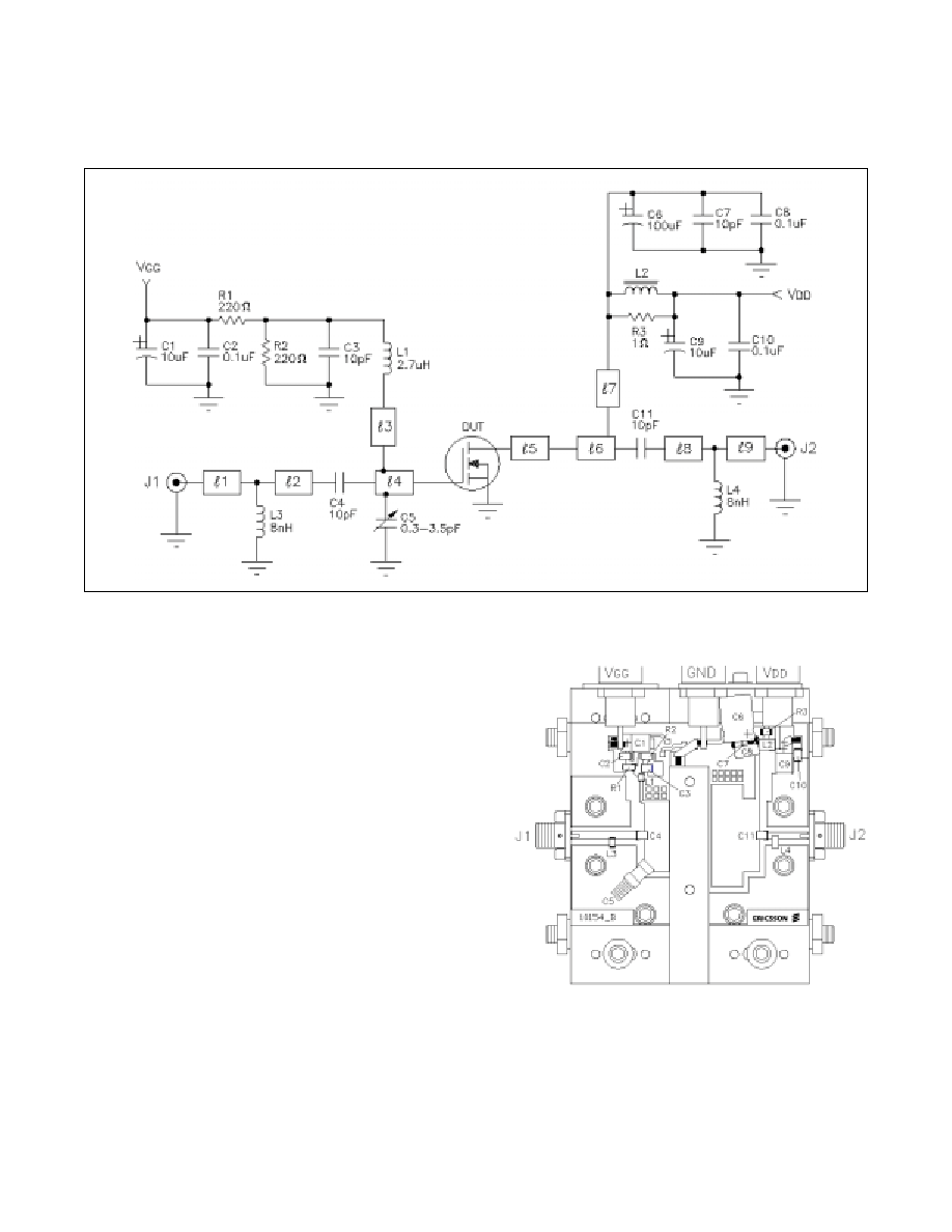
Test Circuit
Test Circuit Block Diagram for f = 1.931.99 GHz
Q1
PTF 10154
LDMOS RF Transistor
Parts Layout (not to scale)
1.96 GHz
IPM (OHMS)
l
1
0.105
l
1.96 GHz Microstrip 50
W
l
2
0.119
l
1.96 GHz Microstrip 50
W
l
3
0.073
l
1.96 GHz Microstrip 76.64
W
l
4
0.094
l
1.96 GHz Microstrip 9.73
W
l
5
0.126
l
1.96 GHz Microstrip 6.67
W
l
6
0.614
l
1.96 GHz Microstrip 9.62
W
l
7
0.170
l
1.96 GHz Microstrip 64.30
W
l
8
0.050
l
1.96 GHz Microstrip 50
W
l
9
0.073
l
1.96 GHz Microstrip 50
W
C1, C9 Capacitor,10µF Digi-Key pcs 6106
C2, C10 Capacitor,0.1µF,50V Digi-Key PCC103BCT
C3, C4, C7, C11 Capacitor,10pF ATC 100 b
C5 Capacitor, variable 0.3-3.5pF JACO johanson 5801
C6 Capacitor,100µF,50V Digi-Key P5182-ND
C8 Capacitor,0.1µF,50V Digi-Key P4525-ND
J1, J2 Connector, SMA female,panel mount
1301-rpm 513 412/53
L1 Chip inductor,2.7µH
L2 Ferrite, 6mm phillips 53/3/4.6-452
L3, L4 Inductor ,8nH coilcraft 0805CS-080 jbc
R1, R2 Resistor, 220 ohm Digi-Key 220 qbk
R3 Resistor, 1 ohm DIGI-KEY 1.0 qbk
Circuit Board 0.050", 2 OZ Copper rogers corporation, TMM6

PTF 10154
5
e
Package Mechanical Specifications
Package 20248
Ericsson Inc.
Microelectronics
Morgan Hill, CA 95037 USA
Specifications subject to change without notice.
LP
© 1999, 2000 Ericsson Inc.
EUS/KR 1522-PTF 10154 Uen Rev. PA3 12-18-00
1-877-GOLDMOS (465-3667) United States
+46 8 757 4700 International
e-mail: rfpower@ericsson.com
www.ericsson.com/rfpower
Primary Dimensions are in inches, altermate dimensions are mm.