37
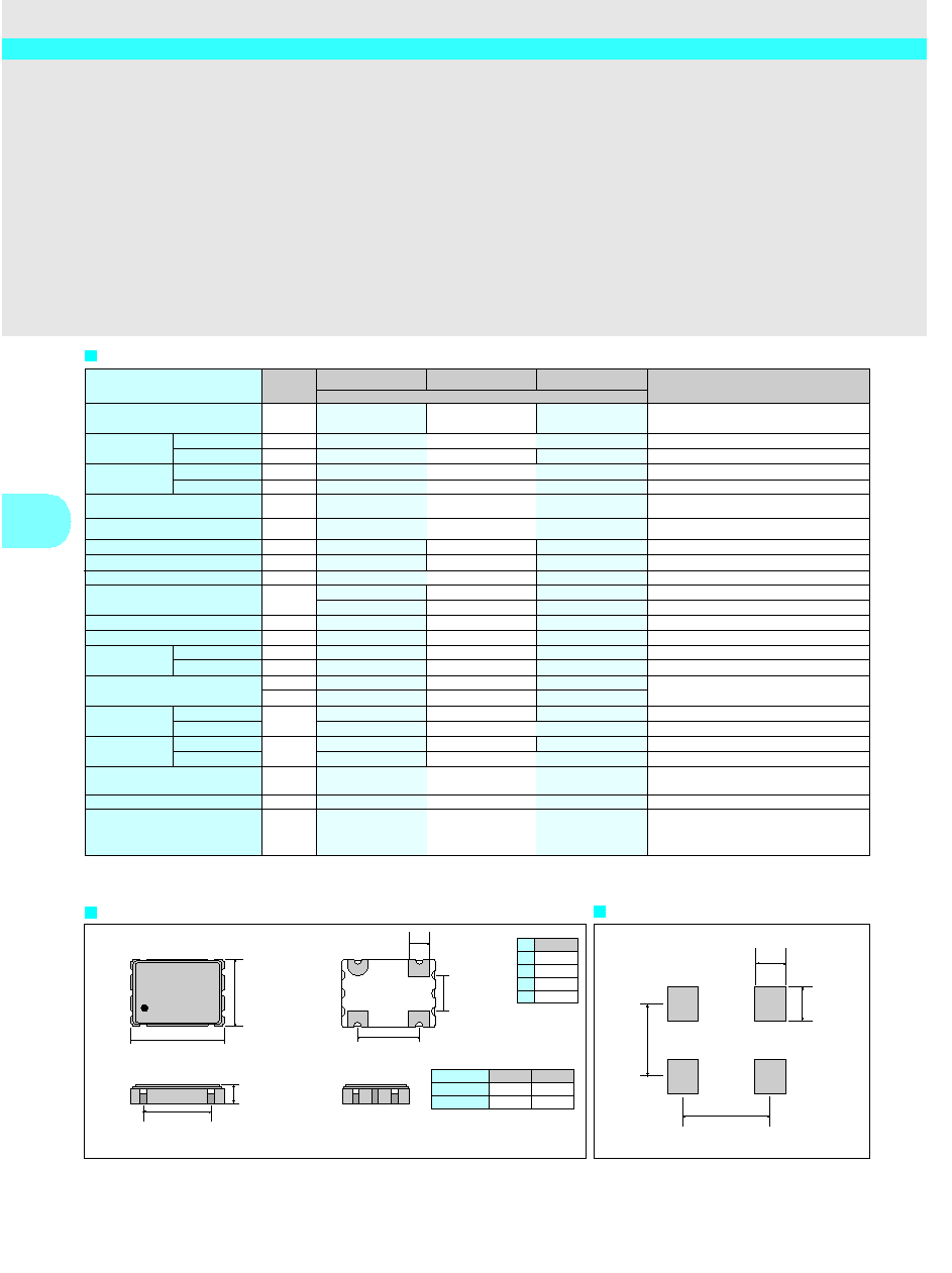
Crystal oscillator
Recommended soldering pattern
(Unit: mm)
1 OE or ST
2 GND
3 OUT
4 V
DD
NO.
7.5 Max.
7.2 Max.
5.0 Max.
5.2 Max.
PTK/PHK/ECK
W
L
5.08
W
E 40.000
HC724A
1.5
Max.
# 3
# 4
# 2
# 1
5.08
1.8
2.0
4.2
5.08
1.4
#1
#2
#4
#3
Bottom View
2.6
External dimensions
Specifications (characteristics)
(Unit: mm)
Pin terminal
L
W
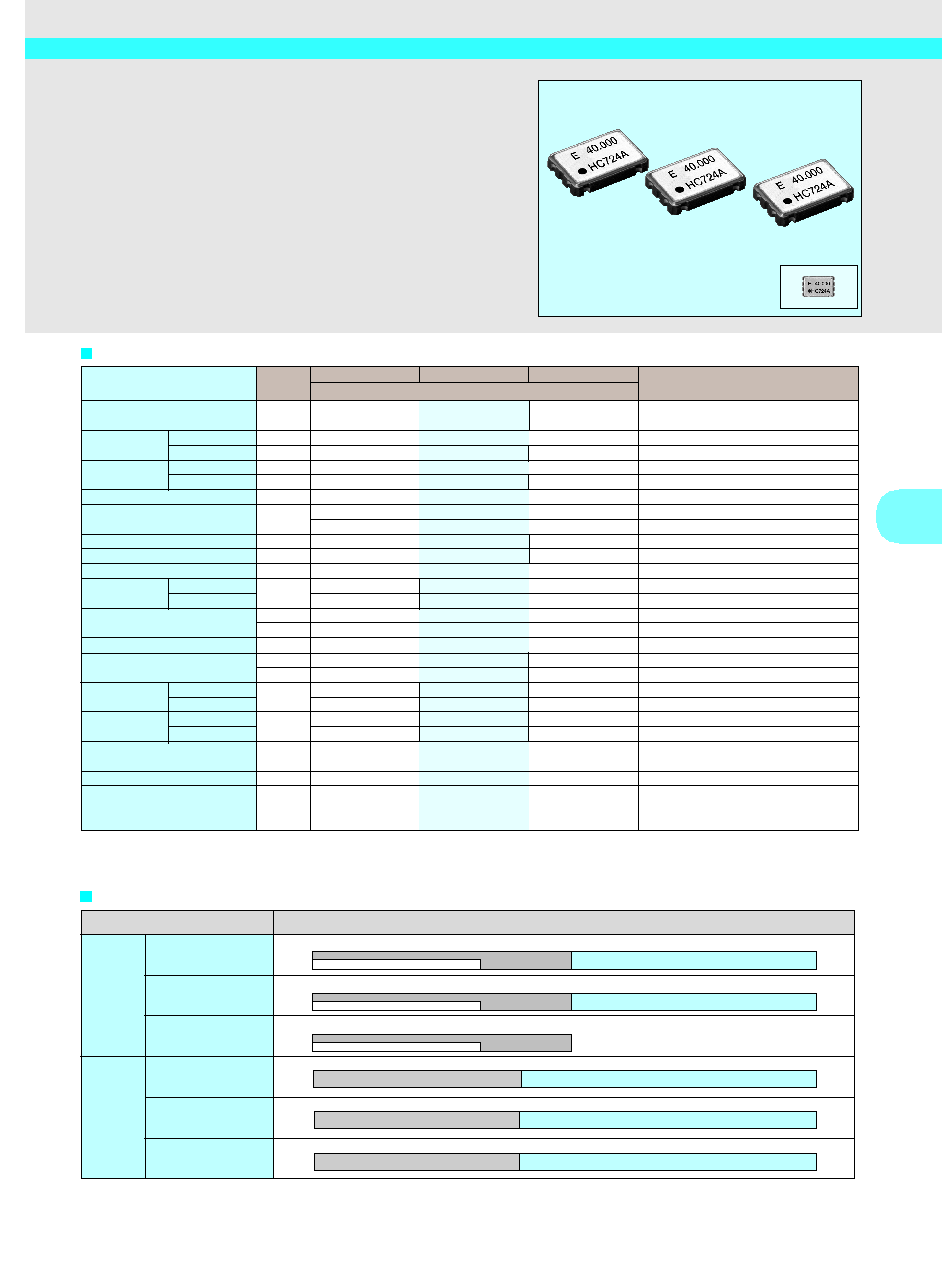
HIGH-FREQUENCY CRYSTAL OSCILLATOR
Item
Output frequency range
Power source
voltage
Temperature
range
Soldering condition
Frequency stability
Current consumption
Output disable current
Standby current
Duty
High output voltage
Low output voltage
Output load
condition (fan out)
Output enable/disable input voltage
Output rise time
Output fall time
Oscillation start up time
Aging
Shock resistance
Symbol
f
0
V
DD
-GND
V
DD
T
STG
T
OPR
T
SOL
f/f
0
Iop
I
OE
I
ST
t
w
/ t
V
OH
V
OL
N
C
L
V
IH
V
IL
t
TLH
t
THL
t
OSC
fa
S.R.
TTL
C-MOS
C-MOS level
TTL level
C-MOS level
TTL level
SG-710PTK
SG-710PHK
SG-710ECK
Specifications
-0.5 V to +7.0 V
5.0
V ±0.5 V
3.3
V ±0.3 V
-55 °C to +125 °C
-10
°C
to +70
°C
(-40
°C
to +85
°C
)
Twice at under +260 °C within 10 s
B: ±50 x 10
-6
C: ± 100 x 10
-6
M: ± 100 x 10
-6
24 mA Max.
40 mA Max.
18 mA Max.
12 mA Max.
16 mA Max.
--
--
10 µA Max.
--
45 % to 55 %
40 % to 60 %
45 % to 55 %
40 % to 60 %
--
2.4 V Min.
V
DD
-0.5 V Min.
0.9
x V
DD
Min.
0.4 V Max.
0.5 V Max.
0.1
x V
DD
Max.
10 TTL Max.
10 TTL Max.
--
(15 pF Max.)
50 pF Max.
15 pF Max.
2.0 V Min.
2.0 V Min.
0.7 x V
DD
Min.
0.8 V Max.
0.8 V Max.
0.3 x V
DD
Max.
--
5 ns Max.
6 ns Max.
5 ns Max.
--
--
5 ns Max.
6 ns Max.
5 ns Max.
--
10 ms Max.
±5 x 10
-6
/year Max.
±10 x 10
-6
Max.
Remarks
B,C:-10 °C to +70 °C, M:-40 °C to +85 C°
No load condition
OE=GND(PTK, PHK)
ST=GND(ECK)
C-MOS load: 1/2 V
DD
level
TTL load: 1.4 V level
I
OH
=-16 mA(PTK,PHK),-2 mA(ECK)
I
OL
= 16 mA(PTK,PHK), 2 mA(ECK)
OE
terminal
(PTK,PHK)
ST
_
terminal
(ECK)
C-MOS load: 10
%
90
%
V
DD
TTL load: 0.4 V
2.4 V
C-MOS load: 90
%
10
%
V
DD
TTL load: 2.4 V
0.4 V
Time at minimum operating voltage to be 0 s
Ta= +25 °C, V
DD
= 5.0 V/3.3 V(ECK)
Three drops on a hard board from 750 mm
or excitation test with 29400 m/s
2
x 0.3 ms x
1/2sine wave in 3 directions
Max. supply voltage
Operating voltage
Storage temperature
Operating temperature
· Ceramic package with 1.5 mm thickness.
· Excellent shock resistance and environmental capability.
· Low current consumption due to use of C-MOS technology.
· Low current consumption by output enabled function (OE) or
standby function (ST).
1.8000 MHz to
50.0000 MHz
1.8000 MHz to
80.0000 MHz
1.8000 MHz to
67.0000 MHz
SG-710 series
Please contact us on availability of -40
°C to +85 °C
38
Actual size
Specifications (characteristics)
Operating condition and Frequency band
100 MHz
50 MHz
1 MHz
150 MHz
Frequency stability:B
( -20 to +70
°C)
SG-710ECK
SG-710PTK
SG-710PHK
SG-710ECK
SG-710ECK
Frequency stability:C
(-20 to +70
°C)
Frequency stability:M
( -40 to +85
°C)
SG-710PCW/SCW
Frequency stability:B
( -20 to +70
°C)
80
1.8
1.8
1.8
1.8
50
Frequency stability:C
( -20 to +70
°C)
SG-710PCW/SCW
Frequency stability:M
( -40 to +85
°C)
Operating condition
SG-710PTW/STW/PHW/SHW
SG-710PTK
SG-710PHK
80
1.8
50
135
SG-710PTW/STW/PHW/SHW
SG-710PTK
SG-710PHK
80
1.8
50
135
26
135
26
135
26
67
67
67
135
3.3 V
±0.3 V
5 V
±0.5 V
SG-710PCW/SCW
SG-710ECK
Output frequency range
Power source
voltage
Temperature
range
Soldering condition (lead part)
Frequency stability
Current consumption
Output disable current
Output disable current
Duty
Output voltage
Output load condition (fan out)
Output enable
disable input voltage
Output
rise time
Output
fall time
Oscillation start up time
Aging
Shock resistance
f
0
V
DD
-GND
V
DD
T
STG
T
OPR
T
SOL
f/f
0
Iop
Io
E
I
ST
tw/t
V
OH
V
OL
C
L
V
IH
V
IL
t
TLH
t
THL
t
OSC
fa
S.R.
C-MOS level
TTL level
C-MOS level
TTL level
C-MOS level
TTL level
SG-710PTW/STW
SG-710PHW/SHW
SG-710PCW/SCW
Specifications
Remarks
80.0001 MHz to 135.0000 MHz
-0.5 V to +7.0 V
5.0
V±0.5 V
3.3
V±0.3 V
-55 °C to +125 °C
-20
°C to +70 °C -40 °C to +85 °C
Twice at under 260
°
C
within 10 s or under 230
°
C
within 3 min.
B: ±50
x 10
-6
C: ±100
x 10
-6
M: ±100
x 10
-6
45 mA Max.
28 mA Max.
30 mA Max.
16 mA Max.
50
µA Max.
-- 40 % to 60 %
40 % to 60 % --
V
DD
-0.4 V Min.
0.4 V Max.
15 pF Max.
10 ms Max.
±5 x 10
-6
/year Max.
±20 x 10
-6
Max.
-20 °C to +70 °C
-40 °C to +85 °C
No load condition
OE=GND(P*W)
ST=GND(S*W)
C-MOS load: 1/2V
DD
TTL load: 1.4 V
I
OH
= -16
m
A (*TW/HW)/-8 mA(
*CW)
I
OL
= -16
m
A (*TW/HW)/8 mA(
*CW)
OE,ST
OE,ST
C-MOS load: 20 %
80 % V
DD
TTL load: 0.4 V
2.4 V
C-MOS load: 80 %
20 % V
DD
TTL load: 2.4 V
0.4 V
Time at 4.5 V to be 0 s
Ta=+25 °C, V
DD
=5 V
Three drops on a hard board from 750 mm or
excitation test with 29400 m/s
2
x 0.3 ms x 1/2
sine wave in 3 directions
Max. supply voltage
Operating voltage
Storage temperature
Operating temperature
66.6667 MHz to
135.0000 MHz
Item
Symbol
0.7 V
DD
Min.
0.2 V
DD
Max.
3 ns Max.
--
3 ns Max.
--
2.0 V Min.
0.8 V Max.
3 ns Max.
--
3 ns Max.
--
--
4 ns Max.
--
4 ns Max.