43
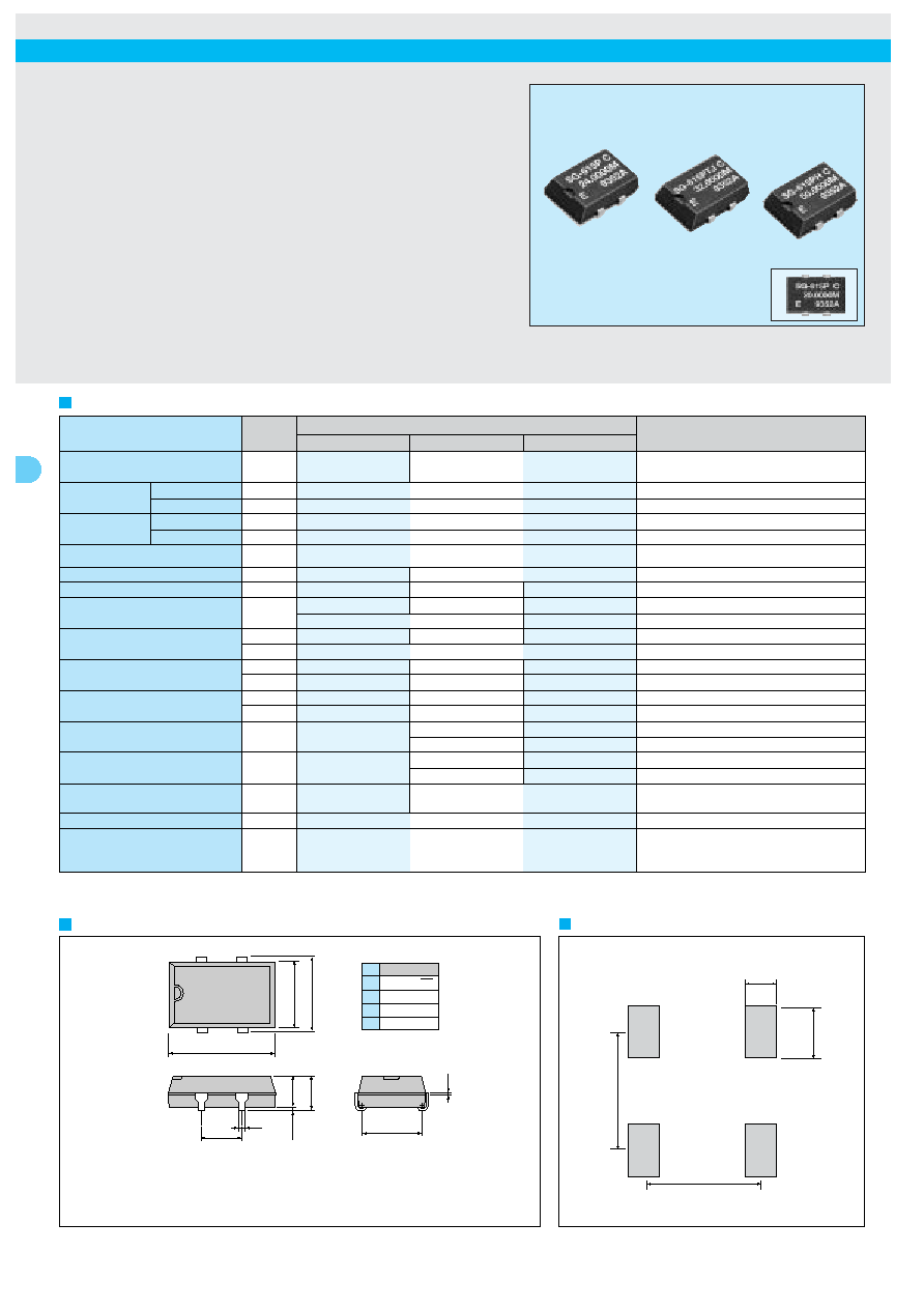
Crystal oscillator
Recommended soldering pattern
(Unit: mm)
1.3
3.0
8.8
5.08
1 OE or ST
2 GND
3 OUT
4 V
DD
NO.
#1
#2
#4
#3
8.65
0.25
9.8 Max.
4.7 Max.
4.06
0.25 Min.
External dimensions
Specifications (characteristics)
(Unit: mm)
14.0 Max.
5.08
7.62
0.51
20.0000M
SG-615PC
9352A
E
Pin terminal
Note.
OE Pin (P, PTJ, PH, PTW, PHW, PCW, PCN)
OE pin - "H" or "open" : Specified frequency output.
OE pin - "L" : Output is high impedance.
ST pin (STW, SHW, SCW)
ST pin - "H" or "open" : Specified frequency output.
ST pin - "L" : Output is low level (weak pull - down), oscillation stops.
SOJ HIGH-FREQUENCY CRYSTAL OSCILLATOR
SG-615 series
Item
Output frequency range
Power source
voltage
Temperature
range
Frequency stability
Current consumption
Output disable current
Duty
Output voltage
Output load
condition (fan out)
Output enable/disable input voltage
Output rise time
Output fall time
Oscillation start up time
Aging
Shock resistance
Symbol
f
0
V
DD
-GND
V
DD
T
STG
T
OPR
f/f
0
Iop
I
OE
t
w
/t
V
OH
V
OL
C
L
N
V
IH
V
IL
t
TLH
t
THL
t
OSC
fa
S.R.
Specifications
SG-615P
SG-615PTJ
SG-615PH
1.0250 MHz to 26.0000 MHz
26.0001 MHz to 66.6667 MHz
-0.3 V to +7.0 V
5.0
V±0.5 V
-55 °
C to +125 °C
-20
°
C
to
+
70
°
C
(-40
°
C
to
+
85
°
C
)
B: ±50 x
10
-6
C: ±100 x
10
-6
23 mA Max.
35 mA Max.
12 mA Max.
28 mA Max.
20 mA Max.
40 % to 60 %
--
40 % to 60 %
45 % to 55 %
--
V
DD
-0.4 V Min.
2.4 V Min.
V
DD
-0.4 V Min.
0.4 V Max.
50 pF Max.
--
50 pF Max.
10 TTL Max.
5 TTL Max.
--
2.0 V Min.
3.5 V Min.
2.0 V Min.
0.8 V Max.
1.5 V Max.
0.8 V Max.
4 ms Max.
10 ms Max.
±5 x 10
-6
/year Max.
±20 x 10
-6
Max.
8 ns Max.
8 ns Max.
--
5 ns Max.
--
5 ns Max.
7 ns Max.
--
7 ns Max.
--
Remarks
Refer to page 31. "Frequency range"
Stored as bare product after unpacking
Refer to page 31. "Frequency range"
B type is possible up to 55 MHz
No load condition
OE=GND
CMOS load: 1/2V
DD
TTL load: 1.4 V
I
OH
= -400 µA (P,PTJ) /-4 mA (PH)
I
OL
= 16 mA (P) /8mA (PTJ) /4 mA (PH)
C
L
<
_
15 pF
I
IH
=1 µA Max.(OE=V
DD
)
I
IL
=-100 µA Min.(OE=GND) , PTJ : I
IL
=-500 µA Min.(OE=GND)
CMOS load: 20
%
80
%
V
DD
TTL load: 0.4 V
2.4 V
CMOS load: 80
%
20
%
V
DD
TTL load: 2.4 V
0.4 V
Time at 4.5 V to be 0 s
Ta= +25 °C, V
DD
= 5 V, first year
Three drops on a hard board from 750 mm
or excitation test with 29400 m/s
2
x 0.3 ms x
1/2sine wave in 3 directions
Note:
· Unless otherwise stated, characteristics (specifications) shown in the above table are based on the rated operating temperature and voltage condition.
· External by-pass capacitor is recommended.
Max. supply voltage
Operating voltage
Storage temperature
Operating temperature
· High-density mounting-type SMD.
· A general-purpose SMD with heat-resisting cylindrical AT-cut crystal unit
and allowing almost the same soldering temperature as SMD IC.
· Cylindrical AT crystal unit builtin, thus assuring high reliability.
· Low current consumption by output enable function(OE) or standby
function(ST).
Actual size
Product number (Please refer to P1)
Q33 6 1 5 x x x x x x x 0 0
44
Crystal oscillator
Specifications (characteristics)
Output frequency range
Power source
voltage
Temperature
range
Frequency stability
Current consumption
Output disable current
Standby current
Duty
Output voltage
Output load condition (fan out)
Output enable
disable input voltage
Output rise time
Output fall time
Oscillation start up time
Aging
Shock resistance
f
O
V
DD-
GND
V
DD
T
STG
T
OPR
f/f
0
I
OP
I
OE
I
ST
tw/t
V
OH
V
OL
CL
V
IH
V
IL
t
TLH
t
THL
t
OSC
fa
S.R.
Refer to page 31. "Frequency range"
Stored as bare product after unpacking
Refer to page 31. "Frequency range"
-20
°
C to +70
°
C
-40
°
C to +85
°
C
No load condition
OE=GND (PCG/PCN)
ST=GND (SCG)
50 % V
DD
, CL = Max.
I
OH
= -8 mA
I
OL
= 8 mA
OE, ST
OE, ST
20 % to 80 % V
DD
, CL
Max.
80 % to 20 % V
DD
CL
Max.
Time at minimum operating voltage to be 0 s
Ta=+25
°
C, V
DD
=3.3 V First year
Item
Remarks
Symbol
Specifications
SG-615PCG
SG-615SCG
SG-615PCN
1.5000 MHz to 26.0000 MHz
26.0001 MHz to 66.6667 MHz
-0.5 V to +7.0 V
2.7 V to 3.6 V
3.0 V to 3.6 V
-55
°
C to +125
°
C
-40
°
C to +85
°
C
B :
±
50 x 10
-6
C :
±
100 x 10
-6
M :
±
100 x 10-6
12 mA Max.
30 mA Max.
10 mA Max.
--
15 mA Max.
--
50
µ
A Max.
--
45 % to 55 %
VDD -0.4 V Min.
2.2 V Min.
0.4 V Max.
0.4 V Max.
25 pF
15 pF
70 % V
DD
Min.
70 % V
DD
Min.
20 % V
DD
Max.
30 % V
DD
Max.
4.0 ns Max.
7 ns
4.0 ns Max.
7 ns
12 ms Max.
10 mS Max.
±
5 x 10
-6
/ year Max.
±
20 x 10
-6
Max.
Max. supply voltage
Operating voltage
Storage temperature
Operating temperature
Specifications (characteristics)
Output frequency range
Power source
voltage
Temperature
range
Frequency stability
Current consumption
Output disable current
Standby current
Duty
Output voltage
Output load condition (fan out)
Output enable disable input voltage
Output rise time
Output fall time
Oscillation start up time
Aging
Shock resistance
f
O
V
DD-
GND
V
DD
T
STG
T
OPR
f/f
0
I
OP
I
OE
I
ST
tw/t
V
OH
V
OL
CL
V
IH
V
IL
t
TLH
t
THL
t
OSC
fa
S.R.
Refer to page 31. "Frequency range"
Stored as bare product after unpacking
Refer to page 31. "Frequency range"
-20
°
C to +70
°
C
-40
°
C to +80
°
C
No load condition
OE=GND(P
W)
ST=GND(S
W)
TTL load : 1.4 V, CL = Max.
TTL load : 1.4 V, 5TTL + 15 pF, fo
66.6667 MHz
CMOS load : 50% V
DD
, CL = Max.
CMOS load : 50% V
DD
, CL = 25 pF, fo
66.6667 MHz
CMOS load : 50% V
DD
, CL = 25 pF, fo
40.0 MHz
I
OH
= -16 mA (
TW/
HW)/-8 mA(
CW)
I
OL
= 16 mA (
TW/
HW)/8 mA(
CW)
fo
135 MHz
fo
90 MHz
fo
66.6667 MHz
fo
135 MHz
fo
125 MHz
fo
66.6667MHz
fo
40.0 MHz
OE,ST
OE,ST
TTL load: 0.8 V
2.0 V, CL = Max.
TTL load: 0.4 V
2.4 V, CL = Max.
CMOS load: 20 %
80 % V
DD
, CL= 25 pF
CMOS load: 20 %
80 % V
DD
, CL= 15 pF
CMOS load: 20 %
80 % V
DD
, CL= Max.
TTL load: 2.0 V
0.8 V, CL = Max.
TTL load: 2.4 V
0.4 V, CL = Max.
CMOS load: 80 %
20 % V
DD
, CL= 25 pF
CMOS load: 80 %
20 % V
DD
, CL= 15 pF
CMOS load: 80 %
20 % V
DD
, CL= Max.
Time at minimum operating voltage to be 0 s
Ta=+25
°
C, VDD =5.0 V / 3.3 V, First year
Item
Remarks
Symbol
Specifications
SG-615PTW/STW
SG-615PHW/SHW
SG-615PCW/SCW
55.0001 MHz to 135.0000 MHz
26.0001 MHz to 135.0000 MHz
-0.5 V to +7.0 V
5.0 V
±
0.5 V
3.3 V
±
0.3 V
-55
°
C to +100
°
C
-20
°
C to +70
°
C
-40
°
C to +85
°
C
B :
±
50 x 10
-6
C :
±
100 x 10
-6
--
M :
±
100 x 10
-6
45 mA Max.
28 mA Max.
30 mA Max.
16 mA Max.
50
µ
A Max.
40 % to 60 %
--
--
45 % to 55 %
--
--
--
40 % to 60 %
40 % to 60 %
--
45 % to 55%
--
--
--
45 % to 55%
V
DD
-0.4 V Min.
0.4 V Max.
15 pF
--
--
5 TTL + 15 pF
--
--
25 pF
--
--
--
15 pF
15 pF
--
25 pF
--
--
50 pF
--
--
--
30 pF
2.0 V Min.
0.7 V
DD
Min.
0.8 V Max.
0.2 V
DD
Max.
2.0 ns Max.
--
--
4.0 ns Max.
--
--
--
3.0 ns Max.
--
--
--
3.0 ns Max.
--
4.0ns Max.
4.0ns Max.
2.0 ns Max.
--
--
4.0 ns Max.
--
--
--
3.0 ns Max.
--
--
--
3.0 ns Max.
--
4.0ns Max.
4.0ns Max.
10 ms Max.
±
5 x 10
-6
/year Max.
±
20 x 10
-6
Max.
Max. supply voltage
Operating voltage
Storage temperature
Operating temperature
Three drops on a hard board from 750 mm or
excitation test with 29400 m/s2 x 0.3 ms x 1/2
sine wave in 3 directions
Three drops on a hard board from 750 mm or
excitation test with 29400 m/s2 x 0.3 ms x 1/2
sine wave in 3 directions