
ˋ 1995 Elantec, Inc.
EL
4450C
General Description
The EL4450C is a complete four-quadrant multiplier circuit. It offers
wide bandwidth and good linearity while including a powerful output
voltage amplifier, drawing modest supply current.
The EL4450C operates on Ý5V supplies and has an analog input range
of Ý2V, making it ideal for video signal processing. AC characteristics
do not vary over the Ý5V to Ý15V supply range.
The multiplier has an operational temperature range of -40¯C to
+85¯C and are packaged in plastic 14-pin P-DIP and SO.
Connection Diagrams
Features
ñ Complete four-quadrant multiplier
with output amp--requires no
extra components
ñ Good linearity of 0.3%
ñ 90 MHz bandwidth for both X and
Y inputs
ñ Operates on Ý5V to Ý15V supplies
ñ All inputs are differential
ñ 400V/çs slew rate
Applications
ñ Modulation/Demodulation
ñ RMS computation
ñ Real-time power computation
ñ Nonlinearity correction/generation
Ordering Information
Part No.
Temp. Range
Package
Outline #
EL4450CN
-40¯C to +85¯C
14-Pin P-DIP
MDP0031
EL4450CS
-40¯C to +85¯C
14-Lead SO
MDP0027
EL4450C
Wideband Four-Quadrant Multiplier
Jan
uary 1996 Rev B
D44450B.fm Page 1 Tuesday, April 21, 1998 9:51 AM

2
EL4450C
Wideband Four-Quadrant Multiplier
E
L
4450C
Absolute Maximum Ratings
(T
A
= 25 ¯C)
V+
Positive Supply Voltage
16.5V
V
S
V+ to V- Supply Voltage
33V
V
IN
Voltage at any Input or Feedback
V+ to V-
V
IN
Difference between Pairs of Inputs or Feedback
6V
I
IN
Current into any Input or Feedback Pin
4 mA
I
OUT
Output Current
30 mA
P
D
Maximum Power Dissipation
See Curves
T
A
Operating Temperature Range
-40¯C to +85¯C
T
S
Storage Temperature Range
-60¯C to +150¯C
Important Note:
All parameters having Min/Max specifications are guaranteed. The Test Level column indicates the specific device testing actually performed during
production and Quality inspection. Elantec performs most electrical tests using modern high-speed automatic test equipment, specifically the LTX77
Series system. Unless otherwise noted, all tests are pulsed tests, therefor T
J
= T
C
= T
A
.
Test Level
Test Procedure
I
100% production tested and QA sample tested per QA test plan QCX0002.
II
100% production tested at T
A
= 25¯C and QA sample tested at T
A
= 25¯C, T
MAX
and T
MIN
per QA test plan QCX0002.
III
QA sample tested per QA test plan QCX0002.
IV
Parameter is guaranteed (but not tested) by Design and Characterization Data.
V
Parameter is typical value at T
A
= 25¯C for information purposes only.
Open-Loop DC Electrical Characteristics
Power Supplies at Ý5V, T
A
= 25¯C, V
FB
= V
OUT
.
Parameter
Description
Min
Typ
Max
Test Level
Units
V
DIFF
Differential Input Voltage--Clipping
1.8
2.0
I
V
0.2% nonlinearity
1.0
V
V
V
CM
Common-Mode Range of V
DIFF
= 0, V
S
= Ý5V
Ý2.5
Ý2.8
I
V
V
S
= Ý15V
Ý12.5
Ý12.8
I
V
V
OS
Input Offset Voltage
8
35
I
mV
I
B
Input Bias Current
9
20
I
çA
I
OS
Input Offset Current between X
IN
+ and X
IN
-, Y
IN
+ and Y
IN
-, REF and FB
0.5
4
I
çA
Gain
Gain Factor of V
OUT
= Gain
æ
X
IN
+
æ
Y
IN
0.45
0.5
0.55
I
V/V
2
NLx
Nonlinearity of X Input; X
IN
between -1V and +1V
0.3
0.7
I
%
NLy
Nonlinearity of Y Input; Y
IN
between -1V and +1V
0.2
0.35
I
%
R
IN
Input resistance
X
IN+
to X
IN-
, Y
IN+
to Y
IN-
,
230
V
k
REF to FB
90
CMRR
Common-Mode Rejection Ratio, X
IN
and Y
IN
70
90
I
dB
PSRR
Power-Supply Rejection Ratio, FB
60
72
I
dB
V
O
Output Voltage Swing
(V
IN
= 0, V
REF
Varied)
V
S
= Ý5V
Ý2.5
Ý2.8
I
V
V
S
= Ý15V
Ý12.5
Ý12.8
I
SC
Output Short-Circuit Current
40
85
I
mA
I
S
Supply Current, V
S
= Ý15V
15.4
18
I
mA
D44450B.fm Page 2 Tuesday, April 21, 1998 9:51 AM

3
EL4450C
Wideband Four-Quadrant Multiplier
EL
4450C
Test Circuit
Typical Performance Curves
Closed-Loop AC Electrical Characteristics
Power Supplies at Ý12V, T
A
= 25¯C, R
L
= 500ƒ, C
L
= 15pF
Parameter
Description
Min
Typ
Max
Test Level
Units
BW, -3 dB
-3 dB Small-Signal Bandwidth, X or Y
90
V
MHz
BW, Ý0.1 dB
0.1 dB Flatness Bandwidth
10
V
MHz
Peaking
Frequency Response Peaking
1.0
V
dB
SR
Slew Rate, V
OUT
between -2V and +2V
300
400
I
V/çs
V
N
Input-Referred Noise Voltage Density
100
V
nV/Hz
Note: For typical performance curves, R
F
= 0, R
G
= æ, V
S
= Ý5V, R
L
= 500ƒ, and C
L
= 15 pF unless otherwise noted.
Transfer Function of X Input for
Various Y Inputs
Transfer Function of Y Input for
Various X Inputs
D44450B.fm Page 3 Tuesday, April 21, 1998 9:51 AM

4
EL4450C
Wideband Four-Quadrant Multiplier
E
L
4450C
Frequency Response
for Various Feedback
Divider Ratios
Frequency Response
for Various R
L
, C
L
V
S
= Ý5V
Frequency Response
for Various R
L
, C
L
V
S
= Ý15V
X Input Frequency Response
for Various Y DC Inputs
Y Input Frequency Response
for Various X DC Inputs
-3 dB Bandwidth
and Peaking
vs Supply Voltage
Change in Bandwidth
and Peaking vs Temperature
Total Harmonic Distortion
of X Input vs Frequency
Total Harmonic Distortion
of Y Input vs Frequency
D44450B.fm Page 4 Tuesday, April 21, 1998 9:51 AM
5
EL4450C
Wideband Four-Quadrant Multiplier
EL
4450C
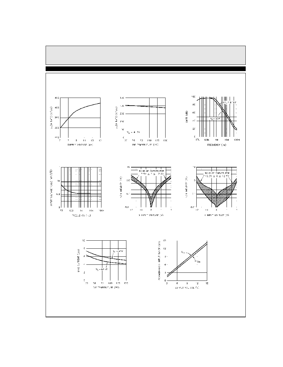
Slew Rate
vs Supply Voltage
Slew Rate
vs Die Temperature
CMRR vs Frequency
Input Voltage Noise
vs Frequency
Nonlinearity of X Input
Nonlinearity of Y Input
Bias Current
vs Die Temperature
Common-Mode Input Range
vs Supply Voltage
D44450B.fm Page 5 Tuesday, April 21, 1998 9:51 AM