Äîêóìåíòàöèÿ è îïèñàíèÿ www.docs.chipfind.ru
GP1200ESM33
Caution: This device is sensitive to electrostatic discharge. Users should follow ESD handling procedures.
1/9
www.dynexsemi.com
FEATURES
s
High Thermal Cycling Capability
s
Non Punch Through Silicon
s
Isolated MMC Base with AlN Substrates
APPLICATIONS
s
High Reliability Inverters
s
Motor Controllers
s
Traction Drives
s
Resonant Converters
The Powerline range of high power modules includes dual
and single switch configurations covering voltages from 1200V to
3300V and currents up to 4800A.
The GP1200ESM33 is a single switch 3300V, n channel
enhancement mode, insulated gate bipolar transistor (IGBT)
module. The IGBT has a wide reverse bias safe operating area
(RBSOA) ensuring reliability in demanding applications. This
device is optimised for traction drives and other applications
requiring high thermal cycling capability or very high reliability.
The module incorporates an electrically isolated base plate
and low inductance construction enabling circuit designers to
optimise circuit layouts and utilise grounded heat sinks for safety.
ORDERING INFORMATION
Order As:
GP1200ESM33
Note: When ordering, please use the whole part number.
KEY PARAMETERS
V
CES
3300V
V
CE(sat)
(typ)
3.4V
I
C
(max)
1200A
I
C(PK)
(max)
2400A
GP1200ESM33
High Reliability Single Switch IGBT Module
Advance Information
Replaces July 2000 version, DS5308-1.6
DS5308-2.1 February 2001
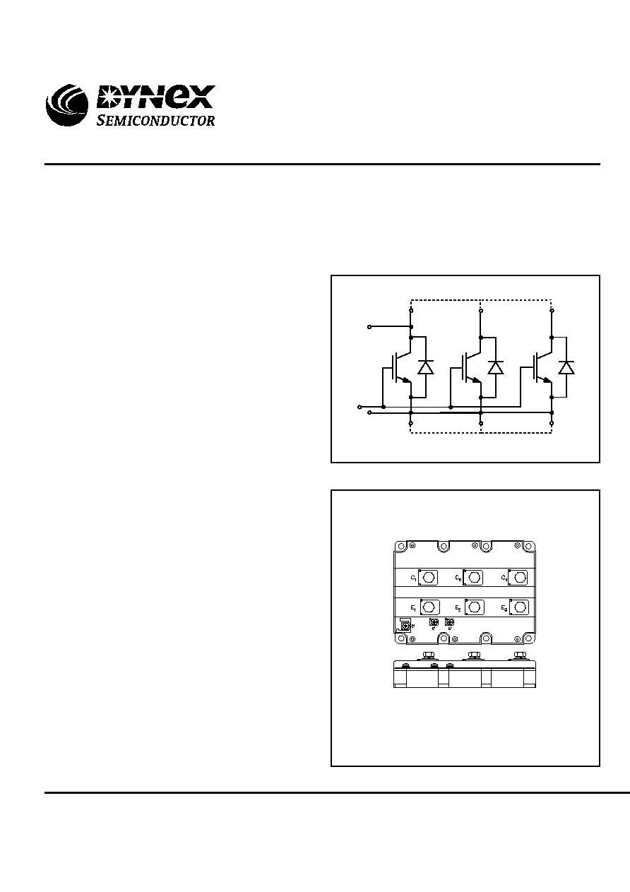
Fig. 1 Single switch circuit diagram
Fig. 2 Electrical connections - (not to scale)
Outline type code: E
(See package details for further information)
C2
C1
Aux C
G
Aux E
E1
E2
E3
External connection
External connection
C3

GP1200ESM33
2/9
Caution: This device is sensitive to electrostatic discharge. Users should follow ESD handling procedures.
www.dynexsemi.com
Test Conditions
Continuous dissipation -
junction to case
Continuous dissipation -
junction to case
Mounting torque 5Nm
(with mounting grease)
Transistor
Diode
-
Mounting - M6
Electrical connections - M4
Electrical connections - M8
Parameter
Thermal resistance - transistor
Thermal resistance - diode
Thermal resistance - case to heatsink (per module)
Junction temperature
Storage temperature range
Screw torque
THERMAL AND MECHANICAL RATINGS
ABSOLUTE MAXIMUM RATINGS
Stresses above those listed under 'Absolute Maximum Ratings' may cause permanent damage to the device. In extreme
conditions, as with all semiconductors, this may include potentially hazardous rupture of the package. Appropriate safety
precautions should always be followed. Exposure to Absolute Maximum Ratings may affect device reliability.
T
case
= 25°C unless stated otherwise
Symbol
V
CES
V
GES
I
C
I
C(PK)
P
max
V
isol
Test Conditions
V
GE
= 0V
-
T
case
= 80°C
1ms, T
case
= 120°C
T
case
= 25°C, T
j
= 150°C
Commoned terminals to base plate. AC RMS, 1 min, 50Hz
Units
V
V
A
A
kW
V
Max.
3300
±
20
1200
2400
14.7
6000
Parameter
Collector-emitter voltage
Gate-emitter voltage
Continuous collector current
Peak collector current
Max. transistor power dissipation
Isolation voltage
Symbol
R
th(j-c)
R
th(j-c)
R
th(c-h)
T
j
T
stg
-
Units
°C/kW
°C/kW
°C/kW
°C
°C
°C
Nm
Nm
Nm
Max.
8.5
16.3
4
125
125
125
5
2
10
Min.
-
-
-
-
-
40
-
-
-

GP1200ESM33
Caution: This device is sensitive to electrostatic discharge. Users should follow ESD handling procedures.
3/9
www.dynexsemi.com
Test Conditions
V
GE
= 0V, V
CE
= V
CES
V
GE
= 0V, V
CE
= V
CES
, T
case
= 125°C
V
GE
=
±
20V, V
CE
= 0V
I
C
= 120mA, V
GE
= V
CE
V
GE
= 15V, I
C
= 1200A
V
GE
= 15V, I
C
= 1200A, , T
case
= 125°C
DC
t
p
= 1ms
I
F
= 1200A
I
F
= 1200A, T
case
= 125°C
V
CE
= 25V, V
GE
= 0V, f = 1MHz
-
Parameter
Collector cut-off current
Gate leakage current
Gate threshold voltage
Collector-emitter saturation voltage
Diode forward current
Diode maximum forward current
Diode forward voltage
Input capacitance
Module inductance
ELECTRICAL CHARACTERISTICS
T
case
= 25°C unless stated otherwise.
Symbol
I
CES
I
GES
V
GE(TH)
V
CE(sat)
I
F
I
FM
V
F
C
ies
L
M
Units
mA
mA
µ
A
V
V
V
A
A
V
V
nF
nH
Max.
3
100
12
6.5
4.3
5
1200
2400
2.9
3
-
-
Typ.
-
-
-
5.5
3.4
4.3
-
-
2.3
2.4
300
10
Min.
-
-
-
4.5
-
-
-
-
-
-
-
-

GP1200ESM33
4/9
Caution: This device is sensitive to electrostatic discharge. Users should follow ESD handling procedures.
www.dynexsemi.com
Units
µ
s
µ
s
J
µ
s
µ
s
J
µ
C
A
J
Max.
-
-
-
-
-
-
-
-
-
Typ.
3.2
0.9
1.6
1.1
0.4
1.6
600
1200
0.7
Min.
-
-
-
-
-
-
-
-
-
Test Conditions
I
C
= 1200A
V
GE
=
±
15V
V
CE
= 1800V
R
G(ON)
= 1.8
, R
G(OFF)
= 3.3
C
GE
= 660nF,
L ~ 90nH
I
F
= 1200A, V
R
= 1800V,
dI
F
/dt = 5500A/
µ
s
Parameter
Turn-off delay time
Fall time
Turn-off energy loss
Turn-on delay time
Rise time
Turn-on energy loss
Diode reverse recovery charge
Diode reverse current
Diode reverse recovery energy
ELECTRICAL CHARACTERISTICS
T
case
= 25°C unless stated otherwise
Symbol
t
d(off)
t
f
E
OFF
t
d(on)
t
r
E
ON
Q
rr
I
rr
E
REC
T
case
= 125°C unless stated otherwise
Units
µ
s
µ
s
J
µ
s
µ
s
J
µ
C
A
J
Max.
-
-
-
-
-
-
-
-
-
Typ.
3.4
1.5
2.4
1.1
0.5
2.3
1000
1300
1.1
Min.
-
-
-
-
-
-
-
-
-
Test Conditions
I
C
= 1200A
V
GE
=
±
15V
V
CE
= 1800V
R
G(ON)
= 1.8
, R
G(OFF)
= 3.3
C
GE
= 660nF,
L ~ 90nH
I
F
= 1200A, V
R
= 1800V,
dI
F
/dt = 4500A/
µ
s
Parameter
Turn-off delay time
Fall time
Turn-off energy loss
Turn-on delay time
Rise time
Turn-on energy loss
Diode reverse recovery charge
Diode reverse current
Diode reverse recovery energy
Symbol
t
d(off)
t
f
E
OFF
t
d(on)
t
r
E
ON
Q
rr
I
rr
E
REC
GP1200ESM33
Caution: This device is sensitive to electrostatic discharge. Users should follow ESD handling procedures.
5/9
www.dynexsemi.com
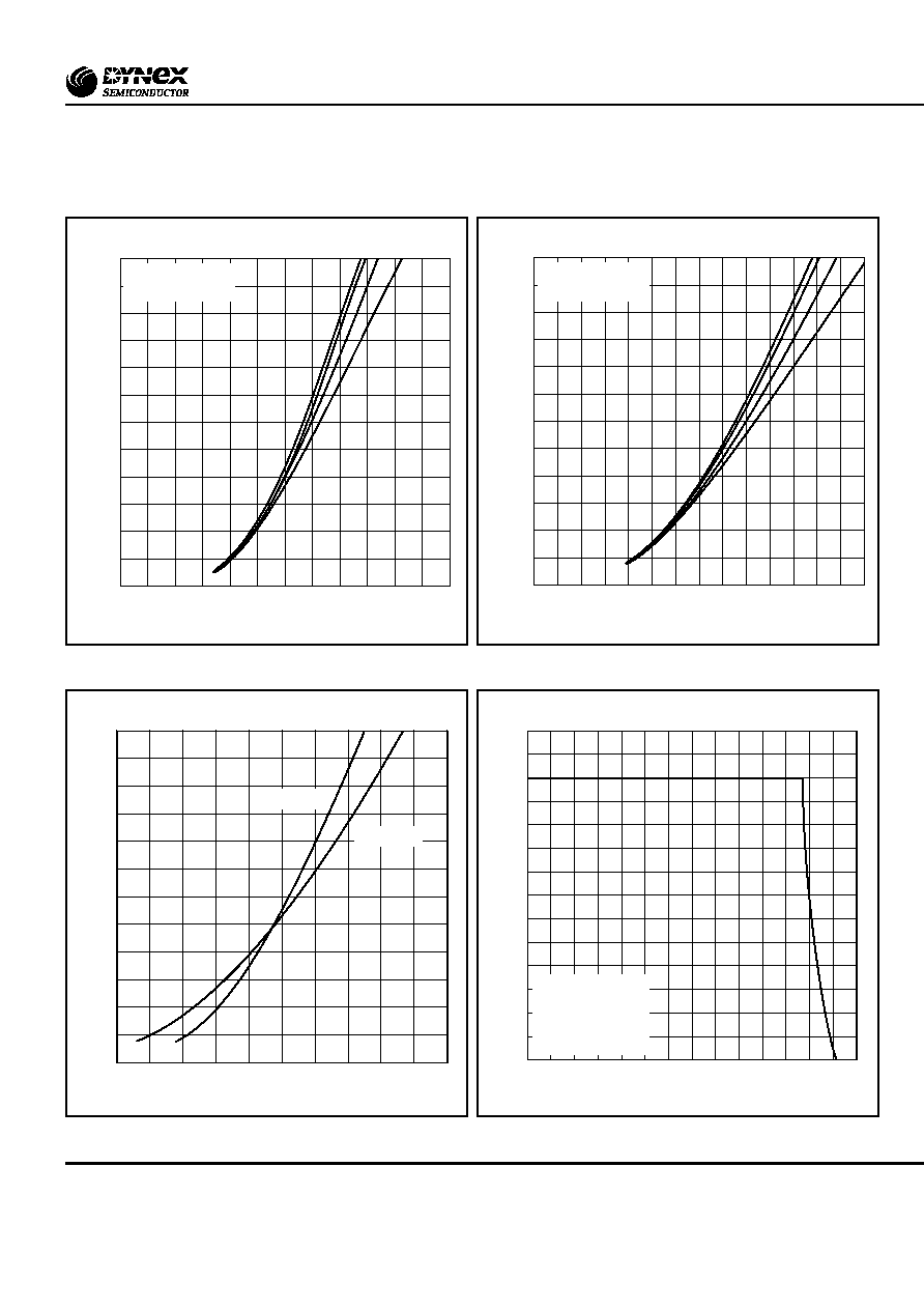
TYPICAL CHARACTERISTICS
Fig.3 Typical output characteristics
Fig.4 Typical output characteristics
Fig.5 Diode typical forward characteristics
Fig.6 Reverse bias safe operating area
0
1000
1200
1400
2000
2200
2400
0
1.0
2.0
3.0
4.0
5.0
6.0
Collector-emitter voltage, V
ce
- (V)
Collector current, I
c
- (A)
V
ge
= 20/15/12/10V
Common emitter
T
case
= 25°C
1800
1600
200
400
600
800
0
1000
1200
1400
2000
2200
2400
0
1.0
2.0
3.0
4.0
5.0
6.0
7.0
Collector-emitter voltage, V
ce
- (V)
Collector current, I
c
- (A)
V
ge
= 20/15/12/10V
Common emitter
T
case
= 125°C
1800
1600
200
400
600
800
0
1000
1200
1400
400
200
600
800
1600
1800
2000
2200
2400
1.0
1.5
2.0
2.5
3.0
3.5
Foward voltage, V
F
- (V)
Foward current, I
F
- (A)
T
j
= 125°C
T
j
= 25°C
0
600
800
200
400
1000
1200
1400
1600
1800
2000
2200
2400
2600
2800
0
500
1000
1500
2000
2500
3000
3500
Collector-emitter voltage, V
ce
- (V)
Collector current, I
C
- (A)
T
case
= 125°C
V
ge
= ±15V
R
g(OFF)
= 3.3
C
GE
= 660nF
dV
CE
/dt < 9000V/µs