1
) Mounted on P.C. board with 3 mm
2
copper pad at each terminal
Montage auf Leiterplatte mit 3 mm
2
Kupferbelag (Lötpad) an jedem Anschluß
42
01.11.2003
2.
5
ma
x
1.
3
±0
.
1
1.1
2.9
±0.1
0.4
1
2
3
Type
Code
1.9
BCW 65, BCW 66
General Purpose Transistors
NPN
Surface mount Si-Epitaxial PlanarTransistors
Si-Epitaxial PlanarTransistoren für die Oberflächenmontage
NPN
Power dissipation Verlustleistung
250 mW
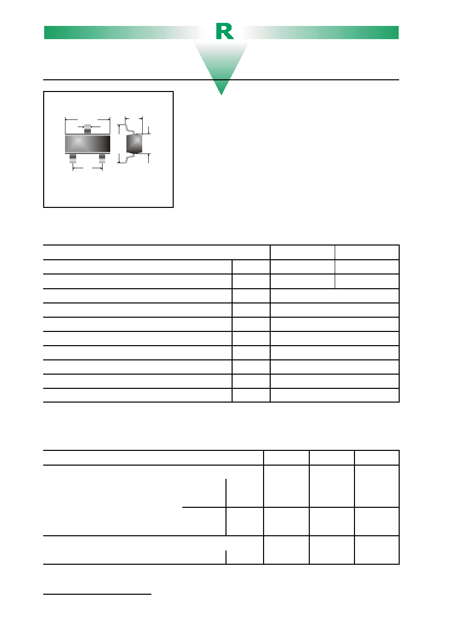
Plastic case
SOT-23
Kunststoffgehäuse
(TO-236)
Weight approx. Gewicht ca.
0.01 g
Plastic material has UL classification 94V-0
Gehäusematerial UL94V-0 klassifiziert
Dimensions / Maße in mm
1 = B
2 = E
3 = C
Standard packaging taped and reeled
Standard Lieferform gegurtet auf Rolle
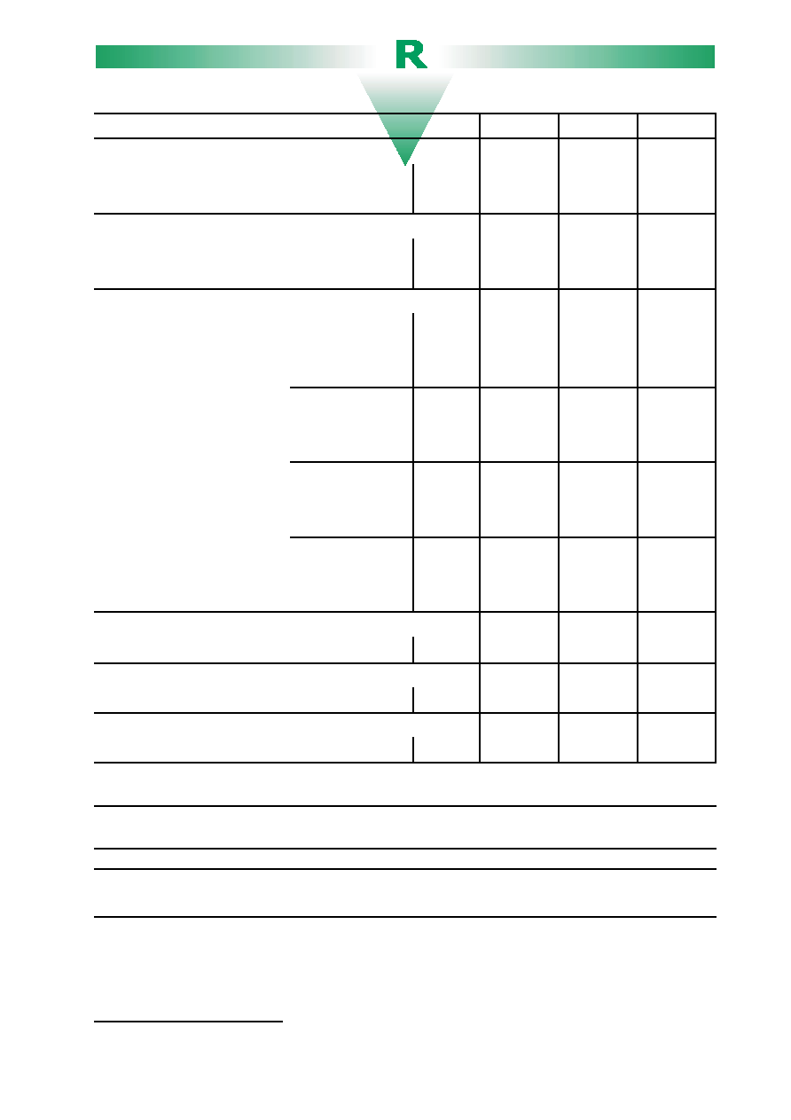
Maximum ratings (T
A
= 25
/
C)
Grenzwerte (T
A
= 25
/
C)
BCW 65
BCW 66
Collector-Emitter-voltage
B open
V
CE0
32 V
45 V
Collector-Base-voltage
E open
V
CB0
60 V
75 V
Emitter-Base-voltage
C open
V
EB0
5 V
Power dissipation Verlustleistung
P
tot
250 mW
1
)
Collector current Kollektorstrom (DC)
I
C
800 mA
Peak Collector current Kollektor-Spitzenstrom
I
CM
1000 mA
Base current Basis-Spitzenstrom
I
B
100 mA
Peak Base current Basis-Spitzenstrom
I
BM
200 mA
Junction temperature Sperrschichttemperatur
T
j
150
/
C
Storage temperature Lagerungstemperatur
T
S
- 65...+ 150
/
C
Characteristics (T
j
= 25
/
C)
Kennwerte (T
j
= 25
/
C)
Min.
Typ.
Max.
Collector-Base cutoff current Kollektorreststrom
I
E
= 0, V
CB
= 32 V
BCW 65
I
CB0
20 nA
I
E
= 0, V
CB
= 32 V, T
j
= 150
/
C
I
CB0
20
:
A
I
E
= 0, V
CB
= 45 V
BCW 66
I
CB0
20 nA
I
E
= 0, V
CB
= 45 V, T
j
= 150
/
C
I
CB0
20
:
A
Emitter-Base cutoff current Emitterreststrom
I
C
= 0, V
EB
= 4 V
I
EB0
20 nA
1
) Tested with pulses t
p
= 300
:
s, duty cycle
#
2% Gemessen mit Impulsen t
p
= 300
:
s, Schaltverhältnis
#
2%
2
) Mounted on P.C. board with 3 mm
2
copper pad at each terminal
Montage auf Leiterplatte mit 3 mm
2
Kupferbelag (Lötpad) an jedem Anschluß
43
01.11.2003
General Purpose Transistors
BCW 65, BCW 66
Characteristics (T
j
= 25
/
C)
Kennwerte (T
j
= 25
/
C)
Min.
Typ.
Max.
Collector saturation volt. Kollektor-Sättigungsspg.
1
)
I
C
= 100 mA, I
B
= 10 mA
V
CEsat
300 mV
I
C
= 500 mA, I
B
= 50 mA
V
CEsat
700 mV
Base saturation voltage Basis-Sättigungsspannung
1
)
I
C
= 100 mA, I
B
= 10 mA
V
BEsat
1.25 V
I
C
= 500 mA, I
B
= 50 mA
V
BEsat
2 V
DC current gain Kollektor-Basis-Stromverhältnis
1
)
V
CE
= 10 V, I
C
= 100
:
A
BCW 65A / 66F
h
FE
35
BCW 65B / 66G
h
FE
50
BCW 65C / 66H
h
FE
80
V
CE
= 1 V, I
C
= 10 mA
BCW 65A / 66F
h
FE
75
BCW 65B / 66G
h
FE
110
BCW 65C / 66H
h
FE
180
V
CE
= 1 V, I
C
= 100 mA
BCW 65A / 66F
h
FE
100
160
250
BCW 65B / 66G
h
FE
160
250
400
BCW 65C / 66H
h
FE
250
350
630
V
CE
= 2 V, I
C
= 500 mA
BCW 65A / 66F
h
FE
35
BCW 65B / 66G
h
FE
60
BCW 65C / 66H
h
FE
100
Gain-Bandwidth Product Transitfrequenz
V
CE
= 5 V, I
C
= 50 mA, f = 100 MHz
f
T
170 MHz
Collector-Base Capacitance Kollektor-Basis-Kapazität
V
CB
= 10 V, I
E
= i
e
= 0, f = 1 MHz
C
CB0
6 pF
Emitter-Base Capacitance Emitter-Basis-Kapazität
V
EB
= 0.5 V, I
C
= i
c
= 0, f = 1 MHz
C
EB0
60 pF
Thermal resistance junction to ambient air
Wärmewiderstand Sperrschicht umgebende Luft
R
thA
420 K/W
2
)
Recommended complementary PNP transistors
Empfohlene komplementäre PNP-Transistoren
BCW 67, BCW 68
Marking Stempelung
BCW 65A = EA
BCW 65B = EB
BCW 65C = EC
BCW 66F = EF
BCW 66G = EG
BCW 66H = EH