
B
C
D
E
G
H
J
K
L
M
A
P
1
2
3
4
PIN 1
PIN 3
PIN 4
Note:
Pins 1 & 3 must be electrically
connected at the printed circuit board.
DS30202 Rev. E-1
1 of 2
SBD835L
SBD835L
8A SURFACE MOUNT SCHOTTKY BARRIER RECTIFIER
Features
Single phase, half wave, 60Hz, resistive or inductive load.
For capacitive load, derate current by 20%.
Maximum Ratings and Electrical Characteristics
@ T
A
= 25°C unless otherwise specified
·
Case: DPAK Molded Plastic
·
Terminals: Solderable per MIL-STD-202,
Method 208
·
Polarity: See Diagram
·
Marking: Type Number
·
Weight: 0.4 grams (approx.)
Mechanical Data
DPAK
Dim
MinMax
A
6.3
6.7
B
ľ
10
C
0.3
0.8
D
2.3 Nominal
E
2.1
2.5
G
0.4
0.6
H
1.2
1.6
J
5.3
5.7
K
0.5 Nominal
L
1.3
1.8
M
1.0
ľ
P
5.1
5.5
All Dimensions in mm
Characteristic
Symbol
SBD835L
Unit
Peak Repetitive Reverse Voltage
Working Peak Reverse Voltage
DC Blocking Voltage
V
RRM
V
RWM
V
R
35
V
RMS Reverse Voltage
V
R(RMS)
25
V
Average Rectified Output Current
@ T
C
= 88°C
I
O
8
A
Non-Repetitive Peak Forward Surge Current
8.3ms Single half sine-wave Superimposed on Rated Load
(JEDEC Method)
I
FSM
150
A
Forward Voltage (Note 2)
@ I
F
= 8A, T
j
= 25°C
@ I
F
= 8A, T
j
= 125°C
V
FM
0.51
0.41
V
Voltage Rate of Change
dv/dt
10,000
V/ms
Peak Reverse Current
@ T
C
= 25°C
at Rated DC Blocking Voltage
@ T
C
= 100°C
I
RM
1.4
35
mA
Typical Junction Capacitance (Note 3)
C
J
300
pF
Typical Thermal Resistance Junction to Case (Note 1)
R
qJC
6
°C/W
Typical Thermal Resistance Junction to Ambient
R
qJA
80
°C/W
Operating Temperature Range
T
j
-65 to +125
°C
Storage Temperature Range
T
STG
-65 to +150
°C
·
Guard Ring Die Construction for
Transient Protection
·
Low Power Loss, High Efficiency
·
High Surge Capability
·
High Current Capability and Very Low
Forward Voltage Drop
·
Surge Overload Rating to 150A Peak
·
Plastic Material: UL Flammability
Classification Rating 94V-0
Notes:
1. Thermal resistance: junction to case, unit mounted on PC board with 5.0 mm
2
(0.013 mm thick) copper pad as heat sink.
2. 300ms pulse width, 2% duty cycle.
3. f = 1 MHz, V
R
= 5VDC.
ADVANCE
INFORMATION
DS30202 Rev. E-1
2 of 2
SBD835L
ADVANCE
INFORMATION
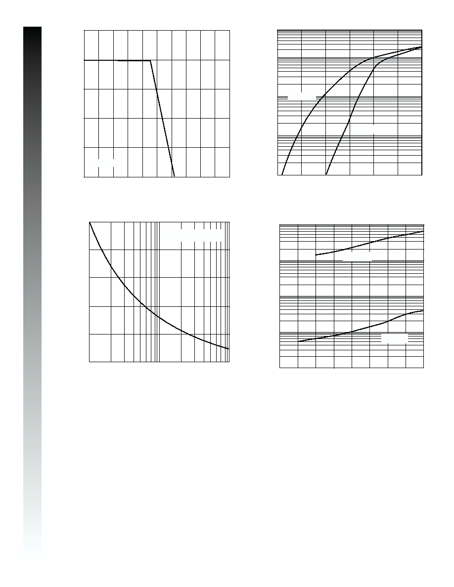
0
30
60
90
120
150
1
10
100
I
,
PEAK
F
O
R
W
ARD
SURGE
CURRENT
(A)
FSM
Number of Cycles at 60Hz
Fig. 3 Max Non-Repetitive Surge Current
8.3ms single Half-Sine-Wave
(JEDEC Method)
0
2
4
6
8
10
0
100
200
I
,
A
VERAGE
F
O
R
W
ARD
CURRENT
(A)
(A
V)
T , CASE TEMPERATURE (°C)
Fig. 1 Forward Current Derating Curve
C
T = 125şC
J
0.1
0.01
1
10
100
0
0.2
0.4
0.6
I
,
INST
ANT
ANEOUS
FWD
CURRENT
(A)
F
V , INSTANTANEOUS FORWARD VOLTAGE (V)
Fig. 2 Typical Fwd Characteristics per Element
F
0.1
0.3
0.5
T = 25şC
J
T = 125şC
J
0.001
0.01
0.1
1.0
10.0
0
I
,
INST
ANT
ANEOUS
REVERSE
CURRENT
(
A
)
R
m
V , RATED PEAK REVERSE VOLTAGE (V)
Fig. 4 Typical Reverse Characteristics
R
5
10
15
20
30
25
35
40
T = 25şC
J
T = 100şC
J