
DS23022 Rev. 4 - 2
1 of 3
SB120-SB160
www.diodes.com
SB120 - SB160
1.0A SCHOTTKY BARRIER RECTIFIER
Features
A
A
B
C
D
DO-41 Plastic
Dim
Min
Max
A
25.40
ľ
B
4.06
5.21
C
0.71
0.864
D
2.00
2.72
All Dimensions in mm
Maximum Ratings and Electrical Characteristics
@ T
A
= 25
°C unless otherwise specified
·
Schottky Barrier Chip
·
Guard Ring Die Construction for
Transient Protection
·
Low Power Loss, High Efficiency
·
High Surge Capability
·
High Current Capability and Low Forward
Voltage Drop
·
Surge Overload Rating to 40A Peak
·
For Use in Low Voltage, High Frequency
Inverters, Free Wheeling, and Polarity
Protection Applications
·
Plastic Material - UL Flammability
Classification 94V-0
Mechanical Data
·
Case: Molded Plastic
·
Terminals: Plated Leads Solderable per
MIL-STD-202, Method 208
·
Polarity: Cathode Band
·
Weight: 0.3 grams (approx.)
·
Mounting Position: Any
·
Marking: Type Number
Single phase, half wave, 60Hz, resistive or inductive load.
For capacitive load, derate current by 20%.
Characteristic
Symbol
SB120
SB130
SB140
SB150
SB160
Unit
Peak Repetitive Reverse Voltage
Working Peak Reverse Voltage
DC Blocking Voltage
V
RRM
V
RWM
V
R
20
30
40
50
60
V
RMS Reverse Voltage
V
R(RMS)
14
21
28
35
42
V
Average Rectified Output Current
(Note 1)
(See Figure 1)
I
O
1.0
A
Non-Repetitive Peak Forward Surge Current 8.3ms
single half sine-wave superimposed on rated load
(JEDEC Method)
I
FSM
40
A
Forward Voltage (Note 2)
@ I
F
= 1.0A
V
FM
0.50
0.70
V
Peak Reverse Current
@ T
A
= 25
°C
at Rated DC Blocking Voltage (Note 2)
@ T
A
= 100
°C
I
RM
0.5
mA
10
5.0
Typical Thermal Resistance Junction to Lead (Note 1)
R
qJL
15
°C/W
Typical Thermal Resistance Junction to Ambient
R
qJA
50
°C/W
Operating Temperature Range
T
j
-65 to +125
-65 to +150
°C
Storage Temperature Range
T
STG
-65 to +150
Notes:
1. Measured at ambient temperature at a distance of 9.5mm from the case.
2. Short duration test pulse used to minimize self-heating effect.
DS23022 Rev. 4 - 2
2 of 3
SB120-SB160
www.diodes.com
0.01
0.1
1.0
10
0
0.2
0.4
0.6
0.8
1.0
I
,
INST
ANT
A
NEOUS
FOR
W
A
RD
CURRENT
(A)
F
V , INSTANTANEOUS FWD VOLTAGE (V)
F
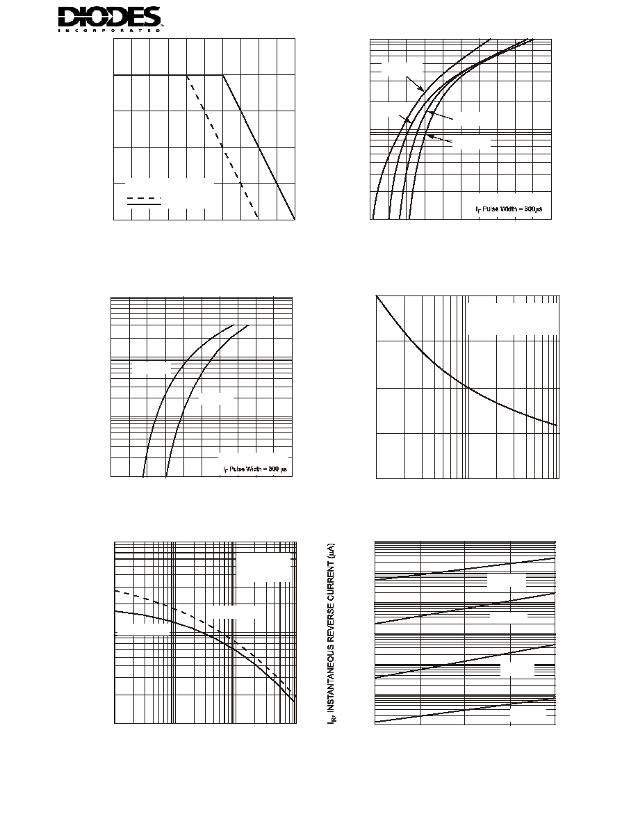
Fig. 3 Typ. Forward Characteristics - SB150 thru SB160
T = +125şC
j
T = +25şC
j
1% Duty Cycle
10
20
30
40
0
1
10
100
I
,
PEAK
FOR
W
ARD
S
URGE
C
URRENT
(A)
FSM
NUMBER OF CYCLES AT 60 Hz
Fig. 4 Max Non-Repetitive Peak Fwd Surge Current
8.3ms Single Half Sine-Wave
(JEDEC Method)
T = T
j
j(max)
10
100
1000
0.1
1
10
100
C
,
T
O
T
A
L
C
AP
ACIT
A
NCE
(pF)
T
V , REVERSE VOLTAGE (V)
R
Fig. 5 Typical Total Capacitance
SB150 - SB160
SB120 - SB140
T = 25
°C
j
f = 1.0MHz
V
= 50m Vp-p
sig
0.1
1.0
10
0.2
0.4
0.6
0.8
1.0
1.2
I
,
INST
ANT
A
NEOUS
FWD
CURRENT
(A)
F
V , INSTANTANEOUS FORWARD VOLTAGE (V)
F
Fig. 2 Typical Forward Characteristics - SB120 thru SB140
T = +25
°C
j
T = +75
°C
j
T = +125
°C
j
T = -25
°C
j
1% Duty Cycle
0
0.5
1.0
25
50
75
100
125
150
I
A
VERAGE
FOR
W
A
RD
CURRENT
(A)
(O),
T , LEAD TEMPERATURE (
°C)
L
Fig. 1 Forward Current Derating Curve
Resistive or Inductive Load
0.375" (9.5mm) lead length
SB120 - SB140
SB150 & SB160
100
10
1
0.1
0.01
1000
10,000
0
25
100
PERCENTAGE OF PEAK REVERSE VOLTAGE (%)
Fig. 6 Typical Reverse Characteristics, SB120 thru SB140
50
75
T = +25
°C
j
T = +125
°C
j
T = -25
°C
j
T = +75
°C
j
