e
3
DS30485 Rev. 8 - 2
1 of 3
PDS1040CTL
PowerDI is a trademark of Diodes Incorporated.
www.diodes.com
ă
Diodes Incorporated
PDS1040CTL
10A DUAL LOW VF SCHOTTKY BARRIER RECTIFIER
PowerDI
ä
5
Features
Single phase, half wave, 60Hz, resistive or inductive load.
For capacitive load, derate current by 20%.
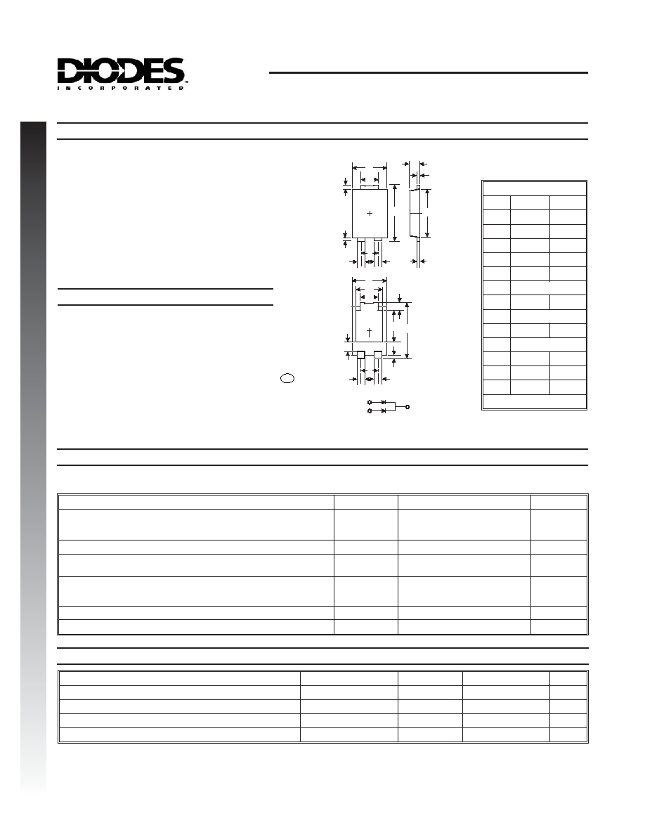
Mechanical Data
Characteristic
Symbol
Value
Unit
Peak Repetitive Reverse Voltage
Working Peak Reverse Voltage
DC Blocking Voltage
V
RRM
V
RWM
V
R
40
V
RMS Reverse Voltage
V
R(RMS)
28
V
Average Rectified Output Current (See also Figure 5) per element
total device
I
O
5
10
A
Non-Repetitive Peak Forward Surge Current
8.3ms Single half sine-wave Superimposed on Rated Load
Per element
I
FSM
110
A
Operating Temperature Range
T
j
-65 to +150
°C
Storage Temperature Range
T
STG
-65 to +150
°C
NEW
P
RODUCT
Maximum Ratings
@ T
A
= 25
°C unless otherwise specified
E
E1
b1
A
A2
A2
D
b2
b1
e
L1
L1
E
b1
D
b2
b1
e
D2
L
E2
L1
LEFT PIN
RIGHT PIN
TOP VIEW
BOTTOMSIDE
HEAT SINK
BOTTOMSIDE
HEAT SINK
W
PowerDI
ä
5
Dim
Min
Max
A
1.05
1.15
A2
0.33
0.43
b1
0.80
0.99
b2
1.70
1.88
D
3.90
4.05
D2
3.05 NOM
E
6.40
6.60
e
1.84 NOM
E1
5.30
5.45
E2
3.55 NOM
L
0.75
0.95
L1
0.50
0.65
W
1.20
1.50
All Dimensions in mm
Characteristic
Symbol
Typ
Max
Unit
Thermal Resistance Junction to Soldering Point
R
qJS
ľ
2.0
°C/W
Thermal Resistance Junction to Ambient Air (Note 2)
R
qJA
95
ľ
°C/W
Thermal Resistance Junction to Ambient Air (Note 3)
R
qJA
75
ľ
°C/W
Thermal Resistance Junction to Ambient Air (Note 4)
R
qJA
50
ľ
°C/W
Notes: 1. RoHS revision 13.2.2003. Glass and High Temperature Solder Exemptions Applied, see
EU Directive Annex Notes 5 and 7.
2. FR-4 PCB, 2 oz. Copper, minimum recommended pad layout per http://www.diodes.com/datasheets/ap02001.pdf.
3. Polyimide PCB, 2 oz. Copper, minimum recommended pad layout per http://www.diodes.com/datasheets/ap02001.pdf.
4. Polyimide PCB, 2 oz. Copper. Cathode pad dimensions 9.4mm x 7.2mm. Anode pad dimensions 2.7mm x 1.6mm.
Thermal Characteristics
@ T
A
= 25
°C unless otherwise specified
·
Case: PowerDI
ä
5
·
Case Material: Molded Plastic, "Green" Molding
Compound. UL Flammability Classification Rating 94V-0
·
Moisture Sensitivity: Level 1 per J-STD-020C
·
Terminals: Finish Matte Tin annealed over Copper
leadframe. Solderable per MIL-STD-202, Method 208
·
Polarity: See Diagram
·
Marking: See Page 3
·
Weight: 0.096 grams (approx.)
·
Guard Ring Die Construction for
Transient Protection
·
Low Power Loss, High Efficiency
·
Low Forward Voltage Drop
·
Very Low Reverse Leakage Current
·
For Use in Low Voltage, High Frequency Inverters, OR'ing,
and Polarity Protection Applications
·
High Forward Surge Current Capability
·
Lead Free Finish, RoHS Compliant (Note 1)
·
"Green" Molding Compound (No Br, Sb)
·
Qualified to AEC-Q101 Standards for High Reliability
SPICE MODEL: PDS1040CTL
DS30485 Rev. 8 - 2
2 of 3
PDS1040CTL
PowerDI is a trademark of Diodes Incorporated.
www.diodes.com
Characteristic
Symbol
Min
Typ
Max
Unit
Test Condition
Reverse Breakdown Voltage (Note 5)
V
(BR)R
40
ľ
ľ
V
I
R
= 500
mA
Forward Voltage Per Element
V
F
ľ
ľ
ľ
ľ
0.465
0.41
0.39
0.55
0.53
0.52
0.50
0.45
0.43
0.60
0.57
0.56
V
I
F
= 5A, Ts = 25
°C
I
F
= 5A, Ts = 100
°C
I
F
= 5A, Ts = 125
°C
I
F
= 10A, Ts = 25
°C
I
F
= 10A, Ts = 100
°C
I
F
= 10A, Ts = 125
°C
Reverse Leakage Current (Note 5) Per Element
I
R
ľ
ľ
ľ
ľ
ľ
ľ
20
3
15
2.5
6
1
200
25
150
10
80
5
mA
mA
mA
mA
mA
mA
V
R
= 40V, Ts = 25°C
V
R
= 40V, Ts = 100°C
V
R
= 35V, Ts = 25°C
V
R
= 35V, Ts = 100°C
V
R
= 17.5V, Ts = 25°C
V
R
= 17.5V, Ts = 100°C
Electrical Characteristics
@ T
A
= 25
°C unless otherwise specified
NEW
P
RODUCT
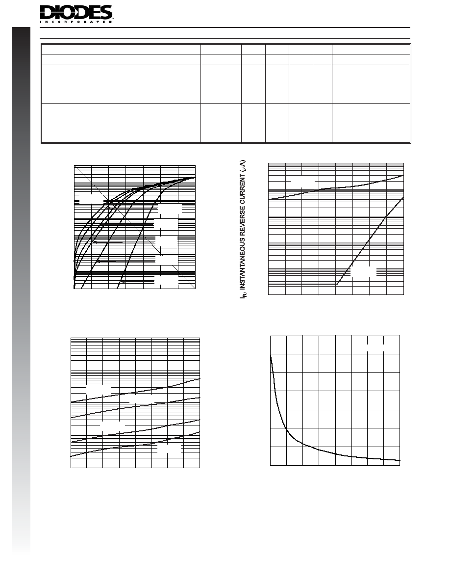
0
100
200
300
400
500
600
700
I
,
INST
ANT
A
NE
O
US
F
O
R
W
ARD
CURRENT
(A)
F
V , INSTANTANEOUS FORWARD VOLTAGE (mV)
Fig. 1 Typical Forward Characteristics, Per Element
F
0.00001
0.0001
0.001
0.01
0.1
1
10
100
T = 150°C
j
T = -65°C
j
T = 25°C
j
T = 85°C
j
T = 100°C
j
T = 125°C
j
0
5
10
15
20
25
30
40
35
V , INSTANTANEOUS REVERSE VOLTAGE (V)
Fig. 2 Typical Reverse Characteristics, Per Element
R
10
1
0.1
0.01
0.001
100
T = +25 C
j
°
T = -65°C
j
C
,
T
O
T
A
L
C
AP
ACIT
ANCE
(pF)
T
V , REVERSE VOLTAGE (V)
Fig. 4 Typical Total Capacitance vs. Reverse Voltage,
Per Element
R
100
200
300
400
500
600
700
800
0
5
10
15
20
25
30
35
40
f = 1 MHz
0
10
20
30
40
V , INSTANTANEOUS REVERSE VOLTAGE (V)
R
Fig. 3 Typical Reverse Characteristics, Per Element
I
,
INST
ANT
A
NE
O
US
REVERSE
CURRENT
(mA)
R
0.1
1
10
100
1,000
T = +125°C
j
T = +100°C
j
T = +150°C
j
T = +85°C
j
Notes:
5. Short duration test pulse used to minimize self-heating effect.
DS30485 Rev. 8 - 2
3 of 3
PDS1040CTL
PowerDI is a trademark of Diodes Incorporated.
www.diodes.com
NEW
P
RODUCT
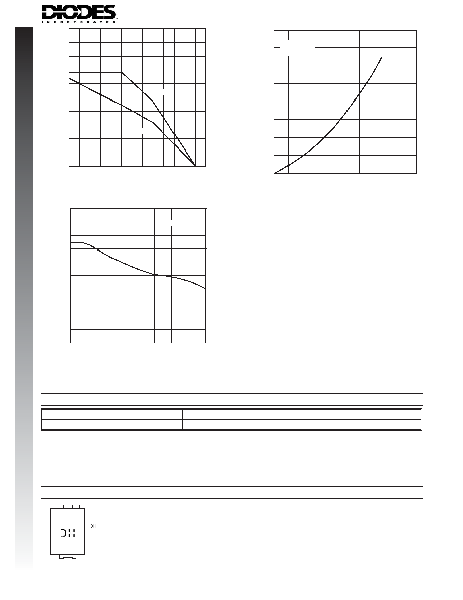
0
1.5
3.0
4.5
7.5
6.0
0
25
50
75
100
125
150
I,
D
C
F
O
R
W
ARD
C
URRENT
(A)
F
T , AMBIENT TEMPERATURE (°C)
Fig. 5 DC Forward Current Derating, Per Element
A
Note 2
Note 4
0
1
2
3
4
0
1
3
2
4
5
6
7
8
9
10
P
,
FOR
W
A
RD
POWER
D
ISSIP
A
TION
(W)
F
I , FORWARD CURRENT (A)
Fig. 6 Forward Power Dissipation, Per Element
F
I
PK
I
AV
= 1 (DC)
Ordering Information
Notes: 2. FR-4 PCB, 2 oz. Copper, minimum recommended pad layout per http://www.diodes.com/datasheets/ap02001.pdf.
3. Polyimide PCB, 2 oz. Copper, minimum recommended pad layout per http://www.diodes.com/datasheets/ap02001.pdf.
4. Polyimide PCB, 2 oz. Copper. Cathode pad dimensions 9.4mm x 7.2mm. Anode pad dimensions 2.7mm x 1.6mm.
5. Short duration test pulse used to minimize self-heating effect.
6. For Packaging Details, go to our website at http://www.diodes.com/datasheets/ap02007.pdf.
Device
Packaging
Shipping
PDS1040CTL-13
PowerDI
ä
5
5000/Tape & Reel
S1040CTL = Product type marking code
= Manufacturers' code marking
YYWW = Date code marking
YY = Last digit of year ex: 04 for 2004
WW = Week code 01 to 52
K = Factory Designator Code
YYWWK
S1040CTL
(Note 6)
0
40
200
160
120
80
0
10
20
30
40
T
,
DERA
TED
AMBIENT
T
EMPERA
T
URE
(°C)
A
V , DC REVERSE VOLTAGE (V)
Fig. 7 Operating Temperature Derating, Per Element
R
Note 2
Marking Information