DS30062 Rev. 4 - 2
1 of 2
MMBTA42
MMBTA42
NPN SMALL SIGNAL SURFACE MOUNT TRANSISTOR
·
Epitaxial Planar Die Construction
·
Complementary PNP Type Available
(MMBTA92)
·
Ideal for Medium Power Amplification and
Switching
Characteristic
Symbol
MMBTA42
Unit
Collector-Base Voltage
V
CBO
300
V
Collector-Emitter Voltage
V
CEO
300
V
Emitter-Base Voltage
V
EBO
6.0
V
Collector Current (Note 1) (Note 3)
I
C
500
mA
Power Dissipation (Note 1)
P
d
300
mW
Thermal Resistance, Junction to Ambient (Note 1)
R
qJA
417
K/W
Operating and Storage and Temperature Range
T
j
, T
STG
-55 to +150
°C
Features
Maximum Ratings
@ T
A
= 25
°C unless otherwise specified
A
E
J
L
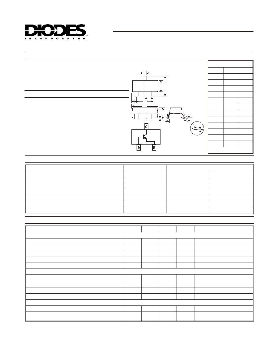
TOP VIEW
M
B C
C
B
H
G
D
K
E
Mechanical Data
·
Case: SOT-23, Molded Plastic
·
Case Material - UL Flammability Rating 94V-0
·
Moisture sensitivity: Level 1 per J-STD-020A
·
Terminals: Solderable per MIL-STD-202,
Method 208
·
Terminal Connections: See Diagram
·
Marking (See Page 2): K3M
·
Ordering & Date Code Information: See Page 2
·
Weight: 0.008 grams (approx.)
SOT-23
Dim
Min
Max
A
0.37
0.51
B
1.20
1.40
C
2.30
2.50
D
0.89
1.03
E
0.45
0.60
G
1.78
2.05
H
2.80
3.00
J
0.013
0.10
K
0.903
1.10
L
0.45
0.61
M
0.085
0.180
a
0
°
8
°
All Dimensions in mm
Notes:
1. Device mounted on FR-4 PCB, 1 inch x 0.85 inch x 0.062 inch; pad layout as shown on Diodes Inc. suggested pad layout
document AP02001, which can be found on our website at http://www.diodes.com/datasheets/ap02001.pdf.
2. Short duration test pulse used to minimize self-heating effect.
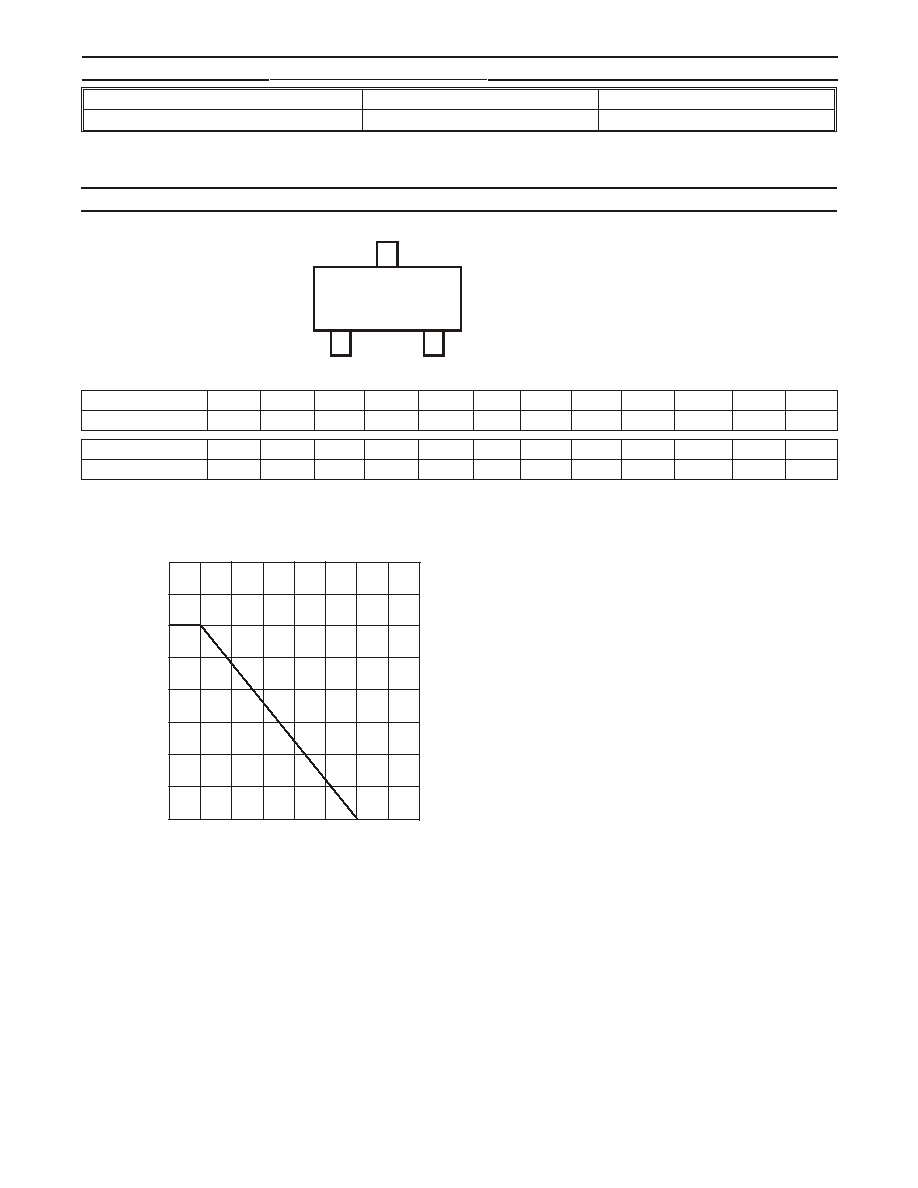
3. When operated under collector-emitter saturation conditions within the safe operating area defined by the thermal resistance
rating (R
qJA
), power dissipation rating (P
d
) and power derating curve (figure 1).
Electrical Characteristics
@ T
A
= 25
°C unless otherwise specified
Characteristic
Symbol
Min
Max
Unit
Test Condition
OFF CHARACTERISTICS (Note 2)
Collector-Base Breakdown Voltage
V
(BR)CBO
300
ľ
V
I
C
= 100
mA, I
E
= 0
Collector-Emitter Breakdown Voltage
V
(BR)CEO
300
ľ
V
I
C
= 1.0mA, I
B
= 0
Emitter-Base Breakdown Voltage
V
(BR)EBO
6.0
ľ
V
I
E
= 100
mA, I
C
= 0
Collector Cutoff Current
I
CBO
ľ
100
nA
V
CB
= 200V, I
E
= 0
Collector Cutoff Current
I
EBO
ľ
100
nA
V
CE
= 6.0V, I
C
= 0
ON CHARACTERISTICS (Note 2)
DC Current Gain
h
FE
25
40
40
ľ
ľ
I
C
= 1.0mA, V
CE
= 10V
I
C
= 10mA, V
CE
= 10V
I
C
= 30mA, V
CE
= 10V
Collector-Emitter Saturation Voltage
V
CE(SAT)
ľ
0.5
V
I
C
= 20mA, I
B
= 2.0mA
Base- Emitter Saturation Voltage
V
BE(SAT)
ľ
0.9
V
I
C
= 20mA, I
B
= 2.0mA
SMALL SIGNAL CHARACTERISTICS
Output Capacitance
C
cb
ľ
3.0
pF
V
CB
= 20V, f = 1.0MHz, I
E
= 0
Current Gain-Bandwidth Product
f
T
50
ľ
MHz
V
CE
= 20V, I
C
= 10mA,
f = 100MHz
DS30062 Rev. 4 - 2
2 of 2
MMBTA42
Ordering Information
(Note 4)
Device
Packaging
Shipping
MMBTA42-7
SOT-23
3000/Tape & Reel
Notes:
4. For Packaging Details, go to our website at http://www.diodes.com/datasheets/ap02007.pdf.
Marking Information
K3M
YM
K3M = Product Type Marking Code
YM = Date Code Marking
Y = Year ex: N = 2002
M = Month ex: 9 = September
Date Code Key
Month
Jan
Feb
March
Apr
May
Jun
Jul
Aug
Sep
Oct
Nov
Dec
Code
1
2
3
4
5
6
7
8
9
O
N
D
Year
1998
1999
2000
2001
2002
2003
2004
2005
2006
2007
2008
2009
Code
J
K
L
M
N
P
R
S
T
U
V
W
0
50
100
25
50
75
100 125
150 175 200
P
,
POWER
D
ISSIP
A
TION
(mW)
D
T , AMBIENT TEMPERATURE (°C)
A
Fig. 1, Max Power Dissipation vs
Ambient Temperature
150
200
250
300
350
0