DS21203 Rev. F-2
1 of 2
KBP005G-KBP10G
Characteristic
Symbol
KBP
005G
KBP
01G
KBP
02G
KBP
04G
KBP
06G
KBP
08G
KBP
10G
Unit
Peak Repetitive Reverse Voltage
Working Peak Reverse Voltage
DC Blocking Voltage
V
RRM
V
RWM
V
R
50
100
200
400
600
800
1000
V
RMS Reverse Voltage
V
R(RMS)
35
70
140
280
420
560
700
V
Average Rectified Output Current
@ T
C
= 105°C
I
O
1.5
A
Non-Repetitive Peak Forward Surge Current, 8.3 ms single
half-sine-wave superimposed on rated load
(JEDEC method)
I
FSM
40
A
Forward Voltage per element
@ I
F
= 1.5A
V
FM
1.1
V
Peak Reverse Current
@T
C
= 25°C
at Rated DC Blocking Voltage
@ T
C
= 125°C
I
RM
5.0
500
µA
Typical Junction Capacitance per(Note 1)
C
j
20
pF
Typical Thermal Resistance, junction to case (Note 2)
R
qJC
18
°C/W
Operating and Storage Temperature Range
T
j
, T
STG
-65 to +150
°C
KBP005G - KBP10G
1.5A GLASS PASSIVATED BRIDGE RECTIFIER
Features
·
Case: Molded Plastic
·
Terminals: Plated Leads, Solderable per
MIL-STD-202, Method 208
·
Polarity: As Marked on Body
·
Approx. Weight: 1.52 grams
·
Mounting Position: Any
·
Marking: Type Number
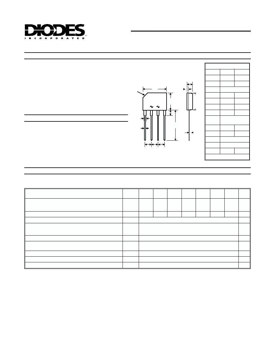
Mechanical Data
·
Glass Passivated Die Construction
·
High Case Dielectric Strength of 1500V
RMS
·
Low Reverse Leakage Current
·
Surge Overload Rating to 40A Peak
·
Ideal for Printed Circuit Board Applications
·
Plastic Material - UL Flammability
Classification 94V-0
·
UL Listed Under Recognized Component Index,
File Number E94661
Single phase, 60Hz, resistive or inductive load.
For capacitive load, derate current by 20%.
Maximum Ratings and Electrical Characteristics
@ T
A
= 25°C unless otherwise specified
C
E
G
H
J
K
L
M
N
P
+
_
A
B
D
KBP
Dim
Min
Max
A
14.25
14.75
B
10.20
10.60
C
2.29 Typical
D
14.25
14.73
E
3.56
4.06
G
0.76
0.86
H
1.17
1.42
J
2.8 X 45°
Chamfer
K
0.80
1.10
L
3.35
3.65
M
3° Nominal
N
2° Nominal
P
0.30
0.64
All Dimensions in mm
Notes:
1. Thermal resistance from junction to case per element. Unit mounted on 300 x 300 x 1.6mm aluminum plate heat sink.
2. Measured at 1.0 MHz and applied reverse voltage of 4.0V DC.

DS21203 Rev. F-2
2 of 2
KBP005G-KBP10G
0
0.1
1.0
10
0
0.2
0.4
0.6
0.8
1.0
1.2
1.4
I
,
INST
ANT
ANEOUS
FWD
CURRENT
(A)
F
V , INSTANTANEOUS FWD VOLTAGE (V)
Fig. 2 Typical Fwd Characteristics
F
T = 150°C
J
T = 25°C
J
Pulse Width
= 300 µs
0
10
20
30
40
50
1
10
100
I
,
PEAK
FWD
SURGE
CURRENT
(A)
FSM
NUMBER OF CYCLES AT 60 Hz
Fig. 3 Max Non-Repetitive Peak Fwd Surge Current
T = 150°c
Single Half
Sine Wave
(JEDEC Method)
j
1
10
100
1
10
100
C
,
CAP
ACIT
ANCE
(pF)
j
V , REVERSE VOLTAGE (V)
Fig. 4 Typical Junction Capacitance
R
T = 25°C
f = 1MHz
j
0.01
0.1
1.0
10
100
1000
10,000
0
20
40
60
80
100
120
140
I
,
INST
ANT
ANEOUS
REVERSE
CURRENT
(mA)
R
PERCENT OF RATED PEAK REVERSE VOLTAGE (%)
Fig. 5 Typical Reverse Characteristics
T = 125şC
j
T = 100şC
j
T = 25şC
j
T = 150şC
j
0
0.5
1.0
1.5
2.0
0
50
100
150
I
,
A
VERAGE
RECTIFIED
CURRENT
(A)
O
T, TEMPERATURE (°C)
Fig. 1 Forward Current Derating Curve
Ambient
Case
Lead