
DS21201 Rev. H-2
1 of 2
DF005M-DF10M
Characteristic
Symbol
DF
005M
DF
01M
DF
02M
DF
04M
DF
06M
DF
08M
DF
10M
Unit
Peak Repetitive Reverse Voltage
Working Peak Reverse Voltage
DC Blocking Voltage
V
RMM
V
RWM
V
R
50
100
200
400
600
800
1000
V
RMS Reverse Voltage
V
RMS
35
70
140
280
420
580
700
V
Average Rectified Output Current @ T
A
= 40°C
I
O
1.0
A
Non-Repetitive Peak Forward Surge Current, 8.3 ms
single half-sine-wave superimposed on rated load
(JEDEC method)
I
FSM
50
A
Forward Voltage (per element)
@ I
F
= 1.0 A
V
FM
1.1
V
Peak Reverse Current
@ T
A
= 25°C
at Rated DC Blocking Voltage (per element) @ T
A
= 125°C
I
RM
10
500
µA
I
2
t Rating for Fusing (t<8.3ms)
I
2
t
10.4
A
2
s
Typical Junction Capacitance per element (Note 1)
C
j
25
pF
Typical Thermal Resistance, Junction to Ambient (Note 2)
R
qJA
40
°C/W
Operating and Storage Temperature Range
T
j
, T
STG
-65 to +150
°C
DF005M - DF10M
1.0A GLASS PASSIVATED BRIDGE RECTIFIERS
Features
·
Case: Molded Plastic
·
Terminals: Solder Plated Leads,
Solderable per MIL-STD-202, Method 208
·
Polarity: As Marked on Case
·
Approx. Weight: 0.38 grams
·
Mounting Position: Any
·
Marking: Type Number
Mechanical Data
Notes:
1. Measured at 1.0MHz and Applied Reverse Voltage of 4.0V DC.
2. Thermal Resistance, junction to ambient, measured on PC board with 5.0
2
mm (0.03mm thick) land areas.
·
Glass Passivated Die Construction
·
Diffused Junction
·
Low Forward Voltage Drop, High Current
Capability
·
Surge Overload Rating to 50A Peak
·
Designed for Printed Circuit Board Applications
·
Plastic Material - UL Flammability
Classification 94V-0
·
UL Listed Under Recognized Component Index,
File Number E94661
Single phase, 60Hz, resistive or inductive load.
For capacitive load, derate current by 20%.
Maximum Ratings and Electrical Characteristics
@ T
A
= 25°C unless otherwise specified
DF-M
Dim
Min
Max
A
7.40
7.90
B
6.20
6.50
C
0.22
0.30
D
1.27
2.03
E
7.60
8.90
G
3.81
4.69
H
8.13
8.51
J
2.40
2.60
K
5.00
5.20
L
0.46
0.58
All Dimensions in mm
E
H
L
K
A
D
C
G
B
J
DS21201 Rev. H-2
2 of 2
DF005M-DF10M
0.01
0.1
1.0
10
0.4
0.6
0.8
1.0
1.2
1.4
I
,
INST
ANT
ANEOUS
FOR
W
ARD
CURRENT
(A)
F
V , INSTANTANEOUS FORWARD VOLTAGE (V)
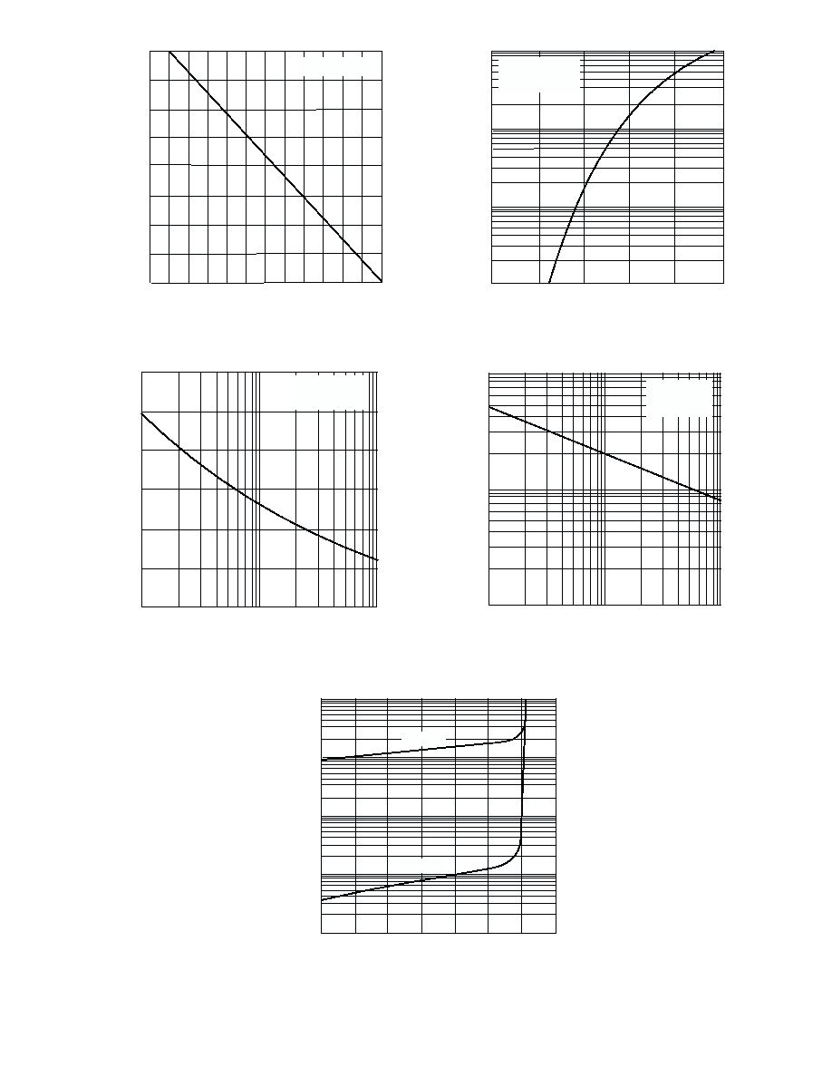
Fig. 2 Typ Forward Characteristics (per element)
F
T = 25°C
Pulse Width = 300µs
2% duty cycle
j
0
10
20
30
40
50
60
1
10
100
I
,
PEAK
FOR
W
ARD
SURGE
CURRENT
(A)
FSM
NUMBER OF CYCLES AT 60 Hz
Fig. 3 Max Non-Repetitive Peak Forward Surge Current
Single half-sine-Wave
(JEDEC Method)
1
10
100
1
10
100
C
,
CAP
ACIT
ANCE
(pF)
J
V , REVERSE VOLTAGE (V)
Fig. 4 Typ Junction Capacitance (per element)
R
T = 25°c
f = 1.0 Mhz
V = 50 mV p-p
j
sig
0.01
0.1
1.0
10
100
20
0
40
60
80
100
120
140
I
,
INST
ANT
ANEOUS
REVERSE
CURRENT
(µA)
R
PERCENT OF RATED PEAK REVERSE VOLTAGE (%)
Fig. 5 Typ Reverse Characteristics (per element)
T = 125°C
j
T = 25°C
j
1.0
0.5
0
40
60
80
100
120
140
I
,
A
VERAGE
FOR
W
ARD
CURRENT
(A)
(A
V)
T , AMBIENT TEMPERATURE (°C)
Fig. 1 Output Current Derating Curve
A
60 Hz Resistive or
Inductive load