Äîêóìåíòàöèÿ è îïèñàíèÿ www.docs.chipfind.ru
General Description
The DS4301 is a single 32-position linear digital poten-
tiometer with 200k
end-to-end resistance. The wiper
setting is stored in EEPROM, so the DS4301 powers up
with the last stored setting. The position of the wiper is
controlled through a simple three-terminal
increment/decrement interface. The DS4301 is ideal for
white LED backlight brightness control. Its 8-pin µSOP
package, 2.4V to 5.5V supply range, and 200k
end-
to-end resistance are especially suited for portable,
battery-powered applications such as cellular tele-
phones and PDAs.
Applications
White LED Backlight Brightness Control
Portable Battery-Powered Devices such as PDAs
and Cellular Phones
Any Application that Requires a Small, Low-Cost
NV Potentiometer
Features
Single, 32-Position, 200k Linear Nonvolatile (NV)
Potentiometer Ideal for Battery-Powered
Applications
Three-Terminal Increment/Decrement Interface to
Adjust Wiper Position
Wide Voltage Supply Range (2.4V to 5.5V)
Command-Initiated NV Wiper Storage
Operates Over the Industrial Temperature Range
(-40°C to +85°C)
Available in 8-Pin µSOP
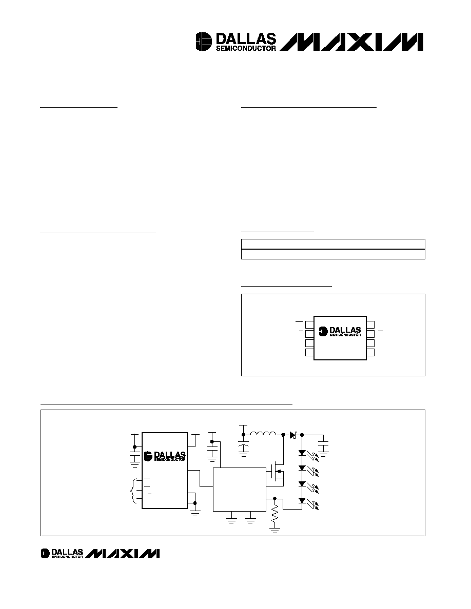
DS4301
Nonvolatile, 32-Position Digital Potentiometer
______________________________________________ Maxim Integrated Products
1
1
2
3
4
8
7
6
5
V
CC
CS
L
W
GND
H
U/D
INC
µSOP
TOP VIEW
DS4301
Pin Configuration
Ordering Information
V
CC
V
CC
V
CC
V
CC
V
REF
V
CC
ADJ
EXT
CS
FB
GND
PGND
W
H
L
WHITE LED
CURRENT
REGULATOR
R
FB
WHITE
LEDs
10
µH
MBR0540
1
µF
1
µF
10
µF
GND
CS
INC
U/D
0.1
µF
CONTROL
INTERFACE
DS4301
Typical Operating Circuit
Rev 0; 8/03
For pricing, delivery, and ordering information, please contact Maxim/Dallas Direct! at
1-888-629-4642, or visit Maxim's website at www.maxim-ic.com.
PART
TEMP RANGE
PIN-PACKAGE
DS4301U-200
-40°C to +85°C
8 µSOP (118 mil)
DS4301
Nonvolatile, 32-Position Digital Potentiometer
2
_____________________________________________________________________
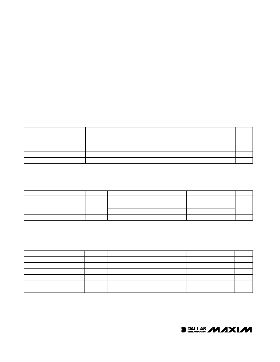
ABSOLUTE MAXIMUM RATINGS
RECOMMENDED DC OPERATION CONDITIONS
(V
CC
= V
CC MIN
to V
CC MAX
; T
A
= -40°C to +85°C, unless otherwise specified.)
Stresses beyond those listed under "Absolute Maximum Ratings" may cause permanent damage to the device. These are stress ratings only, and functional
operation of the device at these or any other conditions beyond those indicated in the operational sections of the specifications is not implied. Exposure to
absolute maximum rating conditions for extended periods may affect device reliability.
Voltage Range on V
CC
Pin Relative to Ground .....-0.5V to +6.0V
Voltage Range on CS, INC, U/D, L, W, H Pins
Relative to Ground*.....................................-0.5V to V
CC
+ 0.5V
Wiper Current .....................................................................±3mA
Operating Temperature Range ...........................-40°C to +85°C
Programming Temperature.....................................0°C to +70°C
Storage Temperature Range .............................-55°C to +125°C
Soldering Temperature .......................................See IPC/JEDEC
J-STD-020A Specification
*Not to exceed 6.0V
PARAMETER
SYMBOL
CONDITIONS
MIN
TYP
MAX
UNITS
Supply Voltage
V
CC
(Note 1)
+2.4
+5.5
V
Input Logic 1 (CS, INC, U/D)
V
IH
0.7 x V
CC
V
CC
+ 0.3
V
Input Logic 0 (CS, INC, U/D)
V
IL
-0.3
+0.3 x V
CC
V
Resistor Inputs
L, H, W
-0.3
V
CC
+ 0.3
V
Wiper Current
I
W
-1
+1
mA
DC ELECTRICAL CHARACTERISTICS
(V
CC
= V
CC MIN
to V
CC MAX
; T
A
= -40°C to +85°C, unless otherwise specified.)
PARAMETER
SYMBOL
CONDITIONS
MIN
TYP
MAX
UNITS
Input Leakage
I
L
-1
+1
µA
3V
30
60
Standby Current (Note 2)
I
STBY
5V
15
60
µA
Digital Input Capacitance
C
I/O
10
pF
ANALOG RESISTOR CHARACTERISTICS
(V
CC
= V
CC MIN
to V
CC MAX
; T
A
= -40°C to +85°C, unless otherwise specified.)
PARAMETER
SYMBOL
CONDITIONS
MIN
TYP
MAX
UNITS
End-to-End Resistor Tolerance
T
A
= +25°C
-20
+20
%
Wiper Resistance
R
W
500
2000
Absolute Linearity
(Note 3)
-0.5
+0.5
LSB
Relative Linearity
(Note 4)
-0.25
+0.25
LSB
End-to-End Temp Coefficient
-250
+250
ppm/°C
Ratiometric Temp Coefficient
7
ppm/°C
DS4301
Nonvolatile, 32-Position Digital Potentiometer
_____________________________________________________________________
3
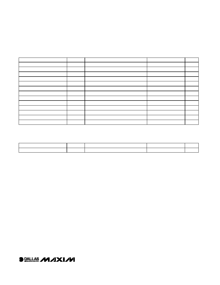
Note 1:
All voltages are referenced to ground.
Note 2:
STBY
specified for V
CC
equal to 3.0V and 5.0V while control port logic pins are driven to V
CC
or GND.
Note 3:
Absolute linearity is used to determine wiper voltage versus expected voltage as determined by wiper position.
Note 4:
Relative linearity is used to determine the change of wiper voltage between two adjacent wiper positions.
Note 5:
The INC low to CS inactive time is the transition time that allows the three control pins to become inactive without writing
the wiper position to the EEPROM.
Note 6:
Wiper storage time is the time required for the wiper position to be written to the EEPROM. During this time, the three-ter-
minal interface is inactive.
Note 7:
Wiper load time is specified as the time required to load the wiper position stored in EEPROM once V
CC
has reached a
stable operating voltage greater than or equal to V
CC MIN
.
Note 8:
Power-up time is specified as the time required before the three control pins become active once a stable power supply
level of at least V
CC MIN
has been reached.
Note 9:
The maximum number of EEPROM write cycles is guaranteed by design and is not tested in production.
AC ELECTRICAL CHARACTERISTICCS
(V
CC
= V
CC MIN
to V
CC MAX
; T
A
= -40°C to +85°C. See Figure 2 for timing diagram.)
PARAMETER
SYMBOL
CONDITIONS
MIN
TYP
MAX
UNITS
CS to INC Setup
t
CI
50
ns
U/D to INC Setup
t
DI
100
ns
INC Low Period
t
IL
50
ns
INC High Period
t
IH
100
ns
INC Inactive to CS Inactive
t
IC
500
ns
CS Deselect Time
t
CPH
100
ns
Wiper Change to INC Low
t
IW
200
ns
INC Rise and Fall Times
t
R
, t
F
5
µs
INC Low to CS Inactive
t
IK
(Note 5)
50
ns
Wiper Storage Time
t
WST
(Note 6)
10
ms
CS Low Pulse
t
CLP
100
ns
Wiper Load Time
t
WLT
(Note 7)
500
µs
Power-Up Time
t
PU
(Note 8)
2
ms
NONVOLATILE MEMORY CHARACTERISTICS
(V
CC
= V
CC MIN
to V
CC MAX
)
PARAMETER
SYMBOL
CONDITIONS
MIN
TYP
MAX
UNITS
EEPROM Write Cycles
+70°C (Note 9)
50,000
DS4301
Nonvolatile, 32-Position Digital Potentiometer
4
_____________________________________________________________________
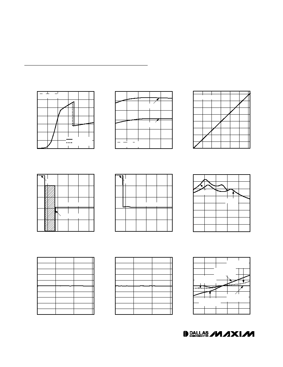
Typical Operating Characteristics
(V
CC
= 5.0V; T
A
= +25°C, unless otherwise noted.)
SUPPLY CURRENT vs. VOLTAGE
DS4301 toc01
VOLTAGE (V)
SUPPLY CURRENT (
µ
A)
5
4
3
2
1
5
10
15
20
30
25
35
0
0
CS = INC = U/D = V
CC
POWER-UP
POWER-DOWN
SUPPLY CURRENT vs. TEMPERATURE
DS4301 toc02
TEMPERATURE (
°C)
SUPPLY CURRENT (
µ
A)
60
35
10
-15
5
10
15
20
25
30
0
-40
85
V
CC
= 3V
V
CC
= 5V
CS = INC = U/D = V
CC
W-L RESISTANCE
vs. POTENTIOMETER SETTING
DS4301 toc03
POTENTIOMETER SETTING (DEC)
W-L RESISTANCE (k
)
30
25
15
20
10
5
25
50
75
100
125
150
175
200
0
0
AT V
CC
= 5V AND 3V
W-L RESISTANCE vs. SUPPLY VOLTAGE
(POWER-UP)
DS4301 toc04
SUPPLY VOLTAGE (V)
W-L RESISTANCE (k
)
5
4
3
2
1
50
100
150
200
250
0
0
>1M
EEPROM RECALL
WIPER = POS 15
W-L RESISTANCE vs. SUPPLY VOLTAGE
(POWER-DOWN)
DS4301 toc05
SUPPLY VOLTAGE (V)
W-L RESISTANCE (k
)
5
4
3
2
1
50
100
150
200
250
0
0
>1M
WIPER = POS 15
WIPER RESISTANCE vs. WIPER VOLTAGE
DS4301 toc06
WIPER VOLTAGE (V)
WIPER RESISTANCE (
)
4
3
1
2
50
100
150
200
300
250
350
400
0
0
5
V
CC
= 3V
V
CC
= 5V
ABSOLUTE LINEARITY vs. WIPER POSITION
DS4301 toc07
WIPER POSITION (DEC)
ABSOLUTE LINEARITY (LSB)
30
20
10
-0.20
-0.15
-0.10
-0.05
0
0.05
0.10
0.15
0.20
0.25
-0.25
0
RELATIVE LINEARITY vs. WIPER POSITION
DS4301 toc08
WIPER POSITION (DEC)
ABSOLUTE LINEARITY (LSB)
30
20
10
-0.20
-0.15
-0.10
-0.05
0
0.05
0.10
0.15
0.20
0.25
-0.25
0
VOLTAGE DIVIDER PERCENT CHANGE
FROM +25
°C vs. TEMPERATURE
DS4301 toc09
TEMPERATURE (
°C)
% CHANGE (FROM +25
°
C)
60
35
10
-15
-0.04
-0.03
-0.02
-0.01
0
0.01
0.02
0.03
0.04
0.05
-0.05
-40
85
WIPER = POS 15
tc = 0.64ppm/
°C
WIPER = POS 7
tc = 2.72ppm/
°C
WIPER = POS 7
tc = 2.72ppm/
°C
WIPER = POS 15
tc = 1.37ppm/
°C
WIPER = POS 23
tc = 0ppm/
°C
DS4301
Nonvolatile, 32-Position Digital Potentiometer
_____________________________________________________________________
5
Typical Operating Characteristics (continued)
(V
CC
= 5.0V; T
A
= +25°C, unless otherwise noted.)
END-TO-END RESISTANCE PERCENT
CHANGE FROM +25
°C vs. TEMPERATURE
DS4301 toc10
TEMPERATURE (
°C)
% CHANGE (FROM +25
°
C)
60
40
20
0
-20
-4
-3
-2
-1
0
1
2
3
4
5
-5
-40
80
-37.18ppm/
°C = tc
-148.38ppm/
°C = tc
TEMPERATURE COEFFICIENT
vs. POTENTIOMETER SETTING
DS4301 toc11
POTENTIOMETER SETTING (DEC)
TEMPERATURE COEFFICIENT (ppm/
°
C)
30
25
15
20
10
5
-8
-6
-4
-2
0
2
4
6
8
10
-10
0
25
°C TO 85°C
+25
°C TO -40°C
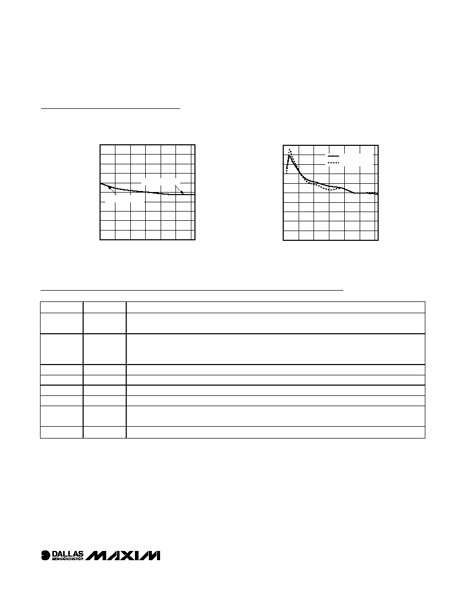
Pin Description
PIN
NAME
FUNCTION
1
INC
Increment/Decrement Wiper Control. When INC transitions from high-to-low, the wiper moves in the
direction established by the state of the U/D pin.
2
U/D
Up/Down Control. Sets the directions of wiper movement. When set to a high state, a high-to-low
transition on the INC pin increments the wiper. When set to a low state, a high-to-low transition on the
INC pin decrements the wiper.
3
H
High-End Terminal of the Potentiometer
4
GND
Ground Terminal
5
W
Wiper Terminal of the Potentiometer
6
L
Low-End Terminal of the Potentiometer
7
CS
Chip Select. When set to a low state, the wiper position can be adjusted using U/D and INC. When in
a high-state, activity on INC and U/D does not affect or change the wiper position.
8
V
CC
Power Supply Terminal