Äîêóìåíòàöèÿ è îïèñàíèÿ www.docs.chipfind.ru
General Description
The DS3930 contains six 256-position nonvolatile (NV)
potentiometers, 64 bytes of NV user EEPROM memory,
and four programmable NV I/O pins. The six poten-
tiometers all share a common low side. The potentiome-
ters are separated into two groups of three 50k
potentiometers in parallel. Each group of three poten-
tiometers shares a common high side and forms an
equivalent resistance of 16.6k
(three 50k poten-
tiometers in parallel).
Applications
RF Transceivers
Voltage References
Power Supply Calibration
Mobile Phones and PDAs
Fiber Optic Transceiver Modules
Portable Electronics
Radio Tuners
Small, Low-Cost Replacement for Mechanical
Potentiometers
Features
Six 256-Position NV Potentiometers
Four General-Purpose NV I/O Pins
64 Bytes of User EEPROM Memory
0 to 5.5V on Any Potentiometer Terminal,
Independent of V
CC
All Six Potentiometers Share a Common Low Side
Potentiometers Separated into Two Groups of
Three Potentiometers, Each Sharing a Common
High Side
2-Wire Serial Interface
Wide Supply Range (2.7V to 5.5V)
Up to Eight DS3930s Can Share the Same
2-Wire Bus
DS3930
Hex Nonvolatile Potentiometer with
I/O and Memory
_____________________________________________ Maxim Integrated Products
1
20
19
18
17
16
15
14
13
1
2
3
4
5
6
7
8
HI
0-2
W
0
W
1
W
2
SDA
A2
A1
A0
TOP VIEW
LO
0-5
HI
3-5
W
3
W
4
I/O
2
I/O
1
I/O
0
SCL
12
11
9
10
W
5
I/O
3
GND
V
CC
TSSOP
DS3930
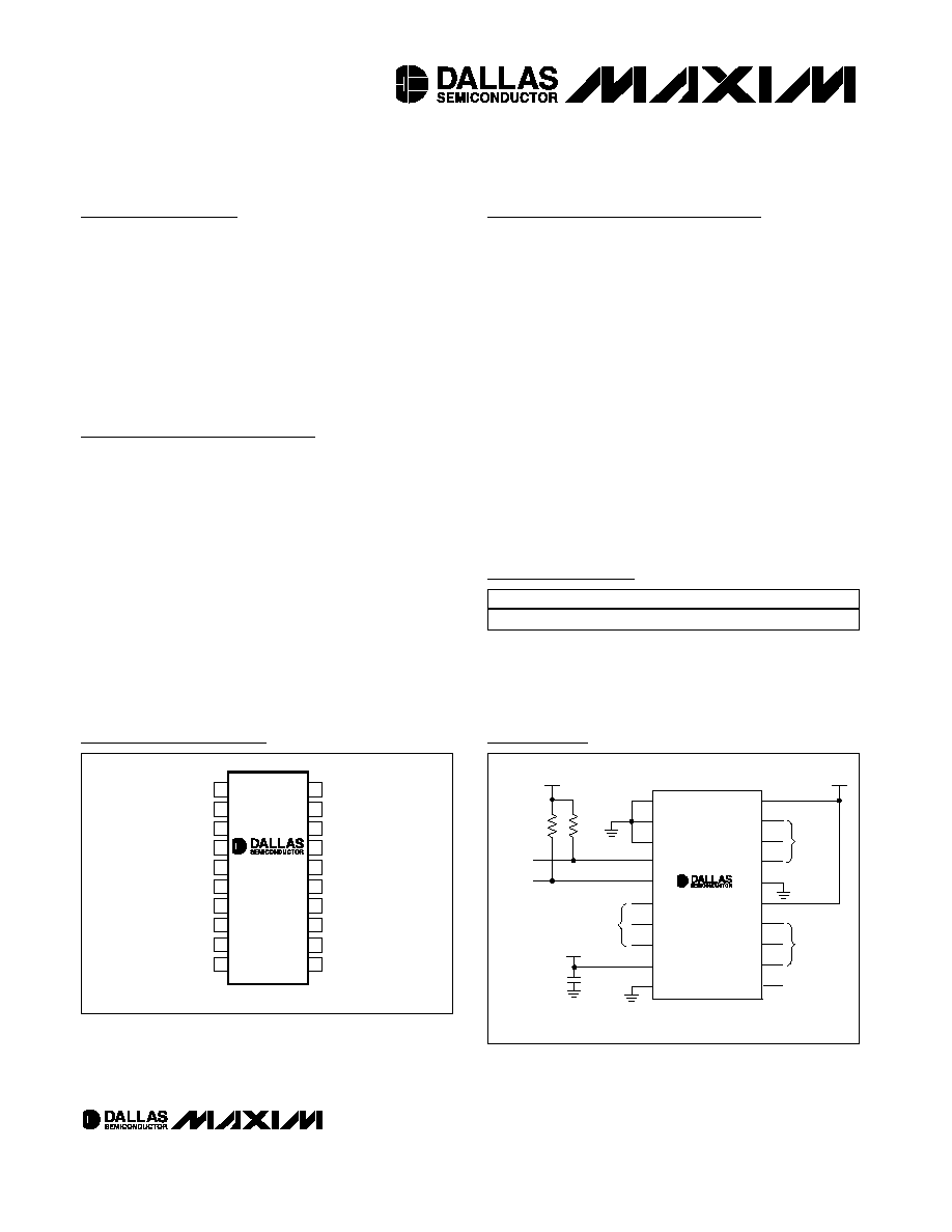
Pin Configuration
A2
SDA
GND
SCL
I/O
3
I/O
2
I/O
1
I/O
0
LO
0-5
A0
A1
HI
0-2
HI
3-5
W
0
W
1
W
2
W
3
W
4
W
5
V
CC
V
CC
V
CC
V
CC
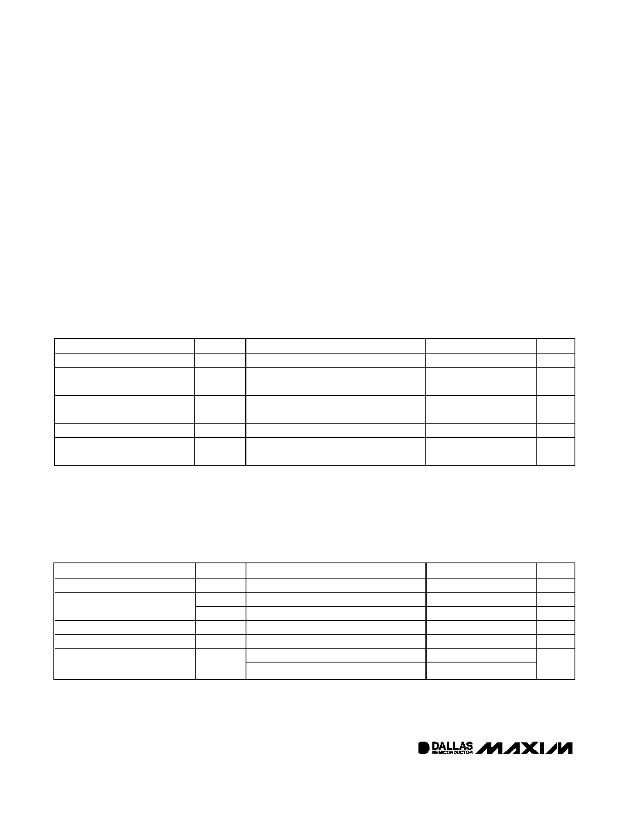
DECOUPLING CAP
0.1
µF
2-WIRE
INTERFACE
4.7k
4.7k
DIGITAL
NONVOLATILE I/O
DIGITAL
NONVOLATILE I/O
WIPER
TERMINALS
WIPER
TERMINALS
DS3930
Typical Operating Circuit
Ordering Information
Rev 0; 4/03
For pricing, delivery, and ordering information, please contact Maxim/Dallas Direct! at
1-888-629-4642, or visit Maxim's website at www.maxim-ic.com.
PART
PIN-PACKAGE
DS3930E
20 TSSOP
DS3930
Hex Nonvolatile Potentiometer with
I/O and Memory
2
______________________________________________________________________
ABSOLUTE MAXIMUM RATINGS
RECOMMENDED DC OPERATING CONDITIONS
(T
A
= -40° to +85°C)
Stresses beyond those listed under "Absolute Maximum Ratings" may cause permanent damage to the device. These are stress ratings only, and functional
operation of the device at these or any other conditions beyond those indicated in the operational sections of the specifications is not implied. Exposure to
absolute maximum rating conditions for extended periods may affect device reliability.
Voltage on V
CC
Relative to Ground ...................... -0.5V to +6.0V
Voltage on I/O
0
, I/O
1
, I/O
2
, I/O
3
, SDA, SCL, A0, A1, and A2
Relative to Ground* .............................. -0.5V to (V
CC
+ 0.5V)
Voltage on LO
0-5
, W
0-5
, HI
0-2
, and HI
3-5
Relative to Ground ............................................-0.5V to +6.0V
Current Through W
0-5
........................................................ ±1mA
Operating Temperature Range .......................... -40°C to +85°C
Programming Temperature Range .........................0°C to +70°C
Storage Temperature Range .............................-55°C to +125°C
Soldering Temperature.................. See IPC/JEDEC J-STD-020A
PARAMETER
SYMBOL
CONDITIONS
MIN
TYP
MAX
UNITS
Supply Voltage
V
CC
(Note 1)
+2.7
+5.5
V
Input Logic 1 (SDA, SCL, A0, A1,
A2, I/O
0
, I/O
1
, I/O
2
, I/O
3
)
V
IH
0.7 x
V
CC
V
CC
+
0.3
V
Input Logic 0 (SDA, SCL, A0, A1,
A2, I/O
0
, I/O
1
, I/O
2
, I/O
3
)
V
IL
-0.3
0.3 x
V
CC
V
Wiper Current
I
W
-1
+1
mA
Potentiometer Terminals
(LO
0-5
, W
0-5
, HI
0-2
, and HI
3-5)
V
CC
= +2.7V to +5.5V
-0.3
+5.5
V
DC ELECTRICAL CHARACTERISTICS
(V
CC
= +2.7V to +5.5V; T
A
= -40°C to +85°C, unless otherwise specified.)
PARAMETER
SYMBOL
CONDITIONS
MIN
TYP
MAX
UNITS
Input Leakage
I
IL
-1
+1
µA
V
OL1
3mA sink current
0
0.4
V
Low-Level Output Voltage (SDA,
I/O
0
, I/O
1
, I/O
2
, I/O
3
)
V
OL2
6mA sink current
0
0.6
V
I/O Capacitance
C
I/O
10
pF
I/O Pullup Resistor Value
R
I/O
3.5
5
7.0
k
3V (Note 2)
160
300
Standby Current
I
STBY
5V (Note 2)
195
350
µA
*This voltage must not exceed 6.0V.
DS3930
Hex Nonvolatile Potentiometer with
I/O and Memory
_____________________________________________________________________
3
AC ELECTRICAL CHARACTERISTICS
(V
CC
= +2.7V to +5.5V; T
A
= -40°C to +85°C, unless otherwise specified.)
PARAMETER
SYMBOL
CONDITIONS
MIN
TYP
MAX
UNITS
Fast mode
0
400
SCL Clock Frequency (Note 3)
f
SCL
Standard mode
0
100
kHz
Fast mode
1.3
Bus Free Time Between STOP
and START Condition (Note 3)
t
BUF
Standard mode
4.7
µs
Fast mode
0.6
Hold Time (Repeated) START
Condition (Notes 3 and 4)
t
HD:STA
Standard mode
4.0
µs
Fast mode
1.3
Low Period of SCL Clock (Note 3)
t
LOW
Standard mode
4.7
µs
Fast mode
0.6
High Period of SCL Clock
(Note 3)
t
HIGH
Standard mode
4.0
µs
ANALOG RESISTOR CHARACTERISTICS
(V
CC
= +2.7V to +5.5V; T
A
= -40°C to +85°C, unless otherwise specified.)
PARAMETER
SYMBOL
CONDITIONS
MIN
TYP
MAX
UNITS
End-to-End Resistance
T
A
= +25°C (three 50k
pots in parallel)
13.2
16.5
19.8
k
Wiper Resistance
R
W
400
1000
Factory Default Wiper Setting
FF
Hex
Factory Default I/O Setting
0F
Hex
POT-to-POT Matching
-1
+1
LSB
Differential Linearity
-0.5
+0.5
LSB
Integral Linearity
-1
+1
LSB
End-to-End Temperature
Coefficient
3 potentiometers in parallel
-250
0
+250
ppm/°C
Ratiometric Temperature
Coefficient
2
ppm/°C
DS3930
Hex Nonvolatile Potentiometer with
I/O and Memory
4
______________________________________________________________________
Note 1:
All voltages are referenced to ground.
Note 2:
I
STBY
specified for V
CC
equal 3.0V and 5.0V, SDA = SCL = V
CC
, and I/O
0
= I/O
1
= I/O
2
= I/O
3
= A0 = A1 = A2 = GND.
Note 3:
A fast-mode device can be used in a standard-mode system, but the requirement t
SU:DAT
> 250ns must then be met.
This is automatically the case if the device does not stretch the LOW period of the SCL signal. If such a device does
stretch the LOW period of the SCL signal, it must output the next data bit to the SDA line t
RMAX
+ t
SU:DAT
= 1000ns
+250ns = 1250ns before the SCL line is released.
Note 4:
After this period, the first clock pulse is generated.
Note 5:
The maximum t
HD:DAT
has only to be met if the device does not stretch the LOW period (t
LOW
) of the SCL signal.
Note 6:
A device must internally provide a hold time of at least 300ns for the SDA signal (referred to the V
IH MIN
of the SCL sig-
nal) in order to bridge the undefined region of the falling edge of SCL.
Note 7:
C
B
--total capacitance of one bus line in picofarads, timing referenced to 0.9V
CC
and 0.1V
CC.
Note 8:
EEPROM write begins after a STOP condition occurs.
AC ELECTRICAL CHARACTERISTICS (continued)
(V
CC
= +2.7V to +5.5V; T
A
= -40°C to +85°C, unless otherwise specified.)
PARAMETER
SYMBOL
CONDITIONS
MIN
TYP
MAX
UNITS
Fast mode
0
0.9
Data Hold Time (Notes 3, 5, 7)
t
HD:DAT
Standard mode
0
0.9
µs
Fast mode
100
Data Setup Time (Note 3)
t
SU:DAT
Standard mode
250
ns
Fast mode
0.6
Start Setup Time (Note 3)
t
SU:STA
Standard mode
4.7
µs
Fast mode
20 + 0.1C
B
300
Rise Time of Both SDA and SCL
Signals (Note 7)
t
R
Standard mode
20 + 0.1C
B
1000
ns
Fast mode
20 + 0.1C
B
300
Fall Time of Both SDA and SCL
Signals (Note 7)
t
F
Standard mode
20 + 0.1C
B
300
ns
Fast mode
0.6
Setup Time for STOP Condition
t
SU:STO
Standard mode
4.0
µs
Capacitive Load for Each Bus
C
B
(Note 7)
400
pF
EEPROM Write Time
t
W
(Note 8)
5
20
ms
EEPROM CHARACTERISTICS
(V
CC
= +2.7V to +5.5V; T
A
= -40°C to +85°C, unless otherwise specified.)
PARAMETER
SYMBOL
CONDITIONS
MIN
TYP
MAX
UNITS
Writes
+70°C
50,000
DS3930
Hex Nonvolatile Potentiometer with
I/O and Memory
_____________________________________________________________________
5
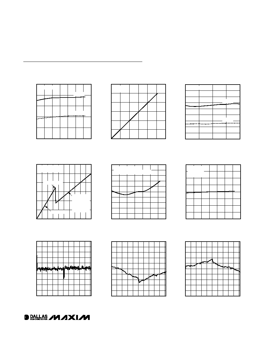
VOLTAGE DIVIDER % CHANGE
FROM +25
°C vs. TEMPERATURE
DS3930 toc06
TEMPERATURE (
°C)
RESISTANCE % CHANGE (FROM +25
°
C)
80
60
-20
0
20
40
-0.15
-0.10
-0.05
0
0.05
0.10
0.15
0.20
-0.20
-40
100
HI = V
CC
LO
0-5
= GND
POSITION 127
END-TO-END RESISTANCE % CHANGE
FROM +25
°C vs. TEMPERATURE
DS3930 toc05
TEMPERATURE (
°C)
RESISTANCE % CHANGE (FROM +25
°
C)
80
60
20
40
0
-20
-0.80
-0.60
-0.40
-0.20
0
0.20
0.40
0.60
0.80
1.00
-1.00
-40
100
3 POTS IN PARALLEL
MEASURED FROM HI
0-2
TO LO
0-5
WIPER VOLTAGE
vs. POWER-UP VOLTAGE
DS3930 toc04
POWER-UP VOLTAGE (V)
WIPER VOLTAGE (V)
4.5
4.0
3.5
3.0
2.5
2.0
1.5
1.0
0.5
0.5
1.0
1.5
2.0
2.5
3.0
0
0
5.0
HI = 5V, LO = GND
POSITION 127
EEPROM RECALL
FOLLOWS V
CC
CHANGES TO
PROGRAMMED
VALUE ONCE
EEPROM IS
RECALLED
ACTIVE SUPPLY CURRENT
vs. SCL FREQUENCY
DS3930 toc03
SCL FREQUENCY (kHz)
SUPPLY CURRENT (
µ
A)
300
200
100
260
320
380
440
500
560
620
680
740
200
0
400
V
CC
= 5V
V
CC
= 3V
SDA = V
CC
WIPER VOLTAGE vs. WIPER SETTING
DS3930 toc02
SETTING (DEC)
VOLTAGE (V)
250
200
150
100
50
1
2
3
4
5
6
0
0
300
HI = 5V
LO = GND
SUPPLY CURRENT vs. TEMPERATURE
DS3930 toc01
TEMPERATURE (
°C)
SUPPLY CURRENT (
µ
A)
80
60
40
20
0
-20
140
160
180
200
220
120
-40
100
V
CC
= 5V
V
CC
= 3V
SDA = SCL = 5V
Typical Operating Characteristics
(V
CC
= 5.0V; T
A
= +25°C, unless otherwise specified.)
ALL POTS DNL (LSB)
DS3930 toc08
POSITION (DEC)
DNL (LSB)
225
200
150 175
50 75 100 125
25
-0.08
-0.06
-0.04
-0.02
0
0.02
0.04
0.06
0.08
0.10
-0.10
0
250
POTS 1, 3, 5 INL (LSB)
DS3930 toc09
POSITION (DEC)
INL (LSB)
225
200
150 175
50 75 100 125
25
-0.4
-0.3
-0.2
-0.1
0
0.1
0.2
0.3
0.4
0.5
-0.5
0
250
POTS 0, 2, 4, INL (LSB)
DS3930 toc07
POSITION (DEC)
INL (LSB)
225
200
150 175
50 75 100 125
25
-0.4
-0.3
-0.2
-0.1
0
0.1
0.2
0.3
0.4
0.5
-0.5
0
250