1 of 24
102199
FEATURES
§
Four high-impedance inputs to measure
analog voltages over the 1-Wire bus
§
User programmable input range (2.56V,
5.12V), resolution (1 to 16 bits) and alarm
thresholds
§
5V, single supply operation
§
Very low power: 2.5 mW active, 25
µ
W idle
§
Built-in multidrop controller allows multiple
DS2450's to be identified and operated on a
common 1-Wire bus
§
Responds to Conditional Search if the analog
voltage crosses the alarm thresholds
§
Channels not used as analog input can serve
as open drain digital outputs for closed-loop
control
§
Directly connects to a single port pin of a
microprocessor and communicates at up to
16.3k bits per second
§
Overdrive mode boosts communication speed
to 142k bits per second
§
On-chip 16-bit CRC-generator for
safeguarding data transfers
§
Unique, factory-lasered and tested 64-bit
registration number (8-bit family code + 48-
bit serial number 8-bit CRC tester) assures
absolute traceability because no two parts are
alike
§
8-bit family code specifies device
communication requirements to bus master
§
Operating temperature range from -40
°
C to
+85
°
C
§
Compact, low cost 8-pin SOIC surface mount
package
PIN ASSIGNMENT
PIN DESCRIPTION
V
CC
4.5 to 5.5 Volts
NC
Do Not Connect
DATA
1-Wire Bus
GND
Ground
AIN-A
Analog Input A
AIN-B
Analog Input B
AIN-C
Analog Input C
AIN-D
Analog Input D
ORDERING INFORMATION
DS2450S
8-pin SOIC
DESCRIPTION
The DS2450 1-Wire Quad A/D Converter is based on a successive-approximation analog to digital
converter with a four to one analog multiplexer. Each input channel has its own register set to store the
input voltage range, resolution, and alarm threshold values as well as flags to enable participation of the
device in the conditional search if the input voltage leaves the specified range. Two alarm flags for each
channel indicate if the voltage measured was too high or too low without requiring the bus master to do
DS2450
1-Wire
TM
Quad A/D Converter
www.dalsemi.com
V
CC
NC
DATA
GND
AIN-A
AIN-B
AIN-C
AIN-D
2
3
4
8
7
6
5
1
8-PIN SOIC (208 MIL)
DS2450
2 of 24
102199
the comparison. Each A/D conversion is initiated by the bus master. A channel not used as analog input
can serve as a digital open-drain output. After disabling the input the bus master can directly switch on or
off the open-drain transistor at the selected channel. All device settings are stored in SRAM and kept
non-volatile while the device gets power either through the 1-Wire bus or through its V
CC
pin. After
powering up a power-on reset flag signals the bus master the need to restore the device settings before the
regular operation can resume. All device registers and conversion read-out registers are organized as
three 8-byte memory pages similar to the Status Memory of a DS2505/6 device. An on-chip CRC16
generator protects the communication against transmission errors when reading through the end of a
memory page as well as when writing individual bytes.
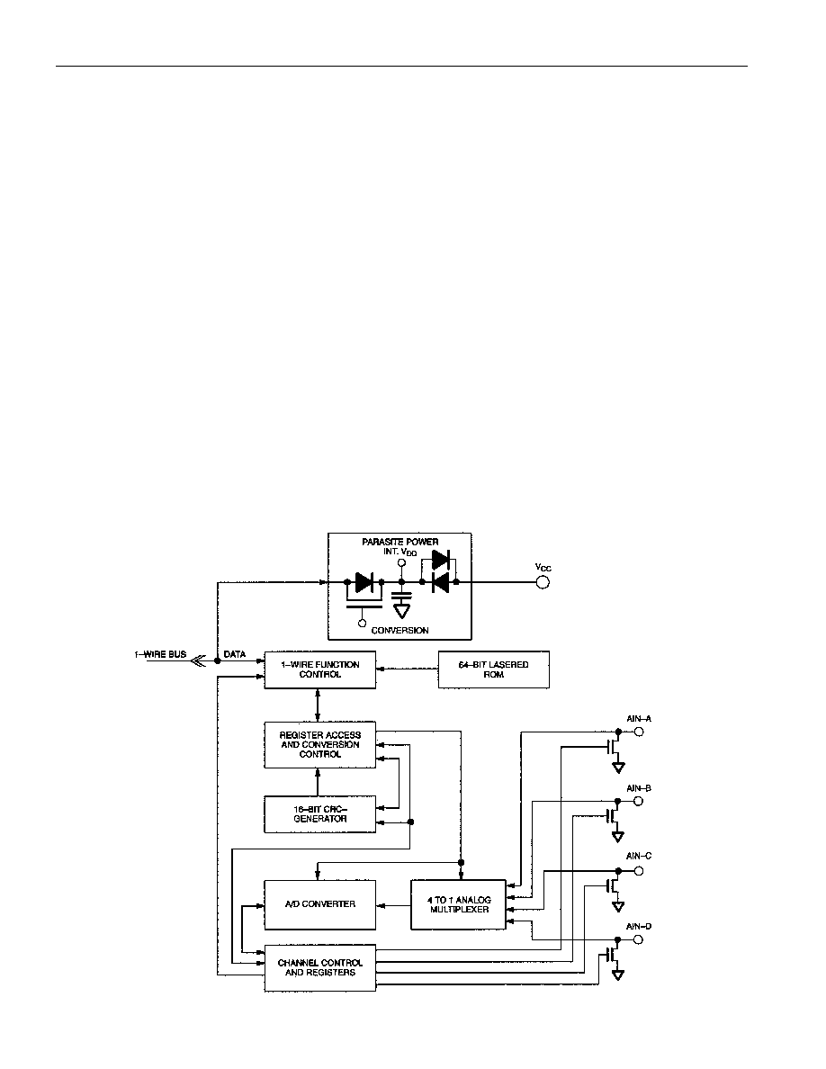
OVERVIEW
The block diagram in Figure 1 shows the major function blocks of the device. The DS2450 contains a
factory-lasered registration number that includes a unique 48-bit serial number, an 8-bit CRC, and an 8-
bit family code (20H). The 64-bit ROM portion of the DS2450 not only creates an absolutely unique
electronic identification for the device itself but also is a means to locate and address the device in order
to exercise its control functions.
The device gets its power either from the 1-Wire bus or through its V
CC
pin. Without a V
CC
supply the
device stores energy on an internal capacitor during periods where the signal line is high and continues to
operate off of this "parasite" power source during the low times of the 1-Wire line until it returns to high
to replenish the parasite (capacitor) supply. This, however, provides sufficient energy only for
communication. To perform an A/D conversion a strong pullup of the 1-Wire bus to 5V or a V
CC
supply
is required.
DS2450 BLOCK DIAGRAM Figure 1
DS2450
3 of 24
102199
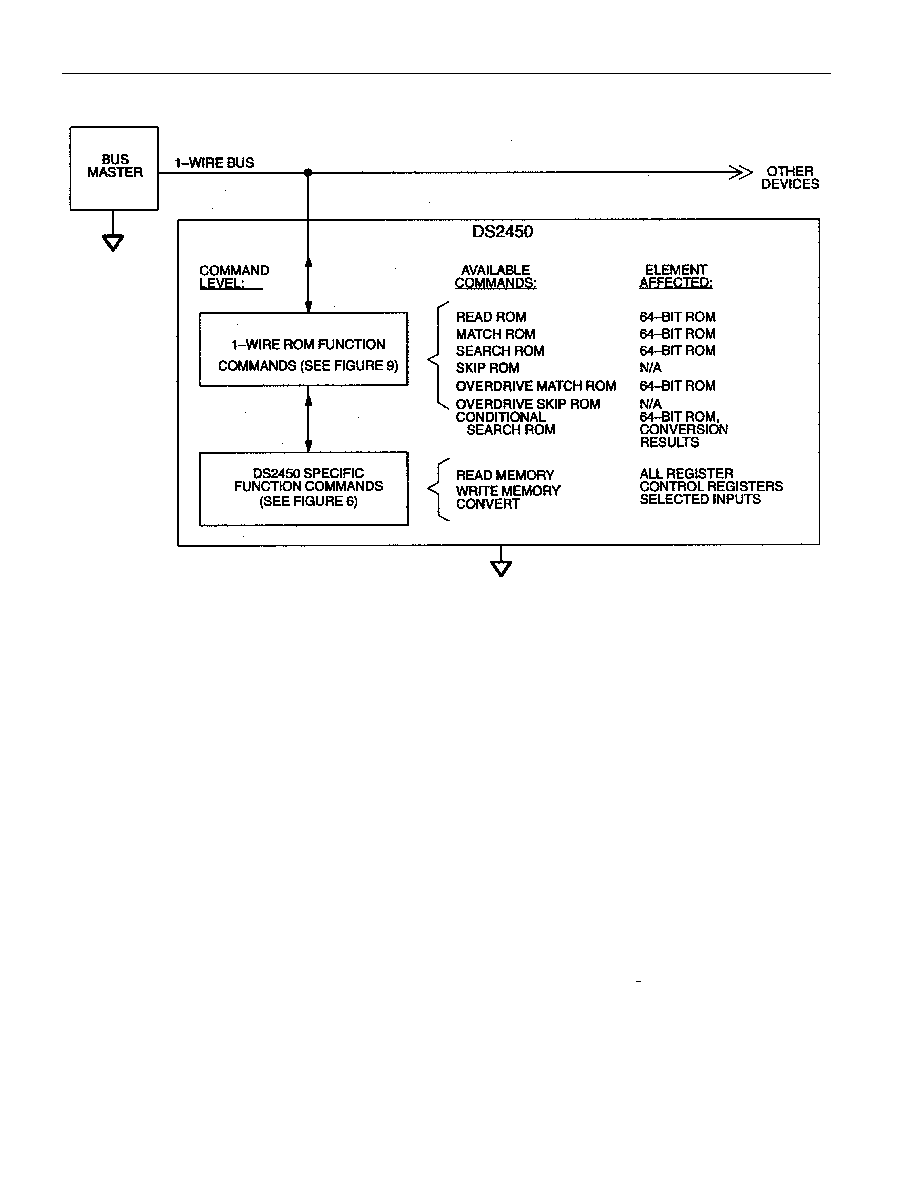
HIERARCHICAL STRUCTURE FOR 1-WIRE PROTOCOL Figure 2
The DS2450 uses the standard Dallas Semiconductor 1-Wire protocol for data transfers. Communication
to and from the DS2450 requires a single bi-directional line that is typically a port pin of a
microcontroller. The hierarchical structure of the 1-Wire protocol is shown in Figure 2. The 1-Wire bus
master must first provide one of the seven ROM Function Commands, 1) Read ROM, 2) Match ROM, 3)
Search ROM, 4) Conditional Search ROM, 5) Skip ROM, 6) Overdrive-Skip ROM or 7) Overdrive-
Match ROM. Upon completion of an overdrive ROM command byte executed at standard speed, the
device will enter Overdrive mode where all subsequent communication occurs at a higher speed. The
protocol required for these ROM function commands is described in Figure 9. After a ROM function
command is successfully executed, the memory and control functions become accessible and the master
may provide any one of the available commands. The protocol for these commands is described in Figure
6. All data is read and written least significant bit first.
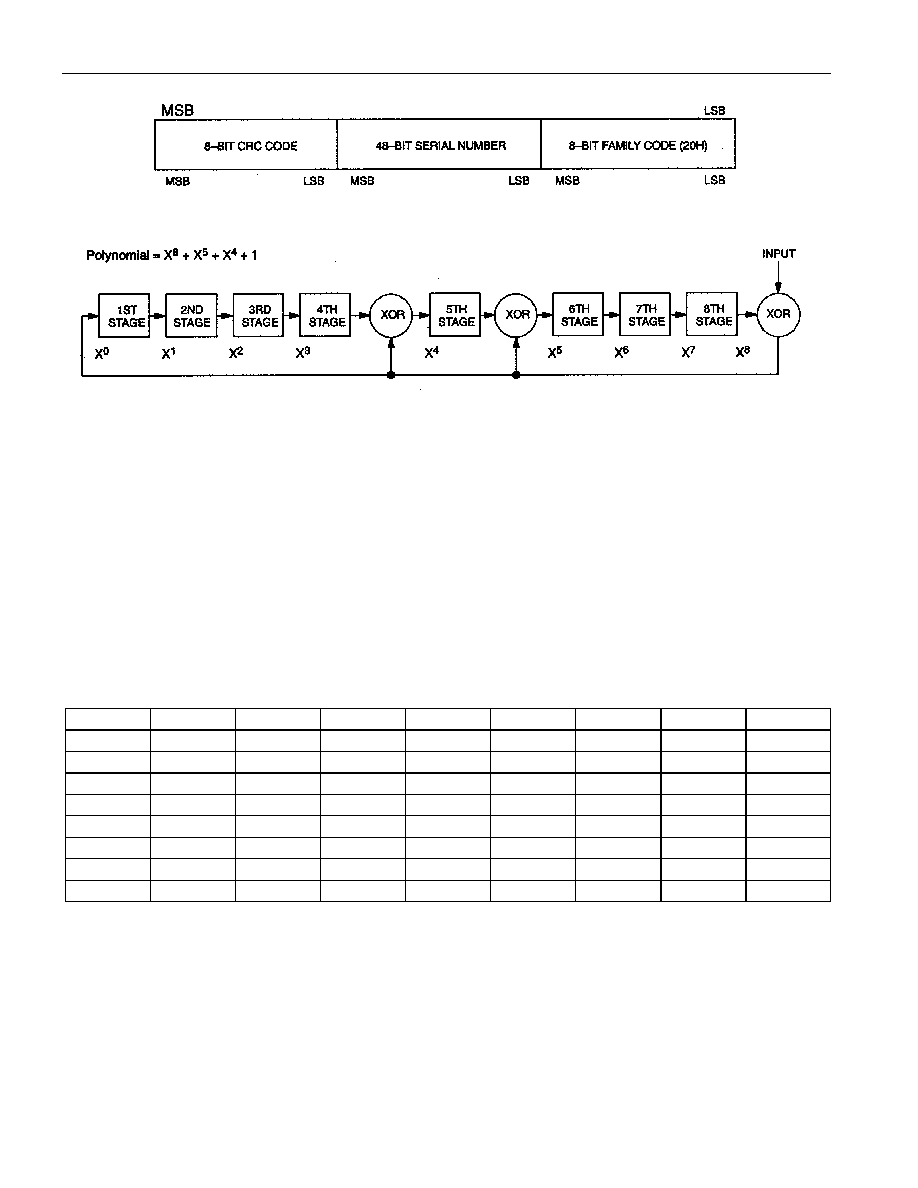
64-BIT LASERED ROM
Each DS2450 contains a unique ROM code that is 64 bits long. The first eight bits are a 1-Wire family
code. The next 48 bits are a unique serial number. The last eight bits are a CRC of the first 56 bits. (See
Figure 3.) The 1-Wire CRC is generated using a polynomial generator consisting of a shift register and
XOR gates as shown in Figure 4. The polynomial is X
8
+ X
5
+ X
4
+ 1. Additional information about the
Dallas 1-Wire Cyclic Redundancy Check is available in the Book of DS19xx iButton
TM
Standards. The
shift register acting as the CRC accumulator is initialized to zero. Then starting with the least significant
bit of the family code, one bit at a time is shifted in. After the 8
th
bit of the family code has been entered,
then the serial number is entered. After the 48
th
bit of the serial number has been entered, the shift
register contains the CRC value. Shifting in the eight bits of CRC should return the shift register to all
zeros.
DS2450
4 of 24
102199
64-BIT LASERED ROM Figure 3
1-WIRE CRC-GENERATOR Figure 4
DEVICE REGISTERS
All registers of the DS2450 are mapped into a linear memory range of 24 adjacent bytes organized as
three 8-byte pages. The first page, called conversion read-out, contains the memory area where the chip-
internal logic places the results of a conversion for the bus master to read. Starting with channel A at the
lowest address, each channel has an area of 16 bits assigned for the conversion result, as shown in Figure
5a. The power-on default for the conversion read-out registers is all zeros. Regardless of the resolution
requested, the most significant bit of the conversion is always at the same bit position. If less than 16-bit
resolution is requested, the least significant bits of the conversion result will be filled with zeros in order
to always generate a 16-bit result. For applications that require less than four analog inputs, one should
start using input D for the first channel, input C for the second one, etc. The advantage is that when
reading the conversion results one reaches the end of the page and with it the CRC16 sooner and
minimizes the traffic on the 1-Wire bus. For more details on reading please refer to the Read Memory
command description.
MEMORY MAP PAGE 0, CONVERSION READ-OUT Figure 5a
Address
bit 7
bit 6
bit 5
bit 4
bit 3
bit 2
bit 1
bit 0
00
A
A
A
A
A
A
A
LSBIT A
01
MSBIT A
A
A
A
A
A
A
A
02
B
B
B
B
B
B
B
LSBIT B
03
MSBIT B
B
B
B
B
B
B
B
04
C
C
C
C
C
C
C
LSBIT C
05
MSBIT C
C
C
C
C
C
C
C
06
D
D
D
D
D
D
D
LSBIT D
07
MSBIT D
D
D
D
D
D
D
D
The control and status information for all channels is located in memory page 1 (Figure 5b). As for the
conversion read-out, each channel has assigned 16 bits. The four least significant bits, called RC3 to
RC0, are an unsigned binary number that represents the number of bits to be converted. A code of 1111
(15 decimal) will generate a 15-bit result. For a full 16-bit conversion the code number needs to be 0000.
The next two bits beyond RC3 will always read 0. They have no function and cannot be changed to 1s.

DS2450
5 of 24
102199
The next bits, OC (output control) and OE (enable output) control the alternate use of a channel as output.
For normal operation as analog input the OE bit of a channel needs to be 0, rendering the OC bit to a
don't care. With OE set to 1, a 0 for OC will make the channel's output transistor conducting, a 1 for OC
will switch the transistor off. With a pullup resistor to a positive voltage, for example, the OC bit will
directly translate into the voltage equivalent of its logic state. Enabling the output does not disable the
analog input. Conversions remain possible, but will result in values close to 0 if the transistor is
conducting.
The IR bit in the second byte of a channel's control and status memory selects the input voltage range.
With IR set to 0, the highest possible conversion result is reached at 2.55V. Setting IR to 1 requires an
input voltage of 5.10V for the same result. The next bit beyond IR has no function. It will always read 0
and cannot be changed to 1.
The next two bits, AEL alarm enable low and AEH alarm enable high, control whether the device will
respond to the Conditional Search command (see ROM Functions) if a conversion results in a value
higher (AEH) than or lower (AEL) than the channel's alarm threshold voltage as specified in the alarm
settings. The alarm flags AFL (low) and AFH (high) tell the bus master whether the channel's input
voltage was beyond the low or high threshold at the latest conversion. These flags are cleared
automatically if a new conversion reveals a non-alarming value. They can alternatively be written to 0 by
the bus master without a conversion.
The next bit of a channel's control and status memory always reads 0 and cannot be changed to 1. The
POR bit (power on reset) is automatically set to 1 as the device performs a power-on reset cycle. As long
as this bit is set the device will always respond to the Conditional Search command in order to notify the
bus master that the control and threshold data is no longer valid. After powering-up the POR bit needs to
be written to 0 by the bus master. This may be done together with restoring the control and threshold
data. It is possible for the bus master to write the POR bit to a 1. This will make the device participate in
the conditional search but will not
generate a reset cycle. Since the POR bit is related to the device and
not channel-specific the value written with the most recent setting of an input range or alarm enable
applies. The power-on default setting for the control/status data is 08h for the first and 8Ch for the
second byte of each channel.
MEMORY MAP PAGE 1, CONTROL/STATUS DATA Figure 5b
Address
bit 7
bit 6
bit 5
bit 4
bit 3
bit 2
bit 1
bit 0
08
OE-A
OC-A
0
0
RC3-A
RC2-A
RC1-A
RC0-A
09
POR
0
AFH-A
AFL-A
AEH-A
AEL-A
0
IR-A
0A
OE-B
OC-B
0
0
RC3-B
RC2-B
RC1-B
RC0-B
0B
POR
0
AFH-B
AFL-B
AEH-B
AEL-B
0
IR-B
0C
OE-C
OC-C
0
0
RC3-C
RC2-C
RC1-C
RC0-C
0D
POR
0
AFH-C
AFL-C
AEH-C
AEL-C
0
IR-C
0E
OE-D
OC-D
0
0
RC3-D
RC2-D
RC1-D
RC0-D
0F
POR
0
AFH-D
AFL-D
AEH-D
AEL-D
0
IR-D