
1 of 14
082099
SPECIAL FEATURES
§
1,152-bit secure read/write, nonvolatile
memory
§
Secure memory cannot be deciphered
without matching 64-bit password
§
Memory is partitioned into 3 blocks of 384
bits each
§
64-bit password and ID fields for each
memory block
§
512-bit scratchpad ensures data transfer
integrity
§
Operating temperature range: -40°C to
+70°C
§
Over 10 years of data retention
COMMON iButton FEATURES
§
Unique, factory-lasered and tested 64-bit
registration number (8-bit family code + 48-
bit serial number + 8-bit CRC tester) assures
absolute traceability because no two parts are
alike
§
Multidrop controller for MicroLAN
§
Digital identification and information by
momentary contact
§
Chip-based data carrier compactly stores
information
§
Data can be accessed while affixed to object
§
Economically communicates to bus master
with a single digital signal at 16.3k bits per
second
§
Standard 16 mm diameter and 1-Wire
protocol ensure compatibility with iButton
family
§
Button shape is self-aligning with cup-
shaped probes
§
Durable stainless steel case engraved with
registration number withstands harsh
environments
§
Easily affixed with self-stick adhesive
backing, latched by its flange, or locked with
a ring pressed onto its rim
§
Presence detector acknowledges when reader
first applies voltage
§
Meets UL#913 (4th Edit.); Intrinsically Safe
Apparatus, Approved under Entity Concept
for use in Class I, Division 1, Group A, B, C
and D Locations
F5 MICROCAN
TM
All dimensions shown in millimeters
ORDERING INFORMATION
DS1991L-F5
F5 MicroCan
EXAMPLES OF ACCESSORIES
DS9096P
Self-Stick Adhesive Pad
DS9101
Multi-Purpose Clip
DS9093RA
Mounting Lock Ring
DS9093F
Snap-In Fob
DS9092
iButton Probe
DS1991
MultiKey iButton
TM
www.dalsemi.com
DATA
GROUND
0.36
0.51
5.89
c
1993
YYWW REGISTERED RR
21
02
000000FBC52B
16.25
17.35

DS1991
2 of 14
iButton DESCRIPTION
The DS1991 MultiKey iButton is a rugged read/write data carrier that acts as three separate electronic
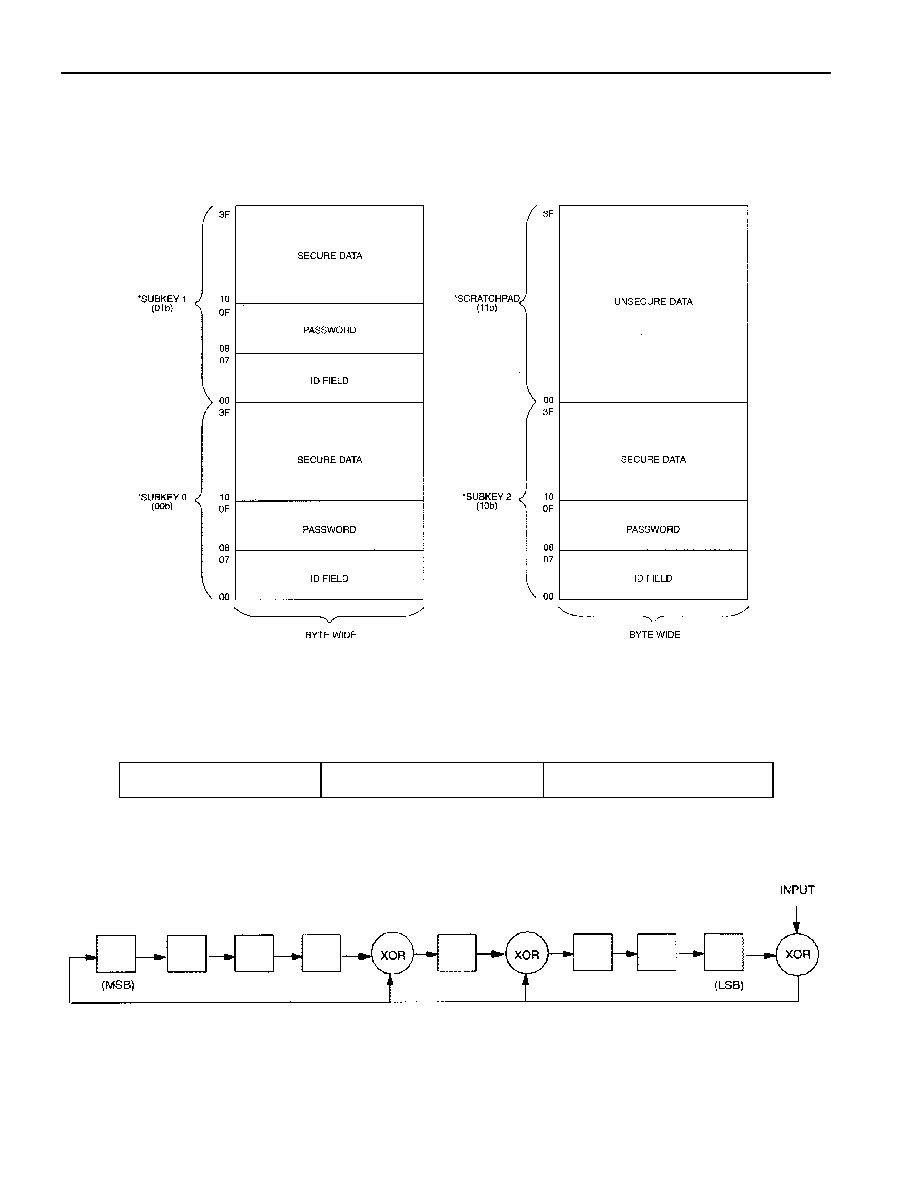
keys, offering 1,152 bits of secure, nonvolatile memory. Each key is 384 bits long with distinct 64-bit
password and public ID fields (Figure 1). The password field must be matched in order to access the
secure memory. Data is transferred serially via the 1-Wire protocol, which requires only a single data lead
and a ground return. The 512-bit scratchpad serves to ensure integrity of data transfers to secure memory.
Data should first be written to the scratchpad where it can be read back. After the data has been verified, a
copy scratchpad command will transfer the data to the secure memory. This process ensures data integrity
when modifying the memory. A 48-bit serial number is factory lasered into each DS1991 to provide a
guaranteed unique identity which allows for absolute traceability. The family code for the DS1991 is 02h.
The durable MicroCan package is highly resistant to environmental hazards such as dirt, moisture and
shock. Its compact button-shaped profile is self-aligning with mating receptacles, allowing the DS1991 to
be easily used by human operators. Accessories permit the DS1991 to be mounted on plastic key fobs,
photo-ID badges, printed-circuit boards or any smooth surface of an object. Applications include secure
access control, debit tokens, work-in-progress tracking, electronic travelers and proprietary data.
OPERATION
The DS1991 is accessed via a single data line using the 1-Wire protocol. The bus master must first
provide one of the four ROM Function Commands, 1) Read ROM, 2) Match ROM, 3) Search ROM, 4)
Skip ROM. These commands operate on the 64-bit lasered ROM portion of each device and can singulate
a specific device if many are present on the 1-Wire line as well as indicate to the bus master how many
and what types of devices are present. The protocol required for these ROM Function Commands is
described in Figure 9. After a ROM Function Command is successfully executed, the memory functions
that operate on the secure memory and the scratchpad become accessible and the bus master may issue
any one of the six Memory Function Commands specific to the DS1991. The protocol for these Memory
Function Commands is described in Figure 5. All data is read and written least significant bit first.
64-BIT LASERED ROM
Each DS1991 contains a unique ROM code that is 64 bits long. The first eight bits are a 1-Wire family
code. The next 48 bits are a unique serial number. The last eight bits are a CRC of the first 56 bits.
(Figure 2.) The 1-Wire CRC is generated using a polynomial generator consisting of a shift register and
XOR gates as shown in Figure 3. The polynomial is X
8
+ X
5
+ X
4
+ 1. Additional information about the
Dallas 1-Wire Cyclic Redundancy Check is available in the Book of DS19xx iButton Standards. The shift
register bits are initialized to zero. Then starting with the least significant bit of the family code, one bit at
a time is shifted in. After the 8th bit of the family code has been entered, then the serial number is
entered. After the 48th bit of the serial number has been entered, the shift register contains the CRC
value. Shifting in the eight bits of CRC should return the shift register to all zeros.
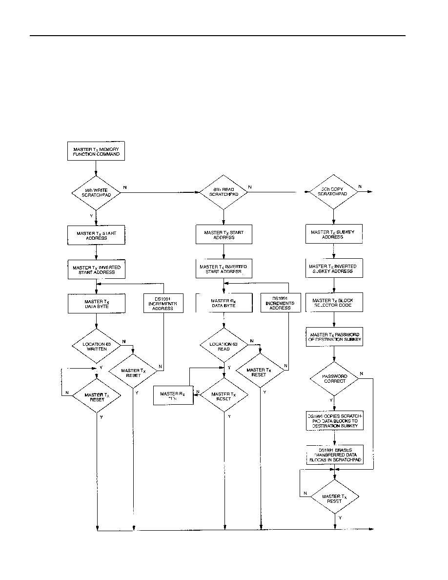
MEMORY FUNCTION COMMANDS
The DS1991 has six device-specific commands. Three scratchpad commands: Write Scratchpad, Read
Scratchpad and Copy Scratchpad and three subkey commands: Write Password, Write Subkey and Read
Subkey. After the device is selected, the memory function command is written to the DS1991. The
command is comprised of three fields, each one byte long. The first byte is the function code field. This
field defines the six commands that can be executed. The second byte is the address field. The first six
bits of this field define the starting address of the command. The last two bits of this field are the subkey
address code. The third byte of the command is a complement of the second byte (Figure 4).
DS1991
3 of 14
For the first use, since the passwords actually stored in the device are unknown, the DS1991 needs to be
initialized. This is done by directly writing (i. e., not through the scratchpad) the new identifier and
password for the selected subkey using the Write Password command. As soon as the new identifier and
password are stored in the device, further updates should be done through the scratchpad.
MEMORY MAP Figure 1
* Each subkey or the scratchpad has its own unique address.
64-BIT LASERED ROM Figure 2
8-Bit CRC Code
48-Bit Serial Number
8-Bit Family Code (02H)
MSB
LSB MSB
LSB MSB
LSB
1-WIRE CRC GENERATOR Figure 3

DS1991
4 of 14
DS1991 COMMAND STRUCTURE Figure 4
2
nd
byte
3
rd
byte
Command
1
st
byte
B7 B6
B5 B4 B3 B2 B1 B0
write
scratchpad
96H
read
scratchpad
69H
1 1
any value
00H to 3FH
copy
scratchpad
3CH
0 0 0 0 0 0
read
SubKey
66H
write
SubKey
99H
any value
10H to 3FH
write
password
5AH
Sub-Key
Nr.:
0
0
or
0
1
or
1
0
0 0 0 0 0 0
ones complement
of 2
nd
byte
SCRATCHPAD COMMANDS
The 64-byte read/write scratchpad of the DS1991 is not password-protected. Its normal use is to build up
a data structure to be verified and then copied to a secure subkey.
Write Scratchpad [96H]
The Write Scratchpad command is used to enter data into the scratchpad. The starting address for the
write sequence is specified in the command. Data can be continuously written until the end of the
scratchpad is reached or until the DS1991 is reset. The command sequence is shown in Figure 5, first
page, left column.
Read Scratchpad [69H]
The Read Scratchpad command is used to retrieve data from the scratchpad. The starting address is
specified in the command word. Data can be continuously read until the end of the scratchpad is reached
or until the DS1991 is reset. The command sequence is shown in Figure 5, first page, center column.
Copy Scratchpad [3CH]
The Copy Scratchpad command is used to transfer specified data blocks from the scratchpad to a selected
subkey. This command should be used when data verification is required before storage in a secure
subkey. Data can be transferred in single 8-byte blocks or in one large 64-byte block. There are nine valid
block selector codes that are used to specify which block is to be transferred (Figure 6). As a further
precaution against accidental erasure of secure data, the 8-byte password of the destination subkey must
be entered. If the password does not match, the operation is terminated. After the block of data is
transferred to the secure subkey, the original data in the corresponding block of the scratchpad is erased.
The command sequence is shown in Figure 5, first page, right column.
SUBKEY COMMANDS
Each of the subkeys within the DS1991 is accessed individually. Transactions to read and write data to a
secured subkey start at the address defined in the command and proceed until the device is reset or the
end of the subkey is reached.
DS1991
5 of 14
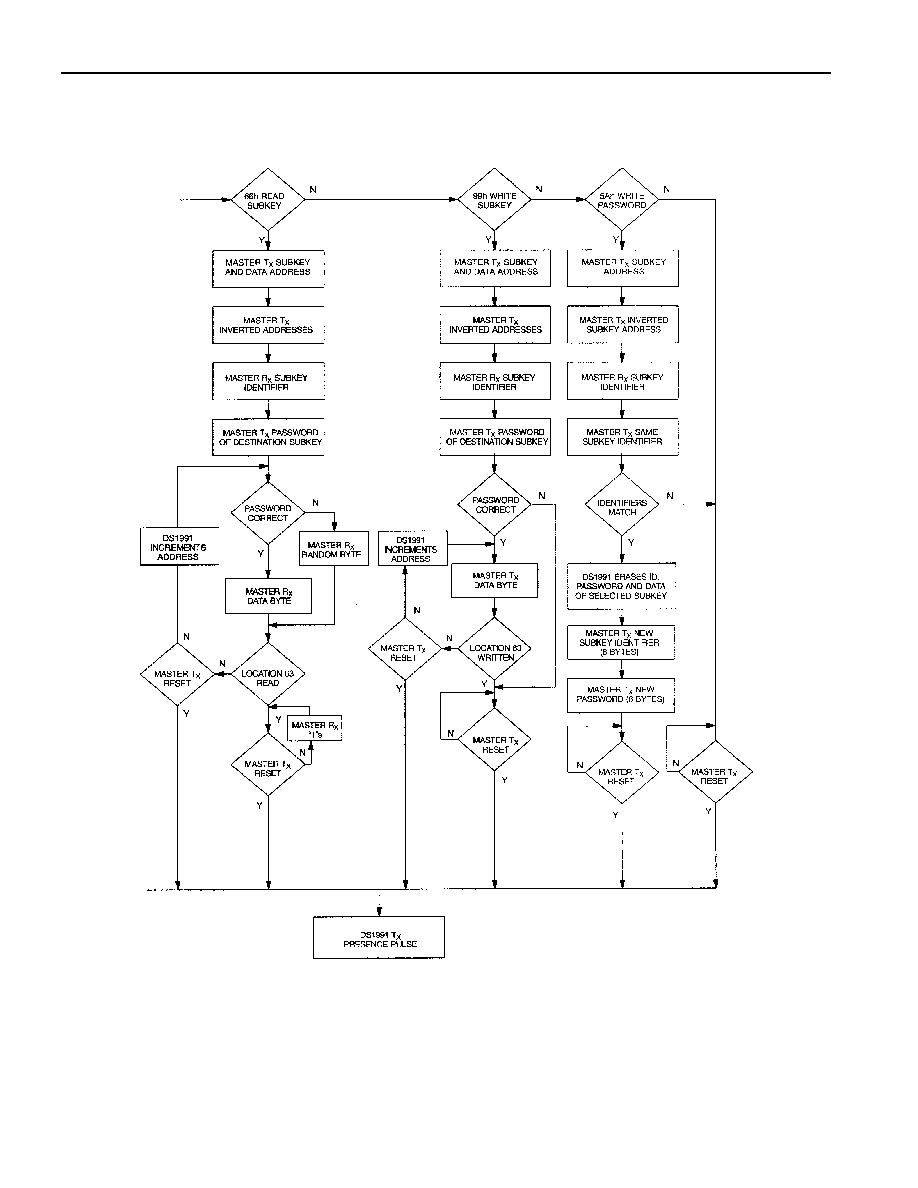
Write Password [5AH]
The Write Password command is used to enter the ID and password of the selected subkey. This
command will erase all of the data stored in the secure area as well as overwriting the ID and password
fields with the new data. The DS1991 has a built-in check to ensure that the proper subkey was selected.
The sequence begins by reading the ID field of the selected subkey; the ID of the subkey to be changed is
then written into the part. If the IDs do not match, the sequence is terminated. Otherwise, the subkey
contents are erased and 64 bits of new ID data are written followed by a new 64-bit password. The
command sequence is shown in Figure 5, 2nd page, right column.
MEMORY FUNCTIONS FLOW CHART Figure 5
DS1991
6 of 14
MEMORY FUNCTIONS FLOW CHART (cont'd) Figure 5
DS1991
7 of 14
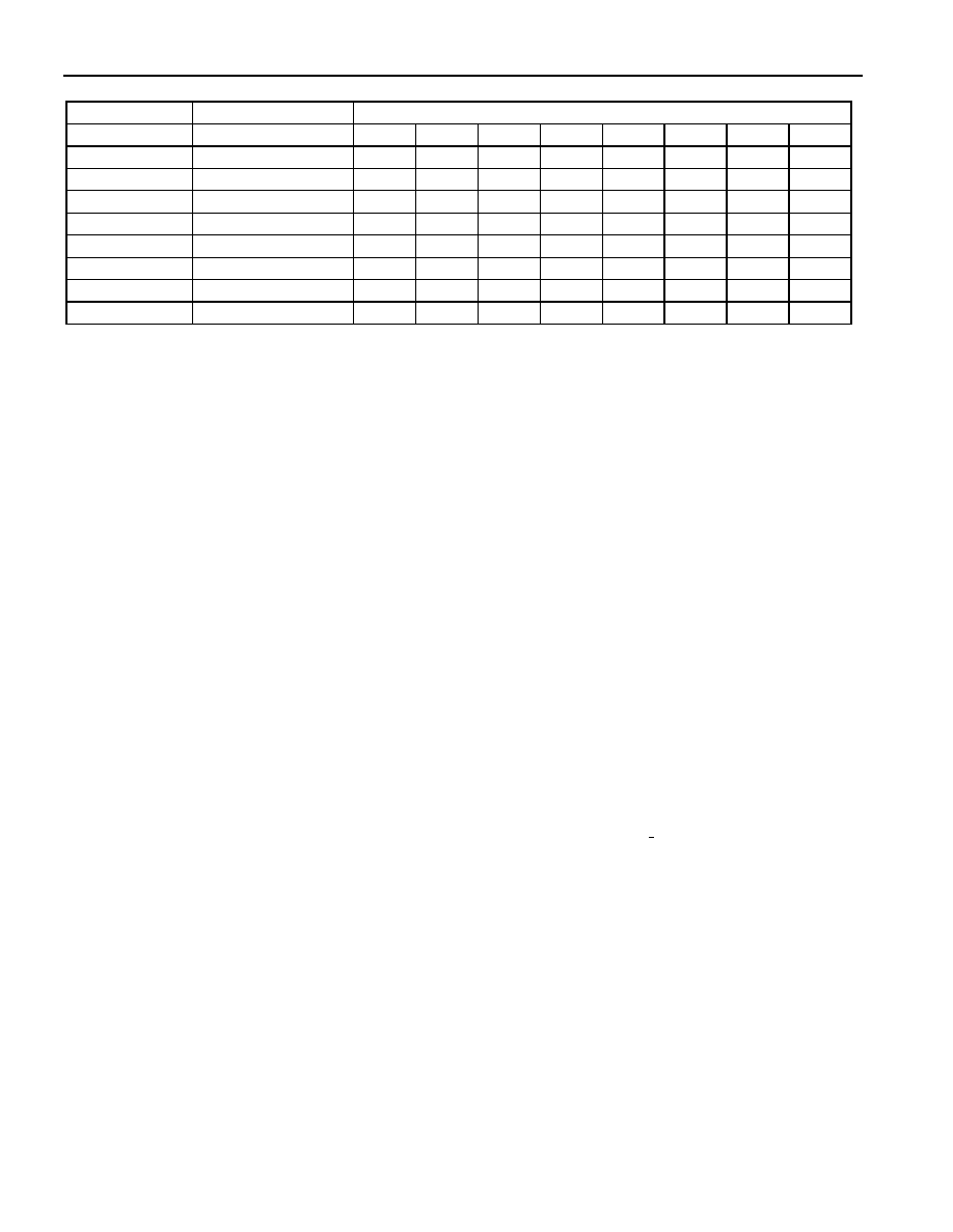
BLOCK SELECTOR CODES OF THE DS1991 Figure 6
Block Nr.
Address Range
LS Byte Codes MS Byte
0 to 7
00 to 3FH
56
56
7F
51
57
5D
5A
7F
0
identifier
9A
9A
B3
9D
64
6E
69
4C
1
password
9A
9A
4C
62
9B
91
69
4C
2
10H to 17H
9A
65
B3
62
9B
6E
96
4C
3
18H to 1FH
6A
6A
43
6D
6B
61
66
43
4
20H to 27H
95
95
BC
92
94
9E
99
BC
5
28H to 2FH
65
9A
4C
9D
64
91
69
B3
6
30H to 37H
65
65
B3
9D
64
6E
96
B3
7
38H to 3FH
65
65
4C
62
9B
91
96
B3
Write SubKey [99H]
The Write Subkey command is used to enter data into the selected subkey. Since the subkeys are secure,
the correct password is required to access them. The sequence begins by reading the ID field; the
password is then written back. If the password is incorrect, the transaction is terminated. Otherwise, the
data following is written into the secure area. The starting address for the write sequence is specified in
the command word. Data can be continuously written until the end of the secure subkey is reached or
until the DS1991 is reset. The command sequence is shown in Figure 5, 2nd page, center column.
Read SubKey [66H]
The Read Subkey command is used to retrieve data from the selected subkey. Since the subkeys are
secure, the correct password is required to access them. The sequence begins by reading the ID field; the
password is then written back. If the password is incorrect, the DS1991 will transmit random data.
Otherwise the data can be read from the subkey. The starting address is specified in the command. Data
can be continuously read until the end of the subkey is reached or until the DS1991 is reset. The
command sequence is shown in Figure 5, 2nd page, left column.
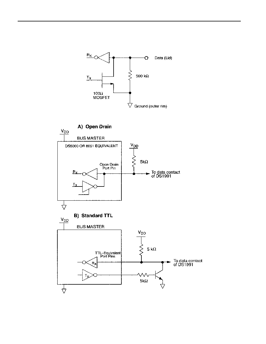
1-WIRE BUS SYSTEM
The 1-Wire bus is a system which has a single bus master and one or more slaves. In all instances, the
DS1991 is a slave device. The bus master is typically a micro-controller. The discussion of this bus
system is broken down into three topics: hardware configuration, transaction sequence, and 1-Wire
signaling (signal types and timing). A 1-Wire protocol defines bus transactions in terms of the bus state
during specified time slots that are initiated on the falling edge of sync pulses from the bus master. For a
more detailed protocol description, refer to Chapter 4 of the Book of DS19xx iButton Standards.
HARDWARE CONFIGURATION
The 1- bus has only a single line by definition; it is important that each device on the bus be able to drive
it at the appropriate time. To facilitate this, each device attached to the 1-Wire bus must have an open
drain connections or 3-state outputs. The DS1991 is an open drain part with an internal circuit equivalent
to that shown in Figure 7. The bus master can be the same equivalent circuit. If a bidirectional pin is not
available, separate output and input pins can be tied together.
The bus master requires a pullup resistor at the master end of the bus, with the bus master circuit
equivalent to the one shown in Figures 8a and 8b. The value of the pullup resistor should be
approximately 5 k
for short line lengths.
A multidrop bus consists of a 1-Wire bus with multiple slaves attached. The 1-Wire bus has a maximum
data rate of 16.3k bits per second. The idle state for the 1-Wire bus is high. If, for any reason a transaction
DS1991
8 of 14
needs to be suspended, the bus MUST be left in the idle state if the transaction is to resume. If this does
not occur, and the bus is left low for more than 120
µ
s, one or more of the devices on the bus may be
reset.
EQUIVALENT CIRCUIT Figure 7
BUS MASTER CIRCUIT Figure 8

DS1991
9 of 14
TRANSACTION SEQUENCE
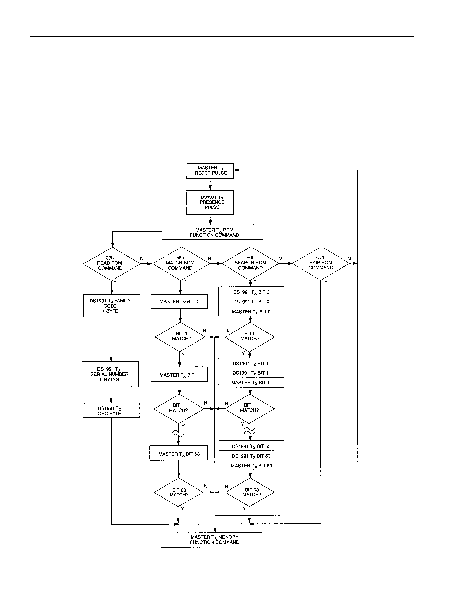
The protocol for accessing the DS1991 via the 1-Wire port is as follows:
§
Initialization
§
ROM Function Command
§
Memory Function Command
§
Transaction/Data
INITIALIZATION
All transactions on the 1-Wire bus begin with an initialization sequence. The initialization sequence
consists of a reset pulse transmitted by the bus master followed by presence pulse(s) transmitted by the
slave(s). The presence pulse lets the bus master know that the DS1991 is on the bus and is ready to
operate. For more details, see the "1-Wire Signaling" section
ROM FUNCTION COMMANDS
Once the bus master has detected a presence pulse, it can issue one of the four ROM function commands.
All ROM function commands are eight bits long. A list of these commands follows (refer to flowchart in
Figure 9).
Read ROM [33H]
This command allows the bus master to read the DS1991's 8-bit family code, unique 48-bit serial number
and 8-bit CRC. This command can be used only if there is a single DS1991 on the bus. If more than one
slave is present on the bus, a data collision will occur when all slaves try to transmit at the same time
(open drain will produce a wired-AND result).
Match ROM [55H]
The match ROM command, followed by a 64-bit ROM sequence, allows the bus master to address a
specific DS1991 on a multidrop bus. Only the DS1991 that exactly matches the 64-bit ROM sequence
will respond to the subsequent memory function command. All slaves that do not match the 64-bit ROM
sequence will wait for a reset pulse. This command can be used with a single or multiple devices on the
bus.
Skip ROM [CCH]
This command can save time in a single drop bus system by allowing the bus master to access the
memory functions without providing the 64-bit ROM code. If more than one slave is present on the bus
and a read command is issued following the Skip ROM command, data collision will occur on the bus as
multiple slaves transmit simultaneously (open drain will produce a wired-AND result).
Search ROM [F0H]
When a system is initially brought up, the bus master might not know the number of devices on the 1-
Wire bus or their 64-bit ROM codes. The Search ROM command allows the bus master to use a process
of elimination to identify the 64-bit ROM codes of all slave devices on the bus. The ROM search process
is the repetition of a simple 3-step routine: read a bit, read the complement of the bit, then write the
desired value of that bit. The bus master performs this simple 3-step routine on each bit of the ROM.
After one complete pass, the bus master knows the contents of the ROM in one device. The remaining
number of devices and their ROM codes may be identified by additional passes. See Chapter 5 of the
Book of DS19xx iButton Standards for a comprehensive discussion of a search ROM, including an actual
example.
DS1991
10 of 14
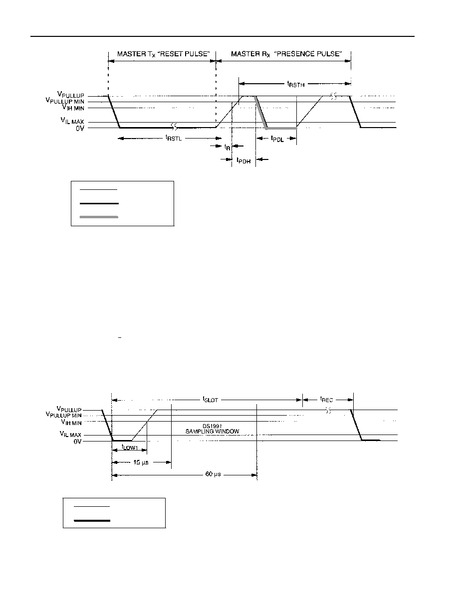
1-WIRE SIGNALING
The DS1991 requires strict protocols to ensure data integrity. The protocol consists of four types of
signaling on one line: Reset Sequence with Reset Pulse and Presence Pulse, Write 0, Write 1 and Read
Data. All these signals except presence pulse are initiated by the bus master. The initialization sequence
required to begin any communication with the DS1991 is shown in Figure 10. A reset pulse followed by a
presence pulse indicates the DS1991 is ready to send or receive data given the correct ROM command
and memory function command. The bus master transmits (TX) a reset pulse (t
RSTL
, minimum 480
µ
s).
The bus master then releases the line and goes into receive mode (RX). The 1-Wire bus is pulled to a high
state via the pullup resistor. After detecting the rising edge on the data pin, the DS1991 waits (t
PDH
, 15-60
µ
s) and then transmits the presence pulse (t
PDL
, 60-240
µ
s).
ROM FUNCTIONS FLOW CHART Figure 9
DS1991
11 of 14
INITIALIZATION PROCEDURE "RESET AND PRESENCE PULSES" Figure 10
480
µ
s
t
RSTL
<
*
480
µ
s
t
RSTH
<
(includes recovery time)
15
µ
s
t
PDH
< 60
µ
s
60
µ
s
t
PDL
< 240
µ
s
In order not to mask interrupt signaling by other devices on the 1-Wire bus, t
RSTL
+ t
R
should always
be less than 960
µ
s.
READ/WRITE TIME SLOTS
The definitions of write and read time slots are illustrated in Figure 11. All time slots are initiated by the
master driving the data line low. The falling edge of the data line synchronizes the DS1991 to the master
by triggering a delay circuit in the DS1991. During write time slots, the delay circuit determines when the
DS1991 will sample the data line. For a read data time slot, if a "0" is to be transmitted, the delay circuit
determines how long the DS1991 will hold the data line low overriding the 1 generated by the master. If
the data bit is a "1", the iButton will leave the read data time slot unchanged.
READ/WRITE TIMING DIAGRAM Figure 11
Write-One Time Slot
60
µ
s
t
SLOT
< 120
µ
s
1
µ
s
t
LOW1
< 15
µ
s
1
µ
s
t
REC
<
RESISTOR
MASTER
RESISTOR
MASTER
DS1991

DS1991
12 of 14
READ/WRITE TIMING DIAGRAM (cont'd) Figure 11
Write-Zero Time Slot
60
µ
s < t
LOW0
< t
SLOT
< 120
µ
s
1
µ
s < t
REC
<
Read-Data Time Slot
60
µ
s
t
SLOT
< 120
µ
s
1
µ
s
t
LOWR
< 15
µ
s
0
t
RELEASE
< 45
µ
s
1
µ
s
t
REC
<
t
RDV
= 15
µ
s
t
SU
< 1
µ
s
RESISTOR
MASTER
DS1991

DS1991
13 of 14
PHYSICAL SPECIFICATIONS
Size
See mechanical drawing
Weight
3.3 grams
Humidity
90% RH at 50°C
Altitude
10,000 feet
Expected Service Life
10 years at 25°C (150 million transactions, see note 4)
Safety
Meets UL#913 (4th Edit.); Intrinsically Safe Apparatus,
Approved under Entity Concept for use in Class I, Division
1, Group A, B, C and D Locations
ABSOLUTE MAXIMUM RATINGS*
Voltage on any Pin Relative to Ground
-0.5V to +7.0V
Operating Temperature
-40°C to +70°C
Storage Temperature
-40°C to +70°C
This is a stress rating only and functional operation of the device at these or any other conditions
above those indicated in the operation sections of this specification is not implied. Exposure to
absolute maximum rating conditions for extended periods of time may affect reliability.
DC ELECTRICAL CHARACTERISTICS (V
PUP
*=2.8V to 6.0V; -40
°
C to +70
°
C)
PARAMETER
SYMBOL MIN
TYP
MAX
UNITS
NOTES
Input Logic Low
V
IL
-0.3
0.8
V
1
Input Logic High
V
IH
2.2
6.0
V
Output Logic Low @ 4 mA
V
OL
0.4
V
Output Logic High
V
OH
V
PUP
6.0
V
1,2
Input Resistance
V
IL
500
k
3
* V
PUP
= external pullup voltage
AC ELECTRICAL CHARACTERISTICS
(-40°C to 70°C)
PARAMETER
SYMBOL MIN
TYP
MAX
UNITS
NOTES
Time Slot Period
t
SLOT
60
120
µ
s
Write 1 Low Time
t
LOW1
1
15
µ
s
Write 0 Low Time
t
LOW0
60
120
µ
s
Read Data Valid
t
RDV
exactly 15
µ
s
Release Time
t
RELEASE
0
15
45
µ
s
Read Data Setup
t
SU
1
µ
s
5
Recovery Time
t
REC
1
µ
s
Reset Low Time
t
RSTL
480
µ
s
Reset High Time
t
RSTH
480
µ
s
4
Presence Detect High
t
PDH
15
60
µ
s
Presence Detect Low
t
PDL
60
240
µ
s

DS1991
14 of 14
NOTES:
1.
All voltages are referenced to ground.
2.
V
PUP
= external pullup voltage to system supply.
3.
Input pulldown resistance to ground.
4.
An additional reset or communication sequence cannot begin until the reset high time has expired.
5.
Read data setup time refers to the time the host must pull the 1-Wire bus low to read a bit. Data is
guaranteed to be valid within 1
µ
s of this falling edge and will remain valid for 14
µ
s minimum. (15
µ
s total from falling edge on 1-Wire bus.)