1 of 27
050400
FEATURES
Unique 1Wire interface requires only one
port pin for communication
Multidrop capability simplifies distributed
temperature sensing applications
Requires no external components
Can be powered from data line. Power supply
range is 3.0V to 5.5V
Zero standby power required
Measures temperatures from 55°C to
+125°C. Fahrenheit equivalent is 67°F to
+257°F
±
0.5
°
C accuracy from 10°C to +85°C
Temperature is read as a 9bit digital value
Converts temperature to digital word in
750 ms (max.)
Userdefinable, nonvolatile temperature
alarm settings
Alarm search command identifies and
addresses devices whose temperature is
outside of programmed limits (temperature
alarm condition)
Functionally compatible with DS1820 1-Wire
digital thermometer
Applications include thermostatic controls,
industrial systems, consumer products,
thermometers, or any thermally sensitive
system
PIN ASSIGNMENT
PIN DESCRIPTION
GND - Ground
DQ
- Data In/Out
V
DD
- Power Supply Voltage
NC
- No Connect
DESCRIPTION
The DS18S20 Digital Thermometer provides 9bit temperature readings which indicate the temperature
of the device.
Information is sent to/from the DS18S20 over a 1Wire interface, so that only one wire (and ground)
needs to be connected from a central microprocessor to a DS18S20. Power for reading, writing, and
performing temperature conversions can be derived from the data line itself with no need for an external
power source.
Because each DS18S20 contains a unique silicon serial number, multiple DS18S20s can exist on the
same 1Wire bus. This allows for placing temperature sensors in many different places. Applications
where this feature is useful include HVAC environmental controls, sensing temperatures inside buildings,
equipment or machinery, and process monitoring and control.
DS18S20
High Precision
1-Wire
®
Digital Thermometer
www.dalsemi.com
PRELIMINARY
DALLAS
DS18S20
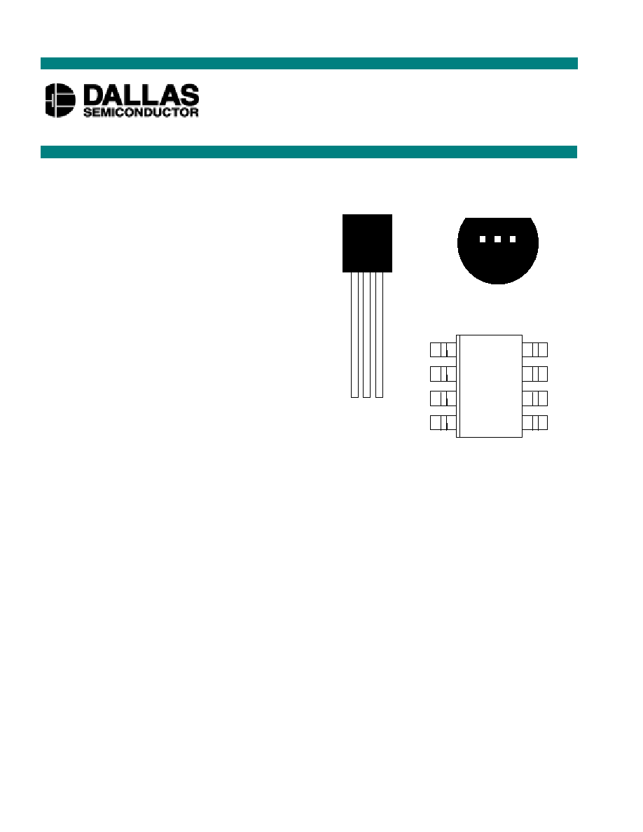
1 2 3
GND
DQ
VDD
1 2 3
BOTTOM VIEW
DS18S20 To-92
Package
1
2
3
4
8
7
6
5
NC
NC
NC
GND
NC
NC
V
DD
DQ
DS18S20Z
8-Pin SOIC (150 mil)

DS18S20
2 of 27
DETAILED PIN DESCRIPTION
PIN
8-PIN SOIC
PIN
TO92
SYMBOL
DESCRIPTION
5
1
GND
Ground.
4
2
DQ
Data Input/Output pin. For 1-Wire operation: Open drain.
(See "Parasite Power" section.)
3
3
V
DD
Optional V
DD
pin. See "Parasite Power" section for details of
connection. V
DD
must be grounded for operation in parasite
power mode.
DS18S20Z (8-pin SOIC): All pins not specified in this table are not to be connected.
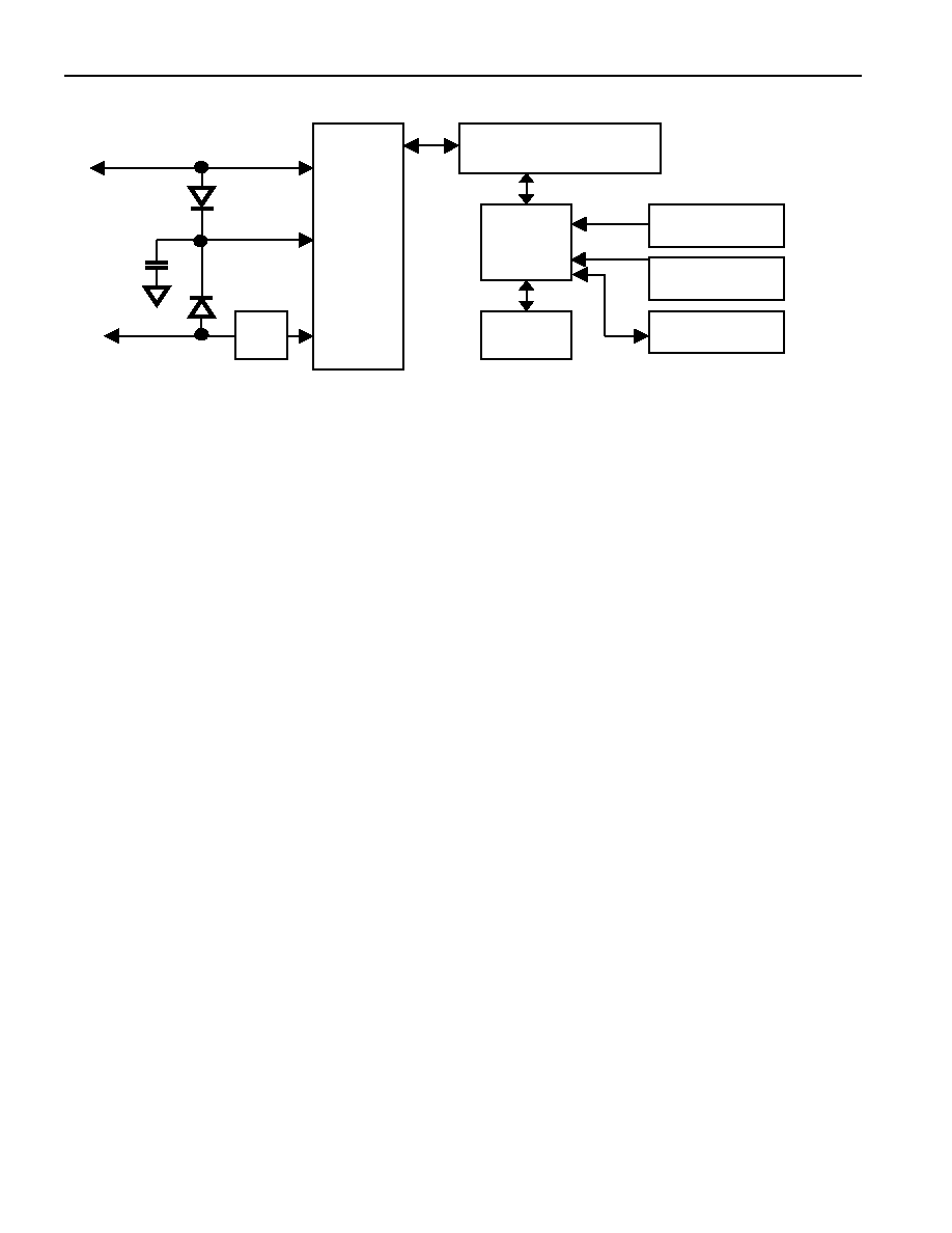
OVERVIEW
The block diagram of Figure 1 shows the major components of the DS18S20. The DS18S20 has three
main data components: 1) 64bit lasered ROM, 2) temperature sensor, 3) nonvolatile temperature alarm
triggers TH and TL. The device derives its power from the 1Wire communication line by storing energy
on an internal capacitor during periods of time when the signal line is high and continues to operate off
this power source during the low times of the 1Wire line until it returns high to replenish the parasite
(capacitor) supply. As an alternative, the DS18S20 may also be powered from an external 3 volt 5 volt
supply.
Communication to the DS18S20 is via a 1Wire port. With the 1Wire port, the memory and control
functions will not be available before the ROM function protocol has been established. The master must
first provide one of five ROM function commands: 1) Read ROM, 2) Match ROM, 3) Search ROM, 4)
Skip ROM, or 5) Alarm Search. These commands operate on the 64bit lasered ROM portion of each
device and can single out a specific device if many are present on the 1Wire line as well as indicate to
the bus master how many and what types of devices are present. After a ROM function sequence has
been successfully executed, the memory and control functions are accessible and the master may then
provide any one of the six memory and control function commands.
One control function command instructs the DS18S20 to perform a temperature measurement. The result
of this measurement will be placed in the DS18S20's scratch-pad memory, and may be read by issuing a
memory function command which reads the contents of the scratchpad memory. The temperature alarm
triggers TH and TL consist of 1-byte EEPROM each. If the alarm search command is not applied to the
DS18S20, these registers may be used as general purpose user memory. Writing TH and TL is done
using a memory function command. Read access to these registers is through the scratchpad. All data is
read and written least significant bit first.
DS18S20
3 of 27
DS18S20 BLOCK DIAGRAM Figure 1
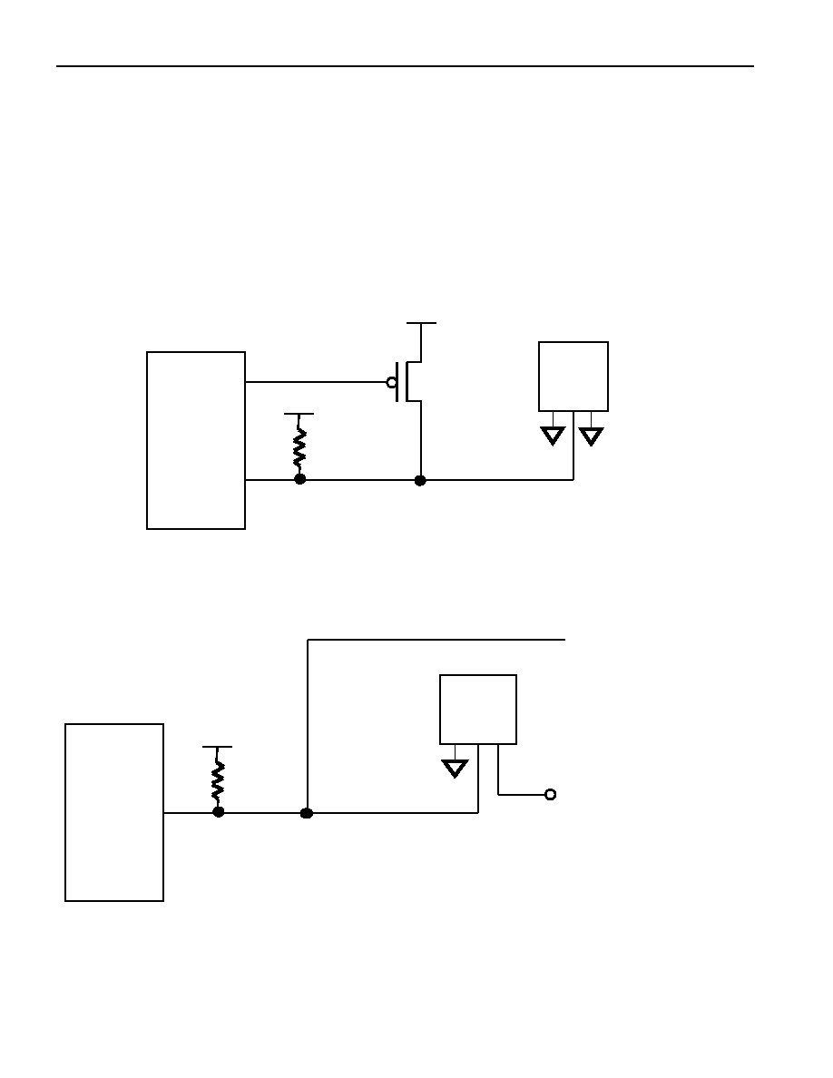
PARASITE POWER
The block diagram (Figure 1) shows the parasite-powered circuitry. This circuitry "steals" power
whenever the DQ or V
DD
pins are high. DQ will provide sufficient power as long as the specified timing
and voltage requirements are met (see the section titled "1Wire Bus System"). The advantages of
parasite power are twofold: 1) by parasiting off this pin, no local power source is needed for remote
sensing of temperature, and 2) the ROM may be read in absence of normal power.
In order for the DS18S20 to be able to perform accurate temperature conversions, sufficient power must
be provided over the DQ line when a temperature conversion is taking place. Since the operating current
of the DS18S20 is up to 1.5 mA, the DQ line will not have sufficient drive due to the 5k pullup resistor.
This problem is particularly acute if several DS18S20s are on the same DQ and attempting to convert
simultaneously.
There are two ways to assure that the DS18S20 has sufficient supply current during its active conversion
cycle. The first is to provide a strong pullup on the DQ line whenever temperature conversions or copies
to the E
2
memory are taking place. This may be accomplished by using a MOSFET to pull the DQ line
directly to the power supply as shown in Figure 2. The DQ line must be switched over to the strong
pull-up within 10
µ
s maximum after issuing any protocol that involves copying to the E
2
memory or
initiates temperature conversions. When using the parasite power mode, the V
DD
pin must be tied to
ground.
Another method of supplying current to the DS18S20 is through the use of an external power supply tied
to the V
DD
pin, as shown in Figure 3. The advantage to this is that the strong pullup is not required on the
DQ line, and the bus master need not be tied up holding that line high during temperature conversions.
This allows other data traffic on the 1Wire bus during the conversion time. In addition, any number of
DS18S20s may be placed on the 1Wire bus, and if they all use external power, they may all
simultaneously perform temperature conversions by issuing the Skip ROM command and then issuing the
Convert T command. Note that as long as the external power supply is active, the GND pin may not be
floating.
The use of parasite power is not recommended above 100
°
C, since it may not be able to sustain
communications given the higher leakage currents the DS18S20 exhibits at these temperatures. For
applications in which such temperatures are likely, it is strongly recommended that V
DD
be applied to the
DS18S20.
POWER
SUPPLY
SENSE
64-BIT ROM
AND
1-WIRE PORT
MEMORY AND
CONTROL LOGIC
SCRATCHPAD
8-BIT CRC
GENERATOR
TEMPERATURE
SENSOR
HIGH TEMPERATURE
TRIGGER, TH
LOW TEMPERATURE
TRIGGER, TH
DQ
V
DD
INTERNAL V
DD
DS18S20
4 of 27
For situations where the bus master does not know whether the DS18S20s on the bus are parasite
powered or supplied with external V
DD
, a provision is made in the DS18S20 to signal the power supply
scheme used. The bus master can determine if any DS18S20s are on the bus which require the strong
pullup by sending a Skip ROM protocol, then issuing the read power supply command. After this
command is issued, the master then issues read time slots. The DS18S20 will send back "0" on the
1-Wire bus if it is parasite powered; it will send back a "1" if it is powered from the V
DD
pin. If the
master receives a "0," it knows that it must supply the strong pullup on the DQ line during temperature
conversions. See "Memory Command Functions" section for more detail on this command protocol.
STRONG PULL-UP FOR SUPPLYING DS18S20 DURING TEMPERATURE
CONVERSION Figure 2
USING V
DD
TO SUPPLY TEMPERATURE CONVERSION CURRENT
Figure 3
+3V - +5V
DS18S20
+3V - +5V
4.7k
GND
V
DD
I/O
µ
µ
µ
µ
P
+3V - +5V
4.7k
µ
µ
µ
µ
P
DS18S20
GND
V
DD
I/O
TO OTHER
1-WIRE DEVICES
EXTERNAL +3V - +5V
SUPPLY
DS18S20
5 of 27
OPERATION MEASURING TEMPERATURE
The core functionality of the DS18S20 is its direct-to-digital temperature sensor. The direct readout of
temperature data is 9 bits wide, equating to a resolution of 0.5
°
C; if higher resolution is desired, an
algorithm is described later in this section to achieve that need. Following the issuance of the Convert T
[44h] command, a temperature conversion is performed and the thermal data is stored in the scratchpad
memory in a 16-bit, sign-extended two's complement format. The temperature information can be
retrieved over the 1-Wire interface by issuing a Read Scratchpad [BEh] command once the conversion
has been performed. The data is transferred over the 1-Wire bus, LSB first. The MSB of the temperature
register contains the "sign" (S) bit, denoting whether the temperature is positive or negative.
Table 2 describes the exact relationship of output data to measured. For Fahrenheit usage, a lookup table
or conversion routine must be used.
Temperature/Data Relationships Table 2
2
6
2
5
2
4
2
3
2
2
2
1
2
0
2
-1
LSB
MSb
(unit =
°
C)
LSb
S
S
S
S
S
S
S
S
MSB
TEMPERATURE
DIGITAL OUTPUT
(Binary)
DIGITAL
OUTPUT
(Hex)
+85°C
0000 0101 0101 0000
0550h*
+125°C
0000 0000 1111 1010
00FAh
+25.0°C
0000 0000 0011 0010
0032h
+0.5°C
0000 0000 0000 0001
0001h
0°C
0000 0000 0000 0000
0000h
-0.5°C
1111 1111 1111 1111
FFFFh
-25.0°C
1111 1111 1100 1110
FFCEh
-55°C
1111 1111 1001 0010
FF92h
*The power on reset register value is +85°C
Higher resolutions may be obtained by the following procedure. First, read the temperature,
COUNT_REMAIN, and COUNT_PER_C registers from the scratchpad. Truncate the 0.5
°
C bit (the
LSB) from the temperature value. This value is TEMP_READ. The actual temperature may then be
calculated by using the following:
C
PER
COUNT
REMAIN
COUNT
C
PER
COUNT
READ
TEMP
E
TEMPERATUR
_
_
_
_
_
25
.
0
_
-
+
-
=
OPERATION ALARM SIGNALING
After the DS18S20 has performed a temperature conversion, the temperature value is compared to the
trigger values stored in TH and TL. Since these registers are 8bit only, the 0.5
°
C bit is ignored for
comparison. The most significant bit of TH or TL directly corresponds to the sign bit of the 16bit
temperature register. If the result of a temperature measurement is higher than TH or lower than TL, an
alarm flag inside the device is set. This flag is updated with every temperature measurement. As long as

DS18S20
6 of 27
the alarm flag is set, the DS18S20 will respond to the alarm search command. This allows many
DS18S20s to be connected in parallel doing simultaneous temperature measurements. If somewhere the
temperature exceeds the limits, the alarming device(s) can be identified and read immediately without
having to read nonalarming devices.
64-BIT LASERED ROM
Each DS18S20 contains a unique ROM code that is 64bits long. The first 8 bits are a 1Wire family
code (DS18S20 code is 10h). The next 48 bits are a unique serial number. The last 8 bits are a CRC of
the first 56 bits. (See Figure 4.) The 64bit ROM and ROM Function Control section allow the DS18S20
to operate as a 1Wire device and follow the 1Wire protocol detailed in the section "1Wire Bus
System." The functions required to control sections of the DS18S20 are not accessible until the ROM
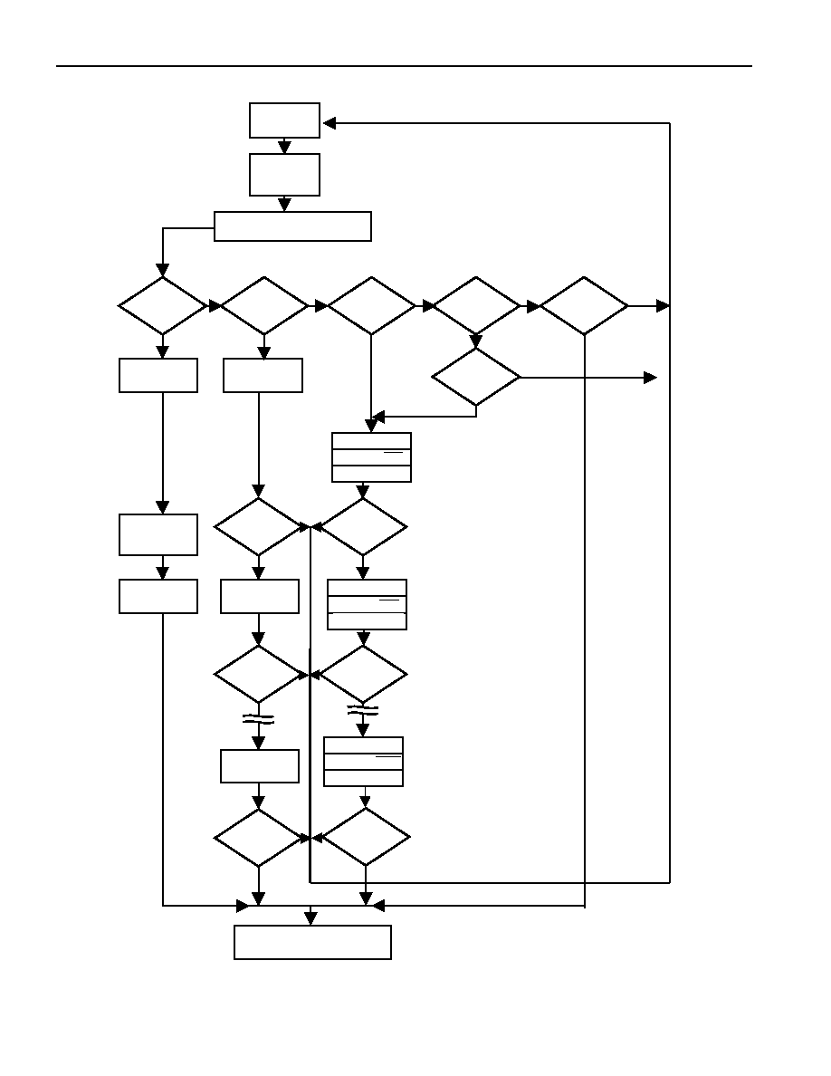
function protocol has been satisfied. This protocol is described in the ROM function protocol flowchart
(Figure 5). The 1Wire bus master must first provide one of five ROM function commands: 1) Read
ROM, 2) Match ROM, 3) Search ROM, 4) Skip ROM, or 5) Alarm Search. After a ROM functions
sequence has been successfully executed, the functions specific to the DS18S20 are accessible and the
bus master may then provide one of the six memory and control function commands.
CRC GENERATION
The DS18S20 has an 8bit CRC stored in the most significant byte of the 64bit ROM. The bus master
can compute a CRC value from the first 56bits of the 64bit ROM and compare it to the value stored
within the DS18S20 to determine if the ROM data has been received errorfree by the bus master. The
equivalent polynomial function of this CRC is:
CRC = X
8
+ X
5
+ X
4
+ 1
The DS18S20 also generates an 8bit CRC value using the same polynomial function shown above and
provides this value to the bus master to validate the transfer of data bytes. In each case where a CRC is
used for data transfer validation, the bus master must calculate a CRC value using the polynomial
function given above and compare the calculated value to either the 8bit CRC value stored in the 64bit
ROM portion of the DS18S20 (for ROM reads) or the 8bit CRC value computed within the DS18S20
(which is read as a ninth byte when the scratchpad is read). The comparison of CRC values and decision
to continue with an operation are determined entirely by the bus master. There is no circuitry inside the
DS18S20 that prevents a command sequence from proceeding if the CRC stored in or calculated by the
DS18S20 does not match the value generated by the bus master.
The 1Wire CRC can be generated using a polynomial generator consisting of a shift register and XOR
gates as shown in Figure 6. Additional information about the Dallas 1Wire Cyclic Redundancy Check is
available in Application Note 27 entitled "Understanding and Using Cyclic Redundancy Checks with
Dallas Semiconductor Touch Memory Products."
The shift register bits are initialized to "0". Then starting with the least significant bit of the family code,
one bit at a time is shifted in. After the eighth bit of the family code has been entered, then the serial
number is entered. After the 48
th
bit of the serial number has been entered, the shift register contains the
CRC value. Shifting in the 8 bits of CRC should return the shift register to all "0s".
64-BIT LASERED ROM Figure 4
8-BIT CRC CODE
48-BIT SERIAL NUMBER
8-BIT FAMILY CODE (10h)
MSB
MSB
LSB
LSB
LSB
MSB
DS18S20
7 of 27
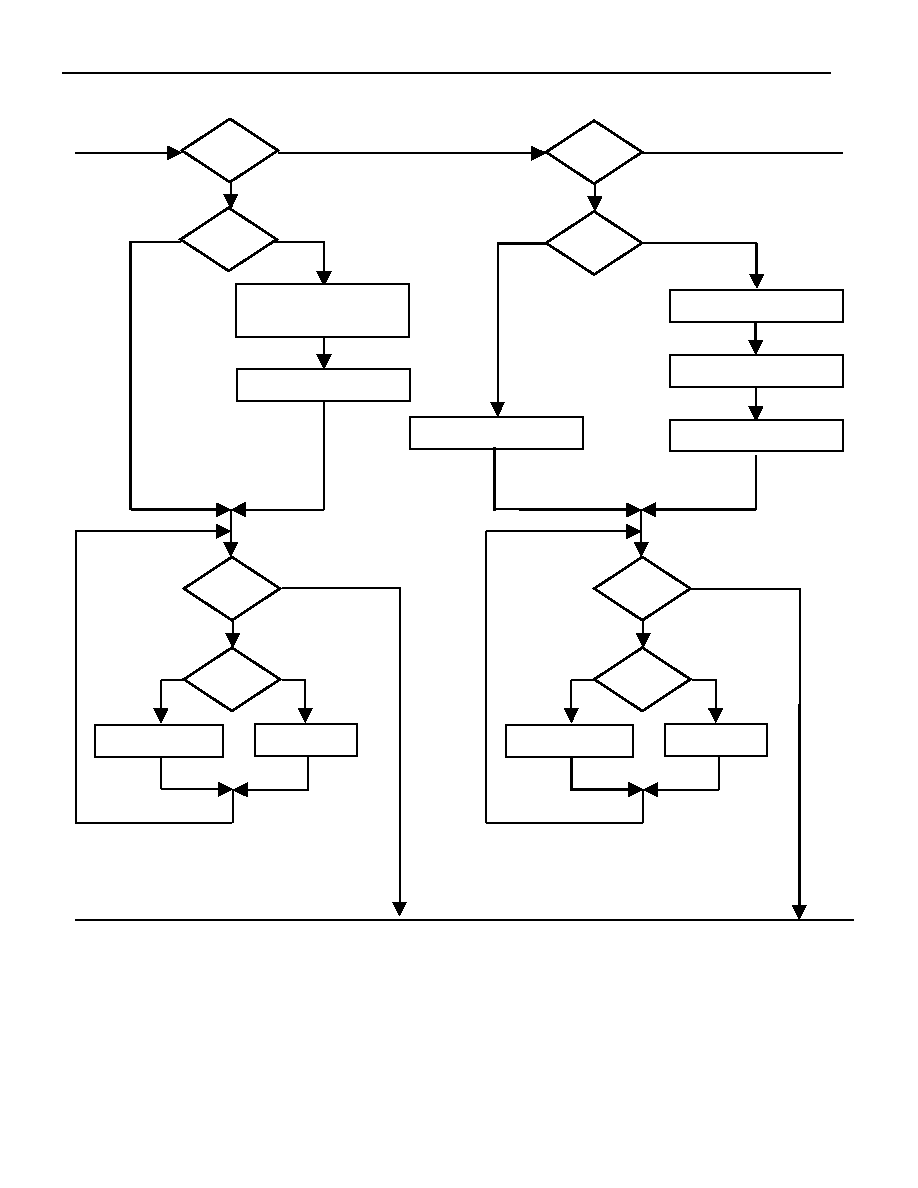
ROM FUNCTIONS FLOW CHART Figure 5
CCh
SKIP ROM
COMMAND
DS18S20 T
X
FAMILY CODE
1 BYTE
DS18S20 T
X
SERIAL NUMBER
6 BYTES
MASTER T
X
RESET PULSE
DS18S20 T
X
PRESENCE
PULSE
MASTER T
X
ROM
FUNCTION COMMAND
33h
READ ROM
COMMAND
55h
MATCH ROM
COMMAND
F0h
SEARCH ROM
COMMAND
ECh
ALARM
SEARCH
COMMAND
ALARM
CONDITION ?
MASTER T
X
BIT 0
DS18S20 T
X
BIT 0
DS18S20 T
X
BIT 0
MASTER T
X
BIT 0
DS18S20 T
X
BIT 1
DS18S20 T
X
BIT 1
MASTER T
X
BIT 1
DS18S20 T
X
BIT 63
DS18S20 T
X
BIT 63
MASTER T
X
BIT 63
BIT 0
MATCH?
BIT 0
MATCH?
DS18S20 T
X
CRC BYTE
MASTER T
X
BIT 1
BIT 1
MATCH?
BIT 1
MATCH?
BIT 63
MATCH?
BIT 63
MATCH?
MASTER T
X
BIT 63
N
Y
Y
Y
Y
Y
N
N
N
N
N
N
N
N
N
N
N
Y
Y
Y
Y
Y
Y
Y
MASTER T
X
MEMORY OR CONTROL
FUNCTION COMMAND
DS18S20
8 of 27
1-WIRE CRC CODE Figure 6
MEMORY
The DS18S20's memory is organized as shown in Figure 7. The memory consists of a scratchpad RAM
and a nonvolatile, electrically erasable (E
2
) RAM, which stores the high and low temperature triggers, TH
and TL. The scratchpad helps insure data integrity when communicating over the 1Wire bus. Data is
first written to the scratchpad where it can be read back. After the data has been verified, a copy
scratchpad command will transfer the data to the nonvolatile (E
2
) RAM. This process insures data
integrity when modifying the memory. The DS18S20 EEPROM is rated for a minimum of 50,000 writes
and 10 years data retention at T = +55°C.
The scratchpad is organized as 8 bytes of memory. The first 2-bytes contain the measured temperature
information. The third and fourth bytes are volatile copies of TH and TL and are refreshed with every
poweron reset. The next 2 bytes are not used; upon reading back, however, they will appear as all logic
"1s". The seventh and eighth bytes are count registers, which may be used in obtaining higher
temperature resolution (see "Operationmeasuring Temperature" section). There is a ninth byte which
may be read with a Read Scratchpad command. This byte contains a cyclic redundancy check (CRC)
byte which is the CRC over all of the 8 previous bytes. This CRC is implemented in the fashion
described in the section titled "CRC Generation."
DS18S20 MEMORY MAP Figure 7
TEMPERATURE LSB
TEMPERATURE MSB
TH/USER BYTE 1
TL/USER BYTE 2
RESERVED
COUNT REMAIN
COUNT PER °C
CRC
TH/USER BYTE 1
TL/USER BYTE 2
RESERVED
SCRATCHPAD
BYTE
0
1
2
3
4
5
6
7
8
E
2
RAM
(MSB)
(LSB)
XOR
XOR
XOR
INPUT
DS18S20
9 of 27
1-WIRE BUS SYSTEM
The 1Wire bus is a system which has a single bus master and one or more slaves. The DS18S20
behaves as a slave. The discussion of this bus system is broken down into three topics: hardware
configuration, transaction sequence, and 1Wire signaling (signal types and timing).
HARDWARE CONFIGURATION
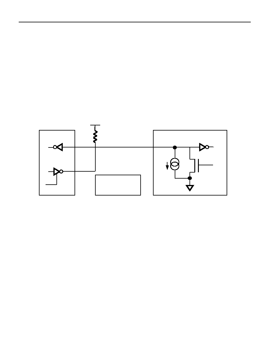
The 1Wire bus has only a single line by definition; it is important that each device on the bus be able to
drive it at the appropriate time. To facilitate this, each device attached to the 1Wire bus must have open
drain or 3state outputs. The 1Wire port of the DS18S20 (DQ pin) is open drain with an internal circuit
equivalent to that shown in Figure 8. A multidrop bus consists of a 1Wire bus with multiple slaves
attached. The 1Wire bus requires a pullup resistor of approximately 5 k
.
HARDWARE CONFIGURATION Figure 8
The idle state for the 1Wire bus is high. If for any reason a transaction needs to be suspended, the bus
MUST be left in the idle state if the transaction is to resume. Infinite recovery time can occur between
bits so long as the 1Wire bus is in the inactive (high) state during the recovery period. If this does not
occur and the bus is left low for more than 480
µ
s, all components on the bus will be reset.
TRANSACTION SEQUENCE
The protocol for accessing the DS18S20 via the 1Wire port is as follows:
·
Initialization
·
ROM Function Command
·
Memory Function Command
·
Transaction/Data
+3V - +5V
4.7k
5 µA
Typ.
R
X
T
X
DS18S20 1-WIRE PORT
100
MOSFET
T
X
R
X
R
X
= RECEIVE
T
X
= TRANSMIT
BUS MASTER

DS18S20
10 of 27
INITIALIZATION
All transactions on the 1Wire bus begin with an initialization sequence. The initialization sequence
consists of a reset pulse transmitted by the bus master followed by presence pulse(s) transmitted by the
slave(s).
The presence pulse lets the bus master know that the DS18S20 is on the bus and is ready to operate. For
more details, see the "1Wire Signaling" section.
ROM FUNCTION COMMANDS
Once the bus master has detected a presence, it can issue one of the five ROM function commands. All
ROM function commands are 8 bits long. A list of these commands follows (refer to flowchart in
Figure 5):
Read ROM [33h]
This command allows the bus master to read the DS18S20's 8bit family code, unique 48bit serial
number, and 8bit CRC. This command can only be used if there is a single DS18S20 on the bus. If
more than one slave is present on the bus, a data collision will occur when all slaves try to transmit at the
same time (open drain will produce a wired AND result).
Match ROM [55h]
The match ROM command, followed by a 64bit ROM sequence, allows the bus master to address a
specific DS18S20 on a multidrop bus. Only the DS18S20 that exactly matches the 64bit ROM sequence
will respond to the following memory function command. All slaves that do not match the 64bit ROM
sequence will wait for a reset pulse. This command can be used with a single or multiple devices on the
bus.
Skip ROM [CCh]
This command can save time in a single drop bus system by allowing the bus master to access the
memory functions without providing the 64bit ROM code. If more than one slave is present on the bus
and a Read command is issued following the Skip ROM command, data collision will occur on the bus as
multiple slaves transmit simultaneously (open drain pulldowns will produce a wired AND result).
Search ROM [F0h]
When a system is initially brought up, the bus master might not know the number of devices on the
1-Wire bus or their 64bit ROM codes. The search ROM command allows the bus master to use a
process of elimination to identify the 64bit ROM codes of all slave devices on the bus.
Alarm Search [ECh]
The flowchart of this command is identical to the Search ROM command. However, the DS18S20 will
respond to this command only if an alarm condition has been encountered at the last temperature
measurement. An alarm condition is defined as a temperature higher than TH or lower than TL. The
alarm condition remains set as long as the DS18S20 is powered up, or until another temperature
measurement reveals a nonalarming value. For alarming, the trigger values stored in EEPROM are
taken into account. If an alarm condition exists and the TH or TL settings are changed, another
temperature conversion should be done to validate any alarm conditions.

DS18S20
11 of 27
Example of a ROM Search
The ROM search process is the repetition of a simple threestep routine: read a bit, read the complement
of the bit, then write the desired value of that bit. The bus master performs this simple, threestep routine
on each bit of the ROM. After one complete pass, the bus master knows the contents of the ROM in one
device. The remaining number of devices and their ROM codes may be identified by additional passes.
The following example of the ROM search process assumes four different devices are connected to the
same 1Wire bus. The ROM data of the four devices is as shown:
ROM1
00110101...
ROM2
10101010...
ROM3
11110101...
ROM4
00010001...
The search process is as follows:
1.
The bus master begins the initialization sequence by issuing a reset pulse. The slave devices respond
by issuing simultaneous presence pulses.
2.
The bus master will then issue the Search ROM command on the 1Wire bus.
3.
The bus master reads a bit from the 1Wire bus. Each device will respond by placing the value of the
first bit of their respective ROM data onto the 1Wire bus. ROM1 and ROM4 will place a 0 onto the
1Wire bus, i.e., pull it low. ROM2 and ROM3 will place a 1 onto the 1Wire bus by allowing the
line to stay high. The result is the logical AND of all devices on the line, therefore the bus master
sees a 0. The bus master reads another bit. Since the Search ROM data command is being executed,
all of the devices on the 1Wire bus respond to this second read by placing the complement of the
first bit of their respective ROM data onto the 1Wire bus. ROM1 and ROM4 will place a 1 onto the
1Wire, allowing the line to stay high. ROM2 and ROM3 will place a 0 onto the 1Wire, thus it will
be pulled low. The bus master again observes a 0 for the complement of the first ROM data bit. The
bus master has determined that there are some devices on the 1Wire bus that have a 0 in the first
position and others that have a 1.
The data obtained from the two reads of the threestep routine have the following interpretations:
00
There are still devices attached which have conflicting bits in this position.
01
All devices still coupled have a 0bit in this bit position.
10
All devices still coupled have a 1bit in this bit position.
11
There are no devices attached to the 1Wire bus.
4.
The bus master writes a 0. This deselects ROM2 and ROM3 for the remainder of this search pass,
leaving only ROM1 and ROM4 connected to the 1Wire bus.
5.
The bus master performs two more reads and receives a 0bit followed by a 1bit. This indicates that
all devices still coupled to the bus have 0s as their second ROM data bit.
6.
The bus master then writes a 0 to keep both ROM1 and ROM4 coupled.
7.
The bus master executes two reads and receives two 0bits. This indicates that both 1bits and 0bits
exist as the third bit of the ROM data of the attached devices.

DS18S20
12 of 27
8.
The bus master writes a 0bit. This deselects ROM1, leaving ROM4 as the only device still
connected.
9.
The bus master reads the remainder of the ROM bits for ROM4 and continues to access the part if
desired. This completes the first pass and uniquely identifies one part on the 1Wire bus.
10.
The bus master starts a new ROM search sequence by repeating steps 1 through 7.
11.
The bus master writes a 1bit. This decouples ROM4, leaving only ROM1 still coupled.
12.
The bus master reads the remainder of the ROM bits for ROM1 and communicates to the underlying
logic if desired. This completes the second ROM search pass, in which another of the ROMs was
found.
13.
The bus master starts a new ROM search by repeating steps 1 through 3.
14.
The bus master writes a 1bit. This deselects ROM1 and ROM4 for the remainder of this search pass,
leaving only ROM2 and ROM3 coupled to the system.
15.
The bus master executes two Read time slots and receives two 0s.
16.
The bus master writes a 0bit. This decouples ROM3, leaving only ROM2.
17.
The bus master reads the remainder of the ROM bits for ROM2 and communicates to the underlying
logic if desired. This completes the third ROM search pass, in which another of the ROMs was
found.
18.
The bus master starts a new ROM search by repeating steps 13 through 15.
19.
The bus master writes a 1bit. This decouples ROM2, leaving only ROM3.
20.
The bus master reads the remainder of the ROM bits for ROM3 and communicates to the underlying
logic if desired. This completes the fourth ROM search pass, in which another of the ROMs was
found.
NOTE:
The bus master learns the unique ID number (ROM data pattern) of one 1Wire device on each ROM
Search operation. The time required to derive the part's unique ROM code is:
960
µ
s + (8 + 3 x 64) 61
µ
s = 13.16 ms
The bus master is therefore capable of identifying 75 different 1Wire devices per second.
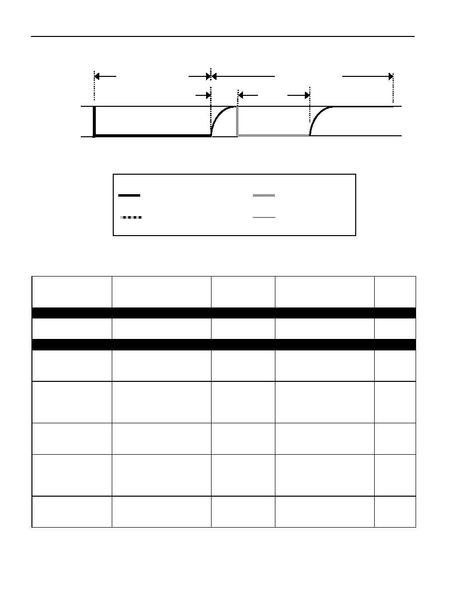
I/O SIGNALING
The DS18S20 requires strict protocols to insure data integrity. The protocol consists of several types of
signaling on one line: reset pulse, presence pulse, write 0, write 1, read 0, and read 1. All of these signals,
with the exception of the presence pulse, are initiated by the bus master.

DS18S20
13 of 27
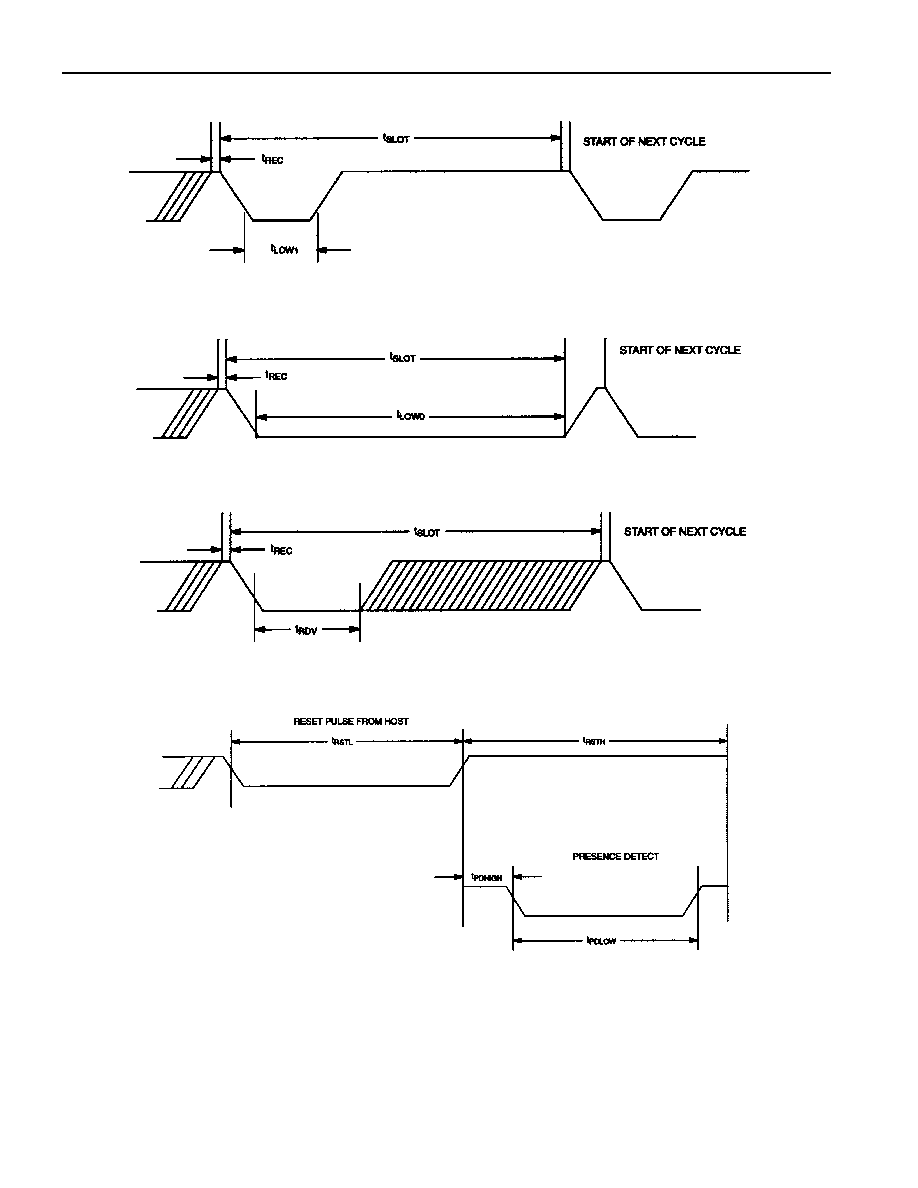
The initialization sequence required to begin any communication with the DS18S20 is shown in Figure
10. A reset pulse followed by a presence pulse indicates the DS18S20 is ready to send or receive data
given the correct ROM command and memory function command.
The bus master transmits (TX) a reset pulse (a low signal for a minimum of 480 ms). The bus master
then releases the line and goes into a receive mode (RX). The 1Wire bus is pulled to a high state via the
5k pullup resistor. After detecting the rising edge on the DQ pin, the DS18S20 waits 1560
µ
s and then
transmits the presence pulse (a low signal for 60240
µ
s).
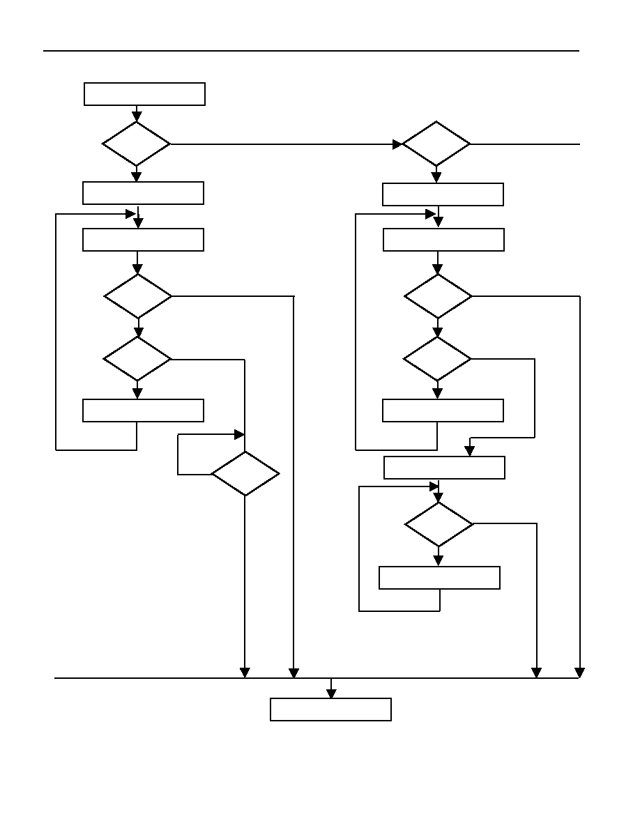
MEMORY COMMAND FUNCTIONS
The following command protocols are summarized in Table 2, and by the flowchart of Figure 9.
Write Scratchpad [4Eh]
This command writes to the scratchpad of the DS18S20, starting at the TH register. The next 2 bytes
written will be saved in scratchpad memory at address locations 2 and 3. Writing may be terminated at
any point by issuing a reset.
Read Scratchpad [BEh]
This command reads the contents of the scratchpad. Reading will commence at byte 0, and will continue
through the scratchpad until the ninth (byte 8, CRC) byte is read. If not all locations are to be read, the
master may issue a reset to terminate reading at any time.
Copy Scratchpad [48h]
This command copies the scratchpad into the E
2
memory of the DS18S20, storing the temperature trigger
bytes in nonvolatile memory. If the bus master issues read time slots following this command, the
DS18S20 will output 0 on the bus as long as it is busy copying the scratchpad to E
2
; it will return a 1
when the copy process is complete. If parasite-powered, the bus master has to enable a strong pullup for
at least 10 ms immediately after issuing this command. The DS18S20 EEPROM is rated for a minimum
of 50,000 writes and 10 years data retention at T = +55°C.
Convert T [44h]
This command begins a temperature conversion. No further data is required. The temperature
conversion will be performed and then the DS18S20 will remain idle. If the bus master issues read time
slots following this command, the DS18S20 will output 0 on the bus as long as it is busy making a
temperature conversion; it will return a 1 when the temperature conversion is complete. If parasite-
powered, the bus master has to enable a strong pullup for a time period greater than t
conv
immediately
after issuing this command.
Recall E2 [B8h]
This command recalls the temperature trigger values stored in E
2
to the scratchpad. This recall operation
happens automatically upon powerup to the DS18S20 as well, so valid data is available in the scratchpad
as soon as the device has power applied. With every read data time slot issued after this command has
been sent, the device will output its temperature converter busy flag: 0=busy, 1=ready.
Read Power Supply [B4h]
With every read data time slot issued after this command has been sent to the DS18S20, the device will
signal its power mode: 0=parasite power, 1=external power supply provided.
DS18S20
14 of 27
MEMORY FUNCTIONS FLOW CHART Figure 9
DS18S20 T
X
SERIAL NUMBER
6 BYTES
Y
N
Y
Y
DS18S20 SETS ADDRESS
COUNTER TO 0
BEh
READ
SCRATCHPAD
?
DS18S20 INCREMENTS
ADDRESS
ADDRESS
=7
?
MASTER
T
X
RESET
?
MASTER R
X
DATA
FROM SCRATCHPAD
N
N
MASTER
T
X
RESET
?
MASTER R
X
8-BIT
CRC OF DATA
N
Y
Y
MASTER
T
X
RESET
?
N
Y
MASTER T
X
MEMORY OR
CONTROL COMMAND
MASTER
T
X
RESET
?
Y
N
N
DS18S20 SETS ADDRESS
COUNTER TO 2
4Eh
WRITE
SCRATCHPAD
?
MASTER T
X
DATA BYTE
TO SCRATCHPAD
DS18S20 INCREMENTS
ADDRESS
ADDRESS
=3
?
N
Y
DS18S20 T
X
PRESENCE PULSE
MASTER RX "1s"
DS18S20
15 of 27
MEMORY FUNCTIONS FLOW CHART Figure 9 (cont'd)
MASTER ENABLES
STRONG PULLUP FOR
10ms
48h
COPY
SCRATCHPAD
?
Y
N
PARASITE
POWER
?
N
Y
N
44h
CONVERT
TEMPERATURE
PARASITE
POWER
?
N
Y
DS18S20 BEGINS
CONVERSION
MASTER DISABLES
STRONG PULLUP
MASTER ENABLES
STRONG PULL-UP
DS18S20 CONVERTS
TEMPERATURE
MASTER DISABLES
STRONG PULL-UP
Y
MASTER
RX "1"S
N
MASTER T
X
RESET
?
DEVICE BUSY
CONVERTING
TEMPERATURE
?
N
Y
MASTER
R
X
"0"S
MASTER
RX "1"S
N
MASTER T
X
RESET
?
NONVOLATILE
MEMORY
BUSY
?
N
Y
MASTER
R
X
"0"S
Y
Y
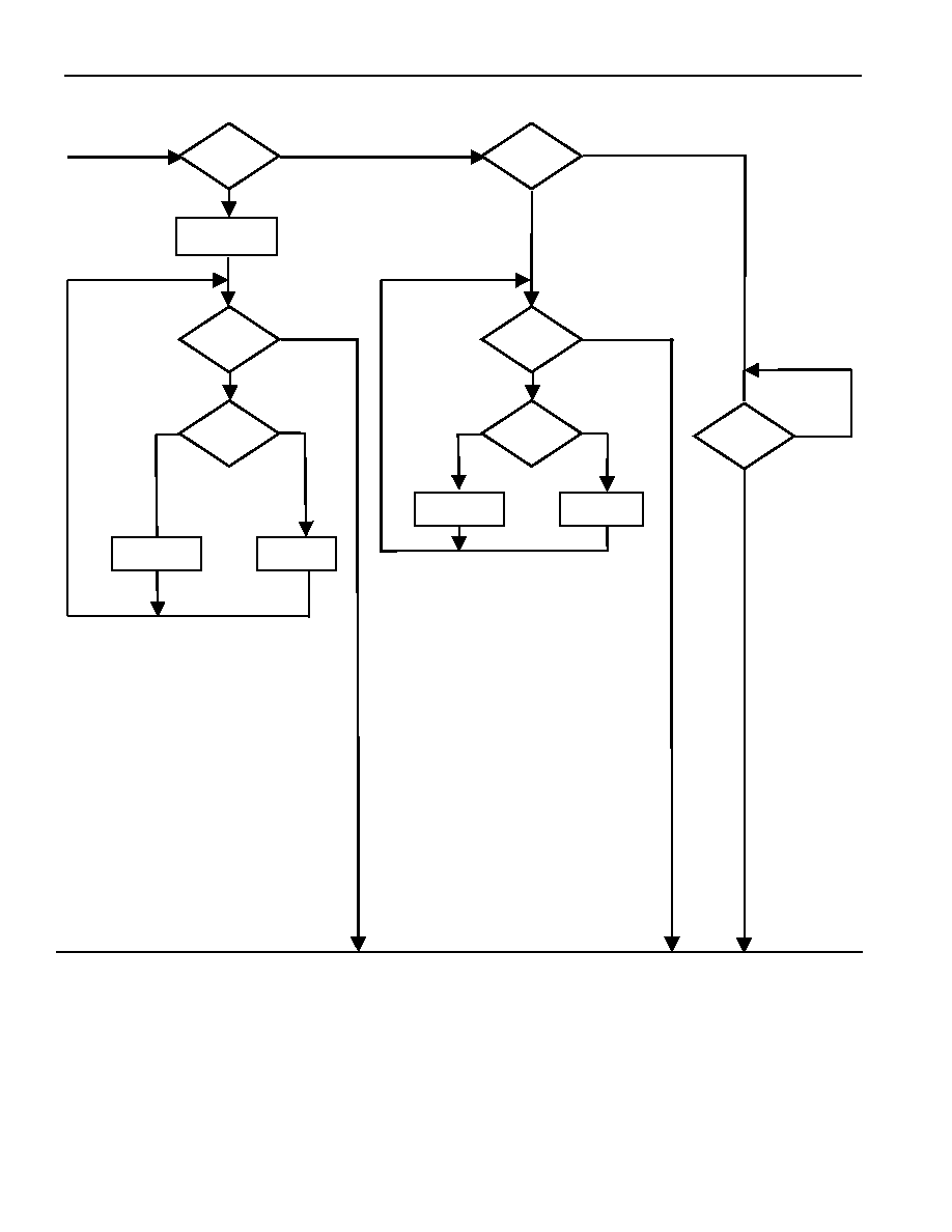
DS18S20
16 of 27
MEMORY FUNCTIONS FLOW CHART Figure 9 (cont'd)
N
MASTER T
X
RESET
?
DEVICE
BUSY CONVERTING
TEMPERATURE
?
N
Y
MASTER
RX "1"S
MASTER
R
X
"0"S
Y
DS18S20 RECALLS
FROM E
2
PROM
B8h
RECALL
E
2
?
Y
N
N
MASTER T
X
RESET
?
PARASITE
POWERED
?
N
Y
MASTER
RX "1"S
MASTER
R
X
"0"S
Y
B4h
READ
POWERSUPPLY
?
Y
N
MASTER
T
X
RESET
?
Y
N
DS18S20
17 of 27
INITIALIZATION PROCEDURE "RESET AND PRESENCE PULSES" Figure 10
DS18S20 COMMAND SET Table 2
INSTRUCTION
DESCRIPTION
PROTOCOL
1-WIRE BUS
AFTER ISSUING
PROTOCOL
NOTES
TEMPERATURE CONVERSION COMMANDS
Convert T
Initiates temperature
conversion.
44h
<read temperature busy
status>
1
MEMORY COMMANDS
Read Scratchpad
Reads bytes from
scratchpad and reads
CRC byte.
BEh
<read data up to 9 bytes>
Write Scratchpad
Writes bytes into
scratchpad at addresses 2
and 3 (TH and TL
temperature triggers).
4Eh
<write data into 2 bytes
at addr. 2 and addr 3>
Copy Scratchpad
Copies scratchpad into
nonvolatile memory
(addresses 2 and 3 only).
48h
<read copy status>
2
Recall E
2
Recalls values stored in
nonvolatile memory into
scratchpad (temperature
triggers).
B8h
<read temperature busy
status>
Read Power Supply Signals the mode of
DS18S20 power supply
to the master.
B4h
<read supply status>
LINE TYPE LEGEND
Bus master active low
DS18S20 active low
Both bus master and
Resistor pull-up
DS18S20 active low
Master T
X
"reset pulse"
480
µ
µ
µ
µ
s minmum
960
µ
µ
µ
µ
s maximum
Master R
X
480
µ
µ
µ
µ
s minmum
DS18S20 TX
waits
15-60
µ
µ
µ
µ
s
DS18S20 TX
"presence Pulse"
60-240
µ
µ
µ
µ
s
V
CC
GND
1-WIRE
BUS

DS18S20
18 of 27
NOTES:
1.
Temperature conversion takes up to 750 ms. After receiving the Convert T protocol, if the part does
not receive power from the V
DD
pin, the DQ line for the DS18S20 must be held high for at least
750 ms to provide power during the conversion process. As such, no other activity may take place on
the 1Wire bus for at least this period after a Convert T command has been issued.
2.
After receiving the Copy Scratchpad protocol, if the part does not receive power from the V
DD
pin, the
DQ line for the DS18S20 must be held high for at least 10 ms to provide power during the copy
process. As such, no other activity may take place on the 1Wire bus for at least this period after a
Copy Scratchpad command has been issued.
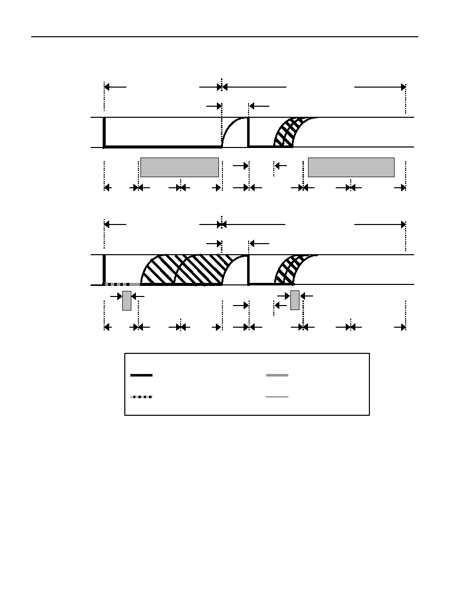
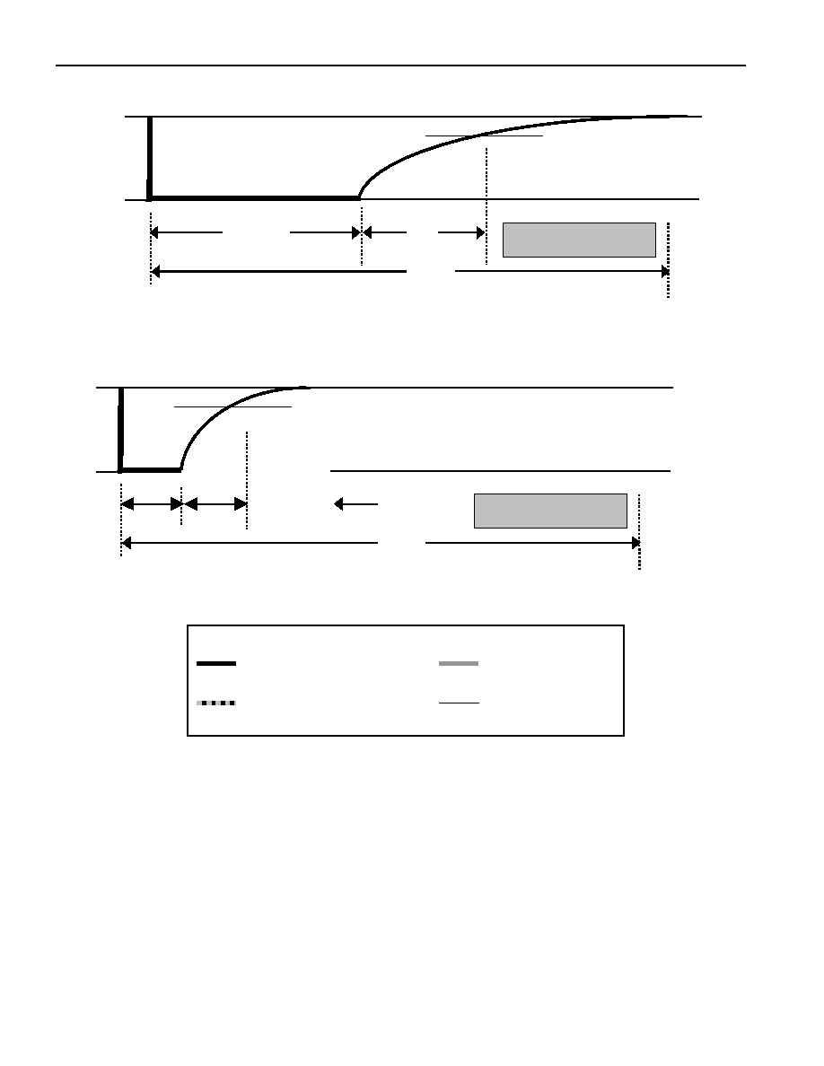
READ/WRITE TIME SLOTS
DS18S20 data is read and written through the use of time slots to manipulate bits and a command word to
specify the transaction.
Write Time Slots
A write time slot is initiated when the host pulls the data line from a high logic level to a low logic level.
There are two types of write time slots: Write 1 time slots and Write 0 time slots. All write time slots
must be a minimum of 60
µ
s in duration with a minimum of a 1-
µ
s recovery time between individual
write cycles.
The DS18S20 samples the DQ line in a window of 15
µ
s to 60
µ
s after the DQ line falls. If the line is
high, a Write 1 occurs. If the line is low, a Write 0 occurs (see Figure 11).
For the host to generate a Write 1 time slot, the data line must be pulled to a logic low level and then
released, allowing the data line to pull up to a high level within 15
µ
s after the start of the write time slot.
For the host to generate a Write 0 time slot, the data line must be pulled to a logic low level and remain
low for 60
µ
s.
Read Time Slots
The host generates read time slots when data is to be read from the DS18S20. A read time slot is initiated
when the host pulls the data line from a logic high level to logic low level. The data line must remain at a
low logic level for a minimum of 1
µ
s; output data from the DS18S20 is valid for 15
µ
s after the falling
edge of the read time slot. The host therefore must stop driving the DQ pin low in order to read its state
15
µ
s from the start of the read slot (see Figure 11). By the end of the read time slot, the DQ pin will pull
back high via the external pullup resistor. All read time slots must be a minimum of 60
µ
s in duration
with a minimum of a 1-
µ
s recovery time between individual read slots.
Figure 12 shows that the sum of T
INIT
, T
RC
, and T
SAMPLE
must be less than 15
µ
s. Figure 13 shows that
system timing margin is maximized by keeping T
INIT
and T
RC
as small as possible and by locating the
master sample time towards the end of the 15-
µ
s period.
DS18S20
19 of 27
READ/WRITE TIMING DIAGRAM Figure 11
Master Write
"0" Slot
60
µ
µ
µ
µ
s <T
x
"0" < 120
µ
µ
µ
µ
s
1
µ
µ
µ
µ
s < t
REC
<
V
CC
GND
1-WIRE
BUS
Master Write
"1" Slot
DS18S20 SAMPLES
MIN TYP MAX
>1
µ
µ
µ
µ
s
30
µ
µ
µ
µ
s
15
µ
µ
µ
µ
s
15
µ
µ
µ
µ
s
DS18S20 SAMPLES
MIN TYP MAX
15
µ
µ
µ
µ
s
15
µ
µ
µ
µ
s
30
µ
µ
µ
µ
s
Master Read
"0" Slot
1
µ
µ
µ
µ
s < t
REC
<
V
CC
GND
1-WIRE
BUS
Master Read
"1" Slot
>1
µ
µ
µ
µ
s
30
µ
µ
µ
µ
s
15
µ
µ
µ
µ
s
15
µ
µ
µ
µ
s
15
µ
µ
µ
µ
s
30
µ
µ
µ
µ
s
LINE TYPE LEGEND
Bus master active low
DS18S20 active low
Both bus master and
Resistor pull-up
DS18S20 active low
Master Samples
Master Samples
DS18S20
20 of 27
DETAILED MASTER READ 1 TIMING Figure 12
RECOMMENDED MASTER READ 1 TIMING Figure 13
T
INIT
>
>
>
>
1
µ
µ
µ
µ
s
V
CC
GND
1-WIRE
BUS
V
IH
OF MASTER
MASTER SAMPLES
T
RC
15
µ
µ
µ
µ
s
LINE TYPE LEGEND
Bus master active low
DS18S20 active low
Both bus master and
Resistor pull-up
DS18S20 active low
T
INIT
=
SMALL
V
CC
GND
1-WIRE
BUS
V
IH
OF MASTER
MASTER SAMPLES
15
µ
µ
µ
µ
s
T
RC
=
SMALL

DS18S20
21 of 27
Related Application Notes
The following Application Notes can be applied to the DS18S20. These notes can be obtained from the
Dallas Semiconductor "Application Note Book," via our website at
http://www.dalsemi.com/
.
Application Note 27: "Understanding and Using Cyclic Redundancy Checks with Dallas Semiconductor
Touch Memory Product"
Application Note 55: "Extending the Contact Range of Touch Memories"
Application Note 74: "Reading and Writing Touch Memories via Serial Interfaces"
Application Note 104: "Minimalist Temperature Control Demo"
Application Note 105: "High Resolution Temperature Measurement with Dallas DirecttoDirect
Temperature Sensors"
Application Note 106: "Complex MicroLANs"
Application Note 108: "MicroLAN In the Long Run"
Sample 1Wire subroutines that can be used in conjunction with AN74 can be downloaded from the
website or our Anonymous FTP Site.
MEMORY FUNCTION EXAMPLE Table 3
Example: Bus Master initiates temperature conversion, then reads temperature (parasite power assumed).
MASTER MODE
DATA (LSB FIRST)
COMMENTS
TX
Reset
Reset pulse (480-960 µs).
RX
Presence
Presence pulse.
TX
55h
Issue "Match ROM" command.
TX
<64-bit ROM code>
Issue address for DS18S20.
TX
44h
Issue " Convert T" command.
TX
<I/O LINE HIGH>
I/O line is held high for at least 750 ms by bus master to
allow conversion to complete.
TX
Reset
Reset pulse.
RX
Presence
Presence pulse.
TX
55h
Issue "Match ROM" command.
TX
<64-bit ROM code>
Issue address for DS18S20.
TX
BEh
Issue "Read Scratchpad" command.
RX
<9 data bytes>
Read entire scratchpad plus CRC; the master now
recalculates the CRC of the eight data bytes received
from the scratchpad, compares the CRC calculated and
the CRC read. If they match, the master continues; if
not, this read operation is repeated.
TX
Reset
Reset pulse.
RX
Presence
Presence pulse, done.

DS18S20
22 of 27
MEMORY FUNCTION EXAMPLE Table 4
Example: Bus Master writes memory (parasite power and only one DS18S20 assumed).
MASTER MODE
DATA (LSB FIRST)
COMMENTS
TX
Reset
Reset pulse.
RX
Presence
Presence pulse.
TX
CCh
Skip ROM command.
TX
4Eh
Write Scratchpad command.
TX
<2 data bytes>
Writes 2 bytes to scratchpad (TH and TL).
TX
Reset
Reset pulse.
RX
Presence
Presence pulse.
TX
CCh
Skip ROM command.
TX
BEh
Read Scratchpad command.
RX
<9 data bytes>
Read entire scratchpad plus CRC. The master now
recalculates the CRC of the eight data bytes received
from the scratchpad, compares the CRC and the two
other bytes read back from the scratchpad. If data match,
the master continues; if not, repeat the sequence.
TX
Reset
Reset pulse.
RX
Presence
Presence pulse.
TX
CCh
Skip ROM command.
TX
48h
Copy Scratchpad command; after issuing this command,
the master must wait 10 ms for copy operation to
complete.
TX
Reset
Reset pulse.
RX
Presence
Presence pulse, done.

DS18S20
23 of 27
MEMORY FUNCTION EXAMPLE Table 5
Example: Temperature conversion and interpolation (external power supply and only one DS18S20
assumed.)
MASTER MODE
DATA (LSB FIRST)
COMMENTS
TX
Reset
Reset pulse.
TR
Presence
Presence pulse.
TX
CCh
Skip ROM command.
TX
44h
Convert T command.
RX
<1 data byte>
Read busy flag eight times. The master continues
reading 1 byte (or bit) after another until the data is FFh
(all bits 1).
TX
Reset
Reset pulse.
RX
Presence
Presence pulse.
TX
CCh
Skip ROM command.
TX
BEh
Read Scratchpad command.
RX
<9 data bytes>
Read entire scratchpad plus CRC. The master now
recalculates the CRC of the eight data bytes received
from the scratchpad and compares both CRCs. If the
CRCs match, the data is valid. The master saves the
temperature value and stores the contents of the count
register and count per °C register as COUNT_REMAIN
and COUNT_PER_C, respectively.
TX
Reset
Reset pulse.
RX
Presence
Presence pulse, done.
-
-
CPU calculates temperature as described in the data
sheet for higher resolution.

DS18S20
24 of 27
ABSOLUTE MAXIMUM RATINGS*
Voltage on Any Pin Relative to Ground
0.5V to +6.0V
Operating Temperature
55
°
C to +125
°
C
Storage Temperature
55
°
C to +125
°
C
Soldering Temperature
See J-STD-020A specification
* This is a stress rating only and functional operation of the device at these or any other conditions above
those indicated in the operation sections of this specification is not implied. Exposure to absolute
maximum rating conditions for extended periods of time may affect reliability.
RECOMMENDED DC OPERATING CONDITIONS
PARAMETER
SYMBOL
CONDITION
MIN
TYP
MAX
UNITS NOTES
Supply Voltage
V
DD
Local Power
3.0
5.5
V
1
Data Pin
DQ
-0.3
V
DD
V
1
Logic 1
V
IH
2.2
V
DD
+0.3
V
1,2
Logic 0
V
IL
-0.3
+0.8
V
1,3,7
DC ELECTRICAL CHARACTERISTICS
(-55°C to +125°C; V
DD
=3.0V to 5.5V)
PARAMETER
SYMBOL
CONDITION
MIN
TYP
MAX
UNITS
NOTES
Thermometer Error
t
ERR
-10°C to +85°C
±˝
°C
-55°C to +125°C
±2
Input Logic High
V
IH
Local Power
Parasite Power
2.2
3.0
5.5
V
V
1,2
1,2
Input Logic Low
V
IL
-0.3
+0.8
V
1,3, 7
Sink Current
I
L
V
I/O
=0.4V
-4.0
mA
1
Standby Current
I
DDS
750
1000
nA
6,8
Active Current
I
DD
1
1.5
mA
4
DQ Input Load
Current
I
DQ
5
µA
5
AC ELECTRICAL CHARACTERISTICS: NV MEMORY
(-55°C to +125°C; V
DD
=3.0V to 5.5V)
PARAMETER
SYMBOL
CONDITION
MIN
TYP
MAX
UNITS NOTES
NV Write Cycle Time
t
WR
2
10
ms
EEPROM Writes
N
EEWR
-55°C to +55°C
50k
writes
EEPROM Data
Retention
t
EEDR
-55°C to +55°C
10
years

DS18S20
25 of 27
AC ELECTRICAL CHARACTERISTICS:
(-55°C to +125°C; V
DD
=3.0V to 5.5V)
PARAMETER
SYMBOL CONDITION
MIN
TYP
MAX
UNITS NOTES
Temperature Conversion
t
CONV
200
750
ms
Time
Time Slot
t
SLOT
60
120
µs
Recovery Time
t
REC
1
µs
Write 0 Low Time
r
LOW0
60
120
µs
Write 1 Low Time
t
LOW1
1
15
µs
Read Data Valid
t
RDV
15
µs
Reset Time High
t
RSTH
480
µs
Reset Time Low
t
RSTL
480
µs
9
Presence Detect High
t
PDHIGH
15
60
µs
Presence Detect Low
t
PDLOW
60
240
µs
Capacitance
C
IN/OUT
25
pF
NOTES:
1.
All voltages are referenced to ground.
2.
Logic one voltages are specified at a source current of 1 mA.
3.
Logic zero voltages are specified at a sink current of 4 mA.
4.
Active current refers to either temperature conversion or writing to the E
2
memory. Writing to E
2
memory consumes approximately 200
µ
A for up to 10 ms.
5.
Input load is to ground.
6.
Standby current specified up to 70
°
C. Standby current typically is 3
µ
A at 125
°
C.
7.
To always guarantee a presence pulse under low voltage parasite power conditions, V
ILMAX
may have
to be reduced to as much as 0.5V.
8.
To minimize I
DDS
, DQ should be GND
DQ
GND + 0.3V or V
DD
0.3V
DQ
V
DD
.
9.
Under parasite power, the max t
RSTL
before a power on reset occurs, is 960 ms.
DS18S20
26 of 27
1--WIRE WRITE ONE TIME SLOT
1--WIRE WRITE ZERO TIME SLOT
1--WIRE READ ZERO TIME SLOT
1--WIRE RESET PULSE
1-WIRE PRESENCE DETEST
DS18S20
27 of 27
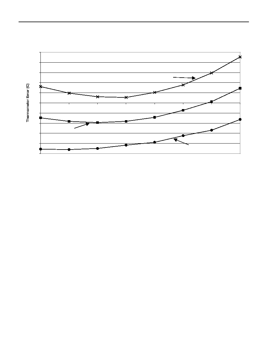
TYPICAL PERFORMANCE CURVE
DS18S20 Typical Error Curve
-0.5
-0.4
-0.3
-0.2
-0.1
0
0.1
0.2
0.3
0.4
0.5
0
10
20
30
40
50
60
70
Reference Temp (C)
Mean Error
+3
Error
-3
Error