
1 of 9
020702
FEATURES
Ï 5V or 3.3V power-on reset
Ï True 3V operation power switch
Ï Switches to battery at 3.8V (2.6V for 3.3V
versions)
Ï Excellent for systems designed to operate
with dual power supplies
Ï Asserts resets during power transients
Ï Maintains reset for 350ms after V
CC
returns to
an in-tolerance condition
Ï Reduces need for discrete components
Ï Precision temperature-compensated voltage
reference and voltage sensor
Ï 8-pin DIP or space saving 8-pin SO surface
mount available
Ï CMOS reset output for low current operation
Ï Operating temperature of -40¯C to +85¯C
Ï Perfect for PIC microprocessor applications
PIN ASSIGNMENT
DS1836A/C (*DS1836B/D)
PIN DESCRIPTION
V
CC
- Power Supply Input
V
BAT
- Battery Supply Input
NC
- No Connect
V
OUT
- Power Supply Output
GND -
Ground
IN -
Sense
Input
NMI
-
Non-maskable
Interrupt
RST
(*RST)
- Reset Output
DESCRIPTION
The DS1836 MicroManager performs three vital system functions. First, a precision temperature-
compensated reference and comparator circuit monitor the status of the voltage on V
CC
and when an out-
of-tolerance condition is detected, an internal power-fail signal is generated that forces the reset active. If
V
CC
continues to degrade, it switches to the battery supply when V
CC
drops below 3.8V (2.6V for 3.3V
versions). When V
CC
exceeds 3.9V (2.8V for 3.3V versions); V
OUT
will again be supplied from V
CC
.
Reset will remain active for 350 ms after V
CC
returns to an in-tolerance condition.
Lastly, the DS1836 supports a sense input that sends a non-maskable interrupt whenever the sense input
drops below 1.25V.
DS1836/A/B/C/D
3.3V/5V MicroManager
www.maxim-ic.com
8-Pin SO (150mil)
1
2
3
4
8
7
6
5
V
CC
V
BAT
NC
V
OUT
RST(*RST)
NMI
IN
GND
8-Pin DIP (300mil)
V
CC
V
BAT
NC
V
OUT
RST(*RST)
NMI
IN
GND
1
2
3
4
8
7
6
5
DS1836A/B/C/D
2 of 9
OPERATION
Power Monitor
The DS1836 provides the functions of detecting out-of-tolerance conditions on a 3.3V or 5V power
supply and warning a processor-based system of impending power failure. When V
CC
is detected as out of
tolerance the RST will be forced active. When V
CC
returns to a valid state the RST will remain active for
about 350ms and then return to an inactive state until the next V
CC
out-of-tolerance condition.
On power-up reset is kept active for approximately 350ms after the power supply input has reached the
selected tolerance. This allows the power supply and system power to stabilize before RST is released.
Power Switch (DS1836A & B)
The DS1836 switches the V
OUT
output between V
CC
and V
BAT
. On the initial power-up, V
OUT
draws
current from the V
BAT
input until V
CC
exceeds 3.9V. When V
CC
exceeds 3.9V V
OUT
switches from V
BAT
to V
CC
and will not switch back to V
BAT
until V
CC
drops below 3.8V. When V
CC
is below 3.8V, power
will be drawn from the supply with the highest voltage: either V
CC
or V
BAT
.
Power Switch (DS1836C & D)
The DS1836 switches the V
OUT
output between V
CC
and V
BAT
. On the initial power up, V
OUT
draws
current from the V
BAT
input until V
CC
exceeds 2.8V. When V
CC
exceeds 2.8V V
OUT
switches from V
BAT
to V
CC
and will not switch back to V
BAT
until V
CC
drops below 2.6V. When V
CC
is below 2.6V, power
will be drawn from the supply with the highest voltage either V
CC
or V
BAT
.
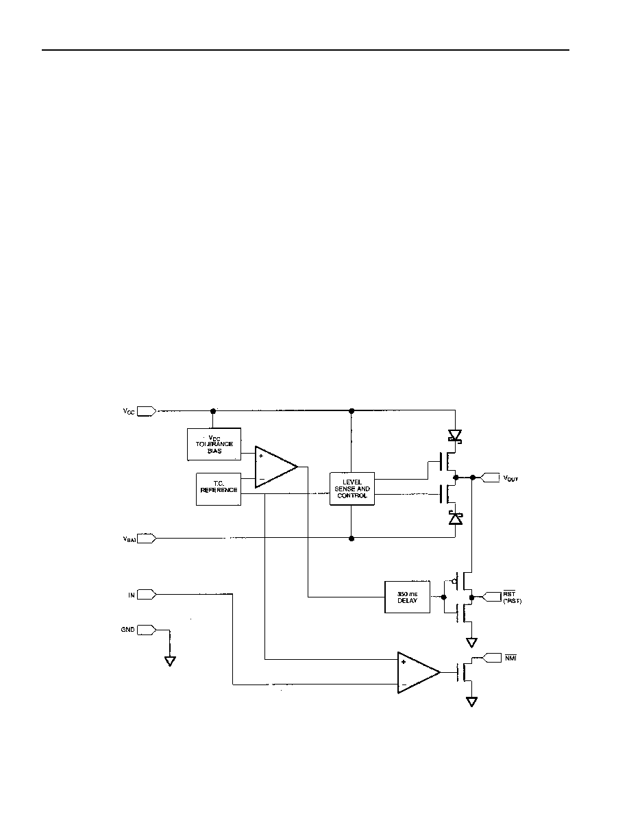
BLOCK DIAGRAM Figure 1
* DS1836B and DS1836D
DS1836A/B/C/D
3 of 9
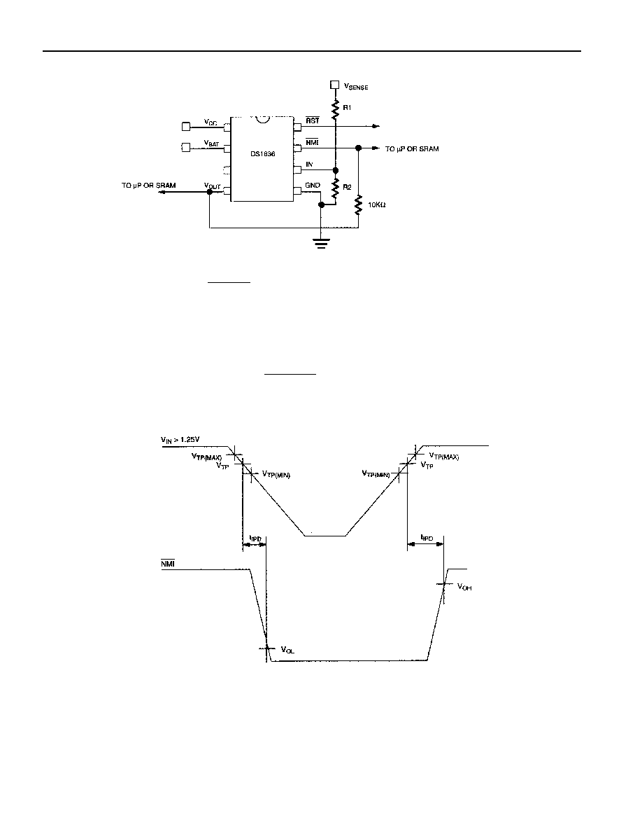
Non-Maskable Interrupt
The DS1836 generates a non-maskable interrupt (
NMI
) for early warning of a power failure. A precision
comparator monitors the voltage level at the IN pin relative to an on-chip reference generated by an
internal band gap. The IN pin is a high impedance input allowing for a user-defined sense point. An
external resistor voltage divider network (Figure 3) is used to interface with high voltage signals. This
sense point may be derived from a regulated supply or from a higher DC voltage level closer to the main
system power input. Since the IN trip point V
TP
is 1.25V, the proper values for R1 and R2 can be
determined by the equation as shown in Figure 3. Proper operation of the DS1836 requires that the
maximum voltage at the IN pin be limited to the active supply (V
CC
or V
BAT
). Therefore, the maximum
allowable voltage at the supply being monitored (V
MAX
) can also be derived as shown in Figure 3. A
simple approach to solving the equation is to select a value for R2 high enough to keep power
consumption low and solve for R1. The flexibility of the IN input pin allows for detection of power loss
at the earliest point in a power supply system, maximizing the amount of time for system shutdown
between
NMI
and RST (or
RST
).
A pull-up resistor is required for proper operation of the
NMI
open-drain output. A 10k
W resistor would
be a typical value for the pull-up resistor.
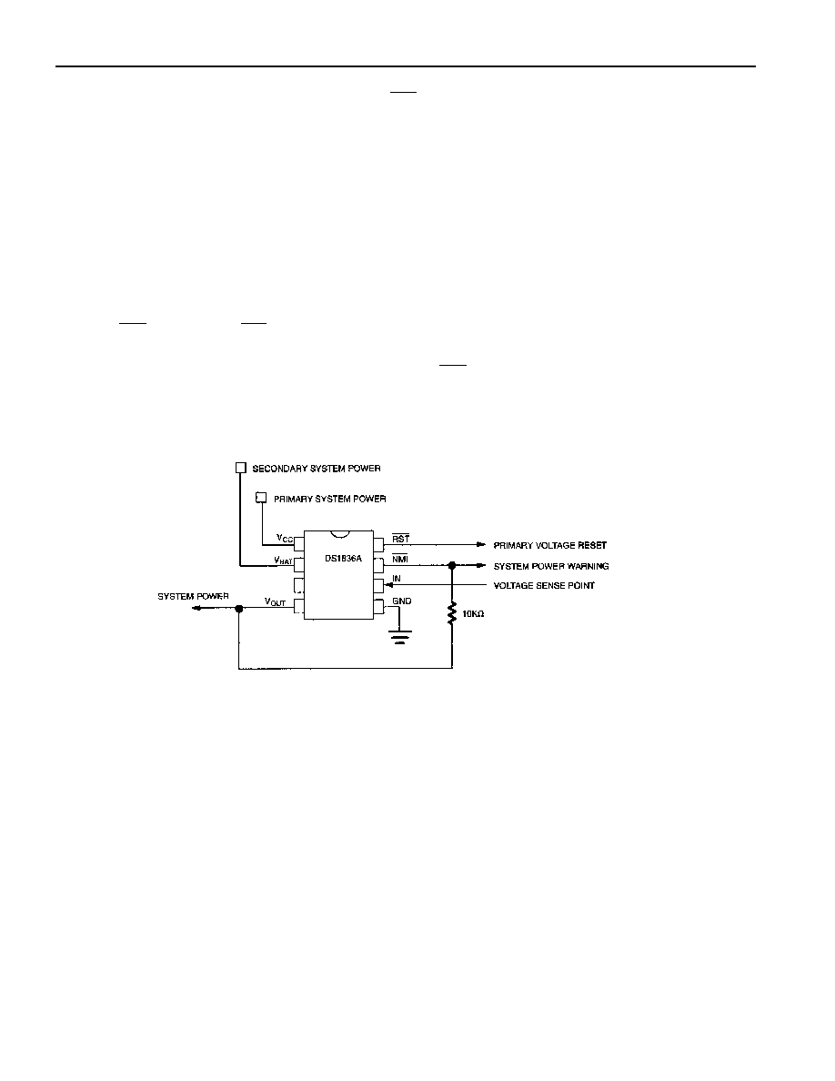
TYPICAL APPLICATION
Figure 2
DS1836A/B/C/D
4 of 9
NON-MASKABLE INTERRUPT CIRCUIT EXAMPLE Figure 3
V
SENSE
=
R2
R2
R1
+
x 1.25
Example:
V
SENSE
= 4.50V at the trip point
100k
W = R2
Therefore:
4.5 =
100k
100k
R1
+
x 1.25
R1 = 260k
W
TIMING DIAGRAM: NON-MASKABLE INTERRUPT Figure 4
DS1836A/B/C/D
5 of 9
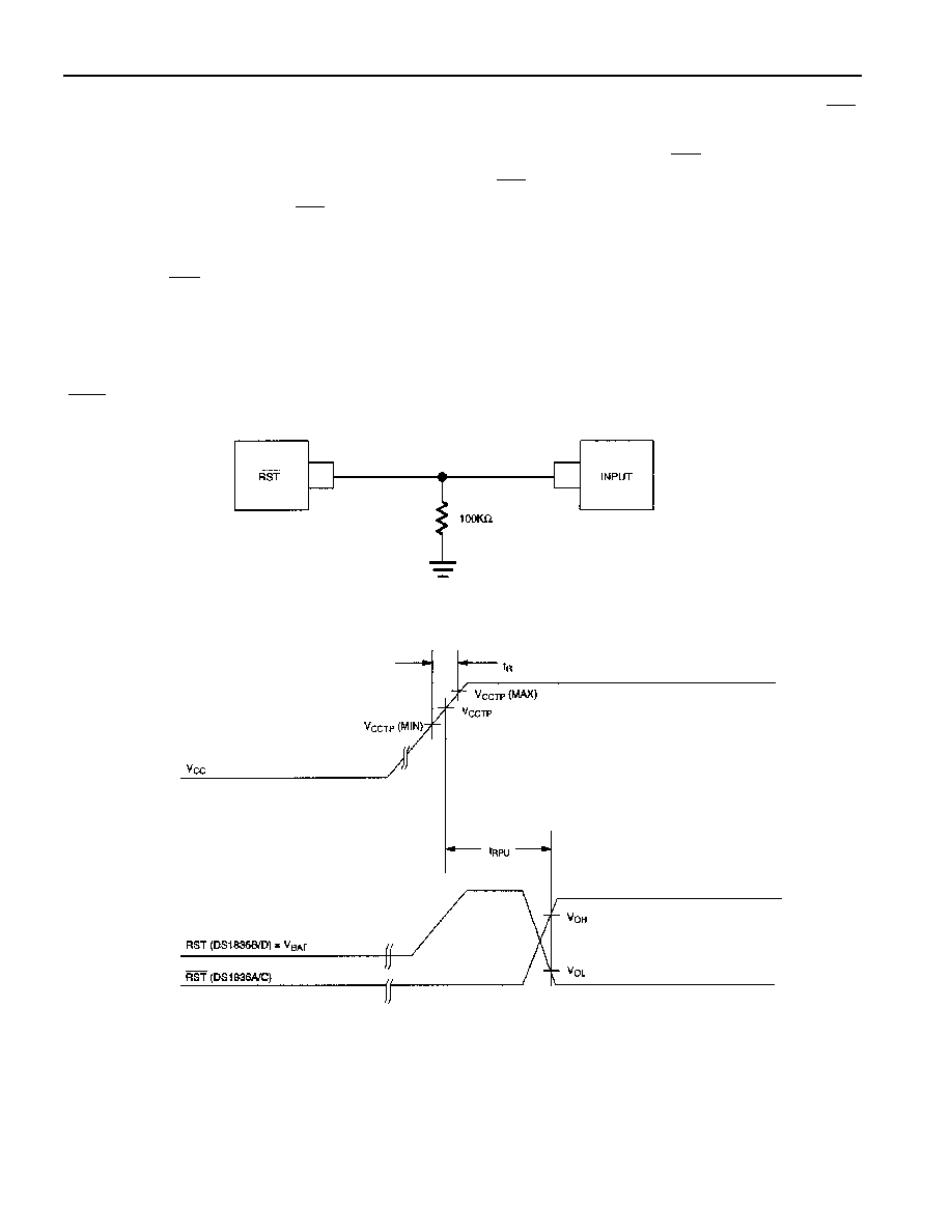
OUTPUT VALID CONDITIONS
The DS1836 can maintain valid outputs as long as one input remains above 1.2V. However, the
RST
outputs on the DS1836A (or C) use a push-pull output structure which can maintain a valid output below
1.2V on an input. To sink current below 1.2V a resistor can be connected from
RST
to GND (see Figure
5). This arrangement will maintain a valid value on the
RST
outputs even if all supply inputs are at 0V.
During conditions when the
RST
is in the inactive or high state this arrangement will draw current
through the pull down resistor. A value of about 100 k
W should be adequate to maintain a valid condition.
The DS1836
NMI
output requires a pull-up resistor on the output to maintain a valid output. The value of
the resistor is not critical in most cases but must be set low enough to pull the output to a high state. A
common value used is 10k
Ws (see Figure 3).
APPLICATION DIAGRAM:
RST
VALID TO 0V V
CC
ON THE DS1836A OR DS1836C
Figure 5
TIMING DIAGRAM: POWER-UP Figure 6