1 of 8
122001
FEATURES
§ Halts and restarts an out-of-control
microprocessor
§ Holds microprocessor in check during power
transients
§ Automatically restarts microprocessor after
power failure
§ Monitors pushbutton for external override
§ Accurate 5%, 10%, or 20% (3V only)
microprocessor power monitoring
§ Eliminates the need for discrete components
§ 20% tolerance for use with 3.0V systems
§ Pin- and function-compatible with the
MAX823/24/25 products
§ Low cost SOT-23-5 package
§ Industrial temperature range: -40°C to +85°C
DEVICE
RST
RST
PBRST
WD
DS181xA
DS181xB
DS181xC
X
X
X
X
X
X
X
X
X
x = "DS1814" for 5V devices
x = "DS1819" for 3V devices
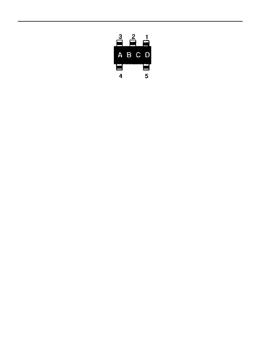
PIN ASSIGNMENT
PIN DESCRIPTION
DS181xA
1
RST
Active Low Reset Output
2
GND
Ground
3
PBRST
Pushbutton Reset Input
4
ST
Strobe Input
5
VCC
Power Supply
DS181xB
1
RST
Active Low Reset Output
2
GND
Ground
3
RST
Active High Reset Output
4
ST
Strobe Input
5
VCC
Power Supply
DS181xC
1
RST
Active Low Reset Output
2
GND
Ground
3
RST
Active High Reset Output
4
PBRST
Pushbutton Reset Input
5 VCC
Power
Supply
DESCRIPTION
The DS1814 5-Volt MicroMonitor and the DS1819 3.3V MicroMonitor monitor three vital conditions for
a microprocessor: power supply, software execution, and external override. First, a precision temperature-
compensated reference and comparator circuit monitor the status of V
CC
. When an out-of-tolerance
condition occurs, an internal power-fail signal is generated which forces the reset(s) to an active state.
When V
CC
returns to an in-tolerance condition, the reset signal is kept in the active state for a minimum of
140ms to allow the power supply and processor to stabilize.
DS1814/DS1819
5V and 3.3V MicroMonitor
www.maxim-ic.com
3
2
1
4
5
SOT-23-5 PACKAGE
See Mech. Drawing

DS1814/DS1819
2 of 8
The DS1814/DS1819 `A' and `C' perform pushbutton reset control. They debounce the pushbutton input
and generate an active reset pulse width of 140ms minimum. The DS1814/9 `A' and `B' versions perform
a watchdog function. The watchdog is an internal timer that forces the reset signals to the active state if
the strobe input does not change state every 1.12 seconds. The watchdog timer function can be disabled
by leaving the watchdog strobe input disconnected.
OPERATION
Power Monitor
The DS1814 detects out-of-tolerance power supply conditions and warns a processor-based system of
impending power failure. When V
CC
falls below a preset level, a comparator outputs the signal
RST
(or
RST).
RST
(or RST) are excellent control signals for a microprocessor, as processing is stopped at the
last possible moment of valid V
CC
. On power-up,
RST
(or RST) are kept active for a minimum of 140ms
to allow the power supply and processor to stabilize.
Pushbutton Reset
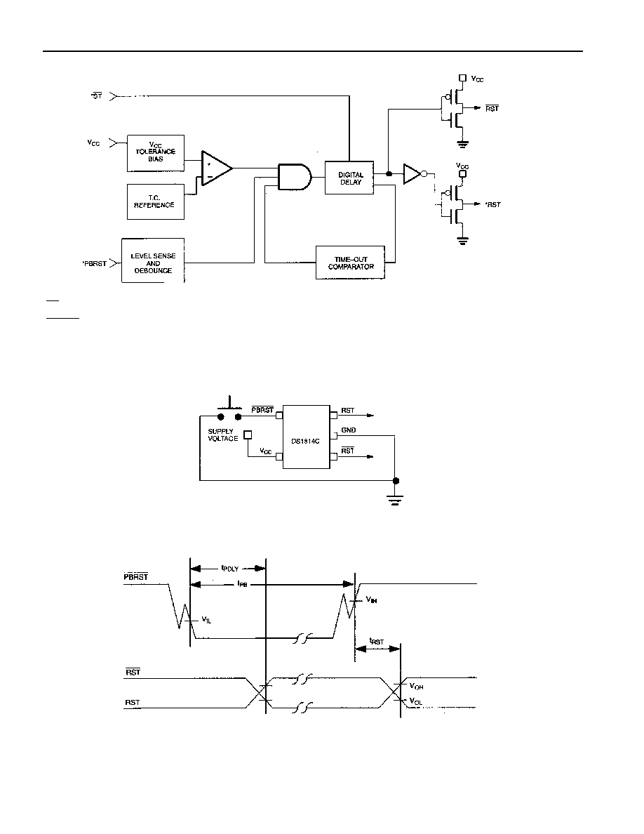
The DS1814 `A' and `C' provide an input pin for direct connection to a pushbutton reset (see Figure 2).
The pushbutton reset input requires an active low signal. Internally, this input is debounced and timed
such that a
RST
(or RST) signal of at least 140ms minimum will be generated. The 140ms delay
commences as the pushbutton reset input is released from the low level (see Figure 3).
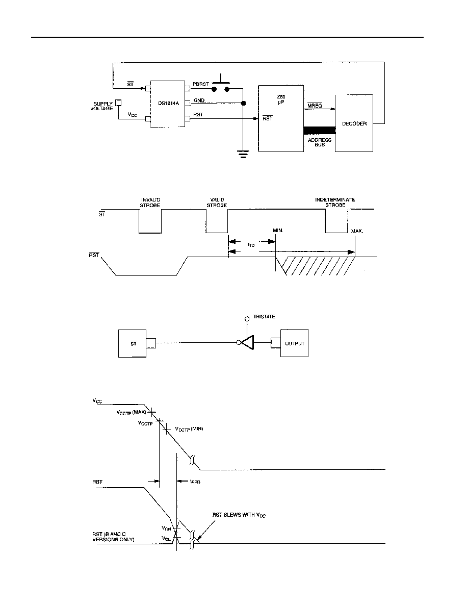
Watchdog Timer
The DS1814/DS1819 `A' and `B' versions watchdog timer function forces
RST
(and RST) signal(s)
active when the
ST
input is not clocked within the 1.12 second watchdog time-out period. Time-out of
the watchdog starts when
RST
(and RST) become(s) inactive. If a transition occurs on the
ST
input pin
prior to time-out, the watchdog timer is reset and begins to time out again. If the watchdog timer is
allowed to time out, then the reset output(s) will go active for 140ms. The watchdog can be disabled by
floating (or tri-stating) the
ST
input.
The
ST
input can be derived from many microprocessor outputs. The most typical signals used are the
microprocessor data I/O signals and control signals. When the microprocessor functions normally, these
signals would as a matter of routine cause the watchdog to be reset prior to time-out. To guarantee that
the watchdog timer does not time out, a transition must occur at or less than 1.12 seconds. A typical
circuit example is shown in Figure 4. The DS1814/19 watchdog function can be disabled at any time by
tri-starting the strobe input. A sample circuit to disable the watchdog is shown in Figure 6.
DS1814/DS1819
3 of 8
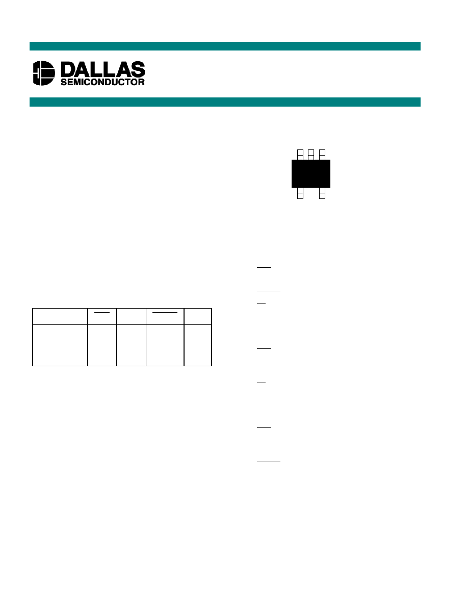
DS1814/DS1819 BLOCK DIAGRAM Figure 1
*Notes:
ST
available on'A' and 'B' versions
PBRST
available on 'A' and 'C' versions
RST available on 'B' and 'C' versions
PUSHBUTTON RESET Figure 2
TIMING DIAGRAM: PUSHBUTTON RESET Figure 3
DS1814/DS1819
4 of 8
WATCHDOG TIMER Figure 4
TIMING DIAGRAM: STROBE INPUT Figure 5
WATCHDOG DISABLE CIRCUIT Figure 6
TIMING DIAGRAM: POWER-DOWN Figure 7
DS1814/DS1819
5 of 8
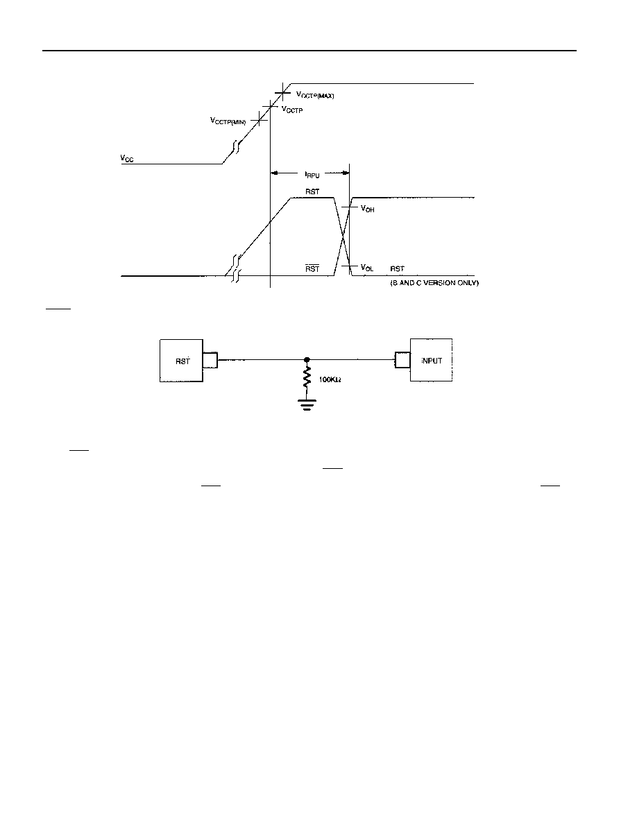
TIMING DIAGRAM: POWER-UP Figure 8
RST
VALID TO 0 VOLTS V
CC
Figure 9
OUTPUT VALID CONDITIONS
The
RST
output uses a push-pull output which can maintain a valid output down to 1.0V V
CC
. To sink
current below 1.0V a resistor can be connected form
RST
to Ground (see Figure 9.) This arrangement
will maintain a valid value on
RST
during both power-up and -down but will draw current when
RST
is
in the high state. A value of about 100k
W should be adequate in most situations. The output with a
resistor pull-down can maintain a valid reset down to V
CC
equal to 0V.

DS1814/DS1819
6 of 8
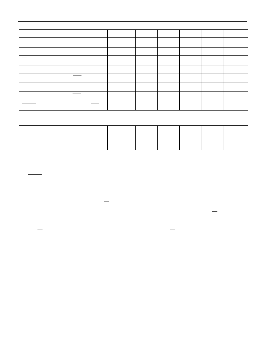
ABSOLUTE MAXIMUM RATINGS*
Voltage on V
CC
Pin Relative to Ground
-0.5V to +7.0V
Voltage on I/O Relative to Ground
-0.5V to V
CC
+ 0.5V
Operating Temperature Range
-40
°C to +85°C
Storage Temperature Range
-55
°C to +125°C
Soldering Temperature
260
°C for 10 seconds
* This is a stress rating only and functional operation of the device at these or any other conditions
above those indicated in the operation sections of this specification is not implied. Exposure to
absolute maximum rating conditions for extended periods of time may affect reliability.
RECOMMENDED DC OPERATING CONDITIONS
(-40
°
C to +85
°
C)
PARAMETER
SYMBOL
MIN
TYP
MAX
UNITS NOTES
Supply Voltage
V
CC
1.0
5.5
V
1
ST
and
PBRST
Input High Level
V
IH
0.8 V
CC
V
1
ST
and
PBRST
Input Low Level
V
IL
0.3 V
CC
V
1
DC ELECTRICAL CHARACTERISTICS (-40
°C to +85°C; V
CC
= 1.2V to 5.5V)
PARAMETER
SYMBOL
MIN
TYP
MAX
UNITS NOTES
V
CC
Trip Point DS1814-5
V
CCTP
4.50
4.75
V
1
V
CC
Trip Point DS1814-10
V
CCTP
4.25
4.50
V
1
V
CC
Trip Point DS1819-5
V
CCTP
3.00
3.15
V
1
V
CC
Trip Point DS1819-10
V
CCTP
2.85
3.00
V
1
V
CC
Trip Point DS1819-20
V
CCTP
2.55
2.70
V
1
Reset Trip Point Hysteresis (DS1814)
V
RH
10
mV
Reset Trip Point Hysteresis (DS1819)
V
RH
5
mV
Output Current @ 2.4V
I
OH
350
mA
3
Output Current @ 0.4V
I
OL
3.2
6
mA
3
Output Voltage @ -30
mA
V
OH
V
CC
*.8
V
CC
*.9
V
3
Operating Current DS1814
I
CC
10
15
mA
4
Operating Current DS1819
I
CC
8
12
mA
5
ST
Input Current
ST
= V
CC
, Time Averaged
120
160
mA
6
ST
Input Current
ST
= GND, Time Averaged
-20
-15
mA
6
DS1814/DS1819
7 of 8
AC ELECTRICAL CHARACTERISTICS (-40
°C to +85°C; V
CC
= 1.2V to 5.5V)
PARAMETER
SYMBOL
MIN
TYP
MAX
UNITS NOTES
PBRST
= V
IL
t
PB
1
ms
7
Reset Active Time
t
RST
140
200
280
ms
ST
Pulse Width
t
ST
50
ns
8
Watchdog Time-out
t
TD
1.12
1.60
2.40
s
V
CC
Detect to RST and
RST
t
RPD
30
40
ms
9
V
CC
Slew Rate (rising edge)
12.5
V/
ms
V
CC
Detect to RST and
RST
t
RPU
140
200
280
ms
PBRST
Stable Low to RST and
RST
t
PDLY
500
ns
CAPACITANCE
(t
A
= 25
°
C)
PARAMETER
SYMBOL
MIN
TYP
MAX
UNITS NOTES
Input Capacitance
C
IN
5
pF
Output Capacitance
C
OUT
7
pF
NOTES:
1) All voltages are referenced to ground.
2)
PBRST
is internally pulled up to V
CC
with an internal impedance of 50k
W typical.
3) Measured with V
CC
ł 2.7V.
4) Measured with outputs open, V
CC
Ł 5.5V, and all inputs at V
CC
or Ground, except the
ST
input at
<10kHz duty cycle-square wave or
ST
input open.
5) Measured with outputs open, V
CC
Ł 3.6V, and all inputs at V
CC
or Ground, except the
ST
input at
<10kHz duty cycle-square wave or
ST
input open.
6) The
ST
input current is defined as the average input current when
ST
is driven high or low. This input
must be driven high or low by an output that can source or sink at least 200
mA when active.
7) Noise immunity: pulses <100ns at pushbutton input will not cause a reset.
8) Must not exceed t
TD
minimum.
9) Noise immunity: pulses <2
ms at V
CCTP
minimum will not cause a reset and V
CCTP
- V
CC
= 100mV.
DS1814/DS1819
8 of 8
PART MARKING CODES
`A', `B' and `C' represents the Device Type.
14A - DS1814A
14B - DS1814B
14C - DS1814C
19A - DS1819A
19B - DS1819B
19C - DS1819C
`D' represents the Device Tolerance.
A -
5%
B -
10%
C -
20%
SOT-23-5 PACKAGE