
1 of 5
111999
FEATURES
Automatically restarts a microprocessor after
power failure
Maintains reset for 150 ms after V
CC
returns
to an in-tolerance condition
Reduces need for discrete components
Precision temperature-compensated voltage
reference and voltage sensor
Accurate 5%, 10% or 20% power monitoring
20% tolerance for use with 3.0-volt systems
Low-cost TO-92 or space saving surface
mount SOT-23 packages available
Push-pull active high output
Operating temperature -40°C to +85°C
PIN ASSIGNMENT
PIN DESCRIPTION
TO-92
1
RST
Active High Reset Output
2 V
CC
Power
Supply
3 GND Ground
SOT-23
1
RST
Active High Reset Output
2 V
CC
Power
Supply
3 GND Ground
DESCRIPTION
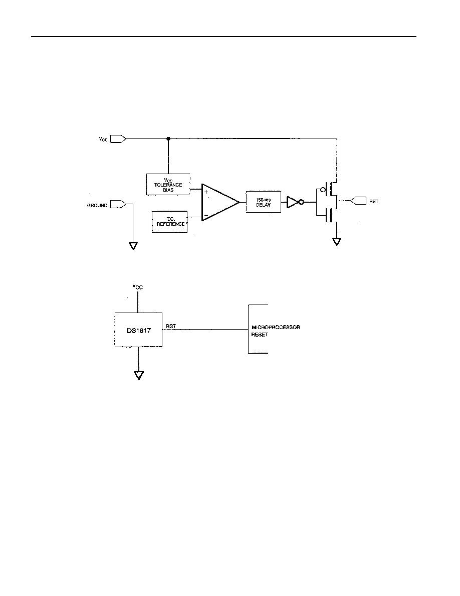
The DS1817 EconoReset uses a precision temperature reference and comparator circuit to monitor the
status of the power supply (V
CC
). When an out-of-tolerance condition is detected, an internal power-fail
signal is generated which forces reset to the active state. When V
CC
returns to an in-tolerance condition,
the reset signal is kept in the active state for approximately 150 ms to allow the power supply and
processor to stabilize.
DS1817
Active High 3.3V EconoReset
www.dalsemi.com
1
2
3
SOT-23 PACKAGE
See Mech. Drawing
1 2 3
1 2 3
TO-92 PACKAGE
See Mech. Drawing
DS1817
2 of 5
OPERATION - POWER MONITOR
The DS1817 provides the function of detecting out-of-tolerance power supply conditions and warning a
processor based system of impending power failure. When V
CC
is detected as out-of-tolerance, the RST
signal is asserted. On power-up, RST is kept active for approximately 150 ms after the power supply has
reached the selected tolerance. This allows the power supply and microprocessor to stabilize before RST
is released.
BLOCK DIAGRAM (CMOS OUTPUT) Figure 1
APPLICATION EXAMPLE Figure 2
DS1817
3 of 5
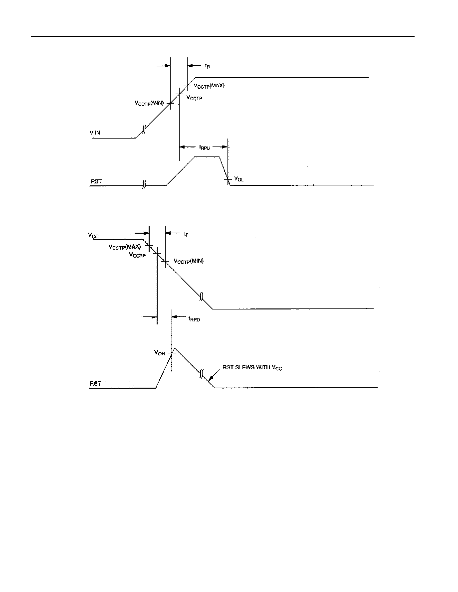
TIMING DIAGRAM: POWER-UP Figure 3
TIMING DIAGRAM: POWER-DOWN Figure 4

DS1817
4 of 5
ABSOLUTE MAXIMUM RATINGS*
Voltage on V
CC
Pin Relative to Ground
-0.5V to +7.0V
Voltage on RST Relative to Ground
-0.5V to 5V
CC
+0.5V
Operating Temperature
-40°C to +85°C
Storage Temperature
-55°C to +125°C
Soldering Temperature
260°C for 10 seconds
*
This is a stress rating only and functional operation of the device at these or any other conditions
above those indicated in the operation sections of this specification is not implied. Exposure to
absolute maximum rating conditions for extended periods of time may affect reliability.
RECOMMENDED DC OPERATING CONDITIONS (-40
°
C to +85
°
C)
PARAMETER
SYMBOL
MIN
TYP
MAX
UNITS NOTES
Supply Voltage
V
CC
0.0
5.5
V
1
DC ELECTRICAL CHARACTERISTICS (-40
°
C to +85
°
C; V
CC
=1.2V to 5.5V)
PARAMETER
SYMBOL
MIN
TYP
MAX
UNITS NOTES
Output Voltage @ 0-500
µ
A
V
OH
V
CC
-0.5V
V
CC
-0.1V
V
1
Output Current @ 2.4V
I
OH
350
µ
A
2
Output Current @ 0.4V
I
OL
+10
mA
2
Operating Current V
CC
< 5.5
I
CC
28
35
µ
A
3
V
CC
Trip Point (DS1817-5)
V
CCTP
2.98
3.06
3.15
V
1
V
CC
Trip Point (DS1817-10)
V
CCTP
2.80
2.88
2.97
V
1
V
CC
Trip Point (DS1817-20)
V
CCTP
2.47
2.55
2.64
V
1
Output Capacitance
C
OUT
10
pF
AC ELECTRICAL CHARACTERISTICS (-40
°
C to +85
°
C; V
CC
=1.2V to 5.5V)
PARAMETER
SYMBOL
MIN
TYP
MAX
UNITS NOTES
RESET Active Time
t
RST
100
150
250
ms
V
CC
Detect to RST
t
RPD
2
5
µ
s
V
CC
Slew Rate
(V
CCTP
(MAX) to V
CCTP
(MIN))
t
F
300
µ
s
6
V
CC
Slew Rate
(V
CCTP
(MIN) to V
CCTP
(MAX))
t
R
0
ns
V
CC
Detect to RST
t
RPU
100
150
250
ms
4, 5
DS1817
5 of 5
NOTES:
1.
All voltages are referenced to ground.
2.
Measured with V
CC
2.7V.
3.
Measured with RST output open.
4.
Measured with 2.7V
V
CC
3.3V.
5.
t
R
= 5
µ
s.
6.
The t
F
value is for reference in defining values for T
RPD
and should not be considered a requirement
for proper operation or use of the device.
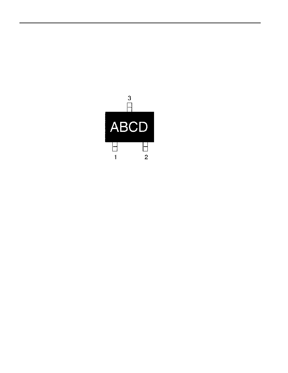
PART MARKING CODES
"A", "B", &"C" represent the Device Type.
810
-
DS1810
811 -
DS1811
812 -
DS1812
813 -
DS1813
815 -
DS1815
816 -
DS1816
817 -
DS1817
818 -
DS1818
"D" represents the Device Tolerance.
A -
5%
B -
10%
C -
15%
D -
20%
SOT-23 PACKAGE