
1 of 18
REV: 011204
Note: Some revisions of this device may incorporate deviations from published specifications known as errata. Multiple revisions of any device
may be simultaneously available through various sales channels. For information about device errata, click here:
www.maxim-ic.com/errata
.
FEATURES
§ Integrated NV SRAM, Real-Time Clock,
Crystal, Power-Fail Control Circuit, and
Lithium Energy Source
§ Clock Registers are Accessed Identically to
the Static RAM. These Registers are Resident
in the Eight Top RAM Locations.
§ Century Byte Register (i.e., Y2K Compliant)
§ Totally Nonvolatile with Over 10 Years of
Operation in the Absence of Power
§ BCD-Coded Century, Year, Month, Date,
Day, Hours, Minutes, and Seconds with
Automatic Leap-Year Compensation Valid
Up to the Year 2100
§ Battery Voltage-Level Indicator Flag
§ Power-Fail Write Protection Allows for ±10%
V
CC
Power-Supply Tolerance
§ Lithium Energy Source is Electrically
Disconnected to Retain Freshness Until
Power is Applied for the First Time
§ DIP Module Only
Standard JEDEC Byte-Wide 32k x 8 Static
RAM Pinout
§ PowerCap
Ň
Module Board Only
Surface-Mountable Package for Direct
Connection to PowerCap Containing
Battery and Crystal
Replaceable Battery (PowerCap)
Power-On Reset Output
Pin-for-Pin Compatible with Other Densities
of DS174xP Timekeeping RAM
§ Also Available in Industrial Temperature
Range: -40°C to +85°C
PIN CONFIGURATIONS
PowerCap is a registered trademark of Dallas Semiconductor.
DS1744/DS1744P
Y2K-Compliant, Nonvolatile Timekeeping RAMs
www.maxim-ic.com
PDIP Module
(700-mil Extended)
V
CC
WE
A13
A8
A9
A11
OE
A10
CE
DQ7
DQ6
DQ5
DQ4
DQ3
1
2
3
4
5
6
7
8
9
10
11
12
13
14
A14
A12
A7
A6
A5
A4
A3
A2
A1
A0
DQ0
DQ1
DQ2
GND
28
27
26
25
24
23
22
21
20
19
18
17
16
15
Dallas
Semiconductor
DS1744
1
N.C.
2
3
N.C.
N.C.
RST
V
CC
WE
OE
CE
DQ7
DQ6
DQ5
DQ4
DQ3
DQ2
DQ1
DQ0
GND
4
5
6
7
8
9
10
11
12
13
14
15
16
17
N.C.
A14
33
32
31
30
29
28
27
26
25
24
23
22
21
20
19
18
A13
A12
A11
A10
A9
A8
A7
A6
A5
A4
A3
A2
A1
A0
34
N.C.
X1
GND
V
BAT
X2
PowerCap Module Board
(Uses DS9034PCX PowerCap)
Dallas
Semiconductor
DS1744P
TOP VIEW
DS1744/DS1744P Y2K-Compliant, Nonvolatile Timekeeping RAMs
2 of 18
PIN DESCRIPTION
A0A14
- Address Input
CE
- Chip Enable
OE
- Output Enable
WE
- Write Enable
V
CC
-
Power-Supply
Input
GND
-
Ground
DQ0DQ7 - Data Input/Output
N.C.
- No Connection
RST
- Power-On Reset Output (PowerCap module board only)
X1, X2
- Crystal Connection
V
BAT
- Battery Connection
ORDERING INFORMATION
PART TEMP
RANGE
PIN-PACKAGE
VOLTAGE
(V)
TOP MARK
DS1744-70
0°C to +70°C
28 PDIP Module
5
DS1744-70
DS1744-70IND
-40°C to +85°C
28 PDIP Module
5
DS1744-70IND
DS1744P-70
0°C to +70°C
34 PowerCap*
5
DS1744P-70
DS1744P-70IND
-40°C to +85°C
34 PowerCap*
5
DS1744P-70IND
DS1744W-120
0°C to +70°C
28 DIP Module
3.3
DS1744W-120
DS1744W-120IND
-40°C to +85°C
28 DIP Module
3.3
DS1744W-120IND
DS1744WP-120
0°C to +70°C
34 PowerCap*
3.3
DS1744WP-120
DS1744WP-120IND
-40°C to +85°C
34 PowerCap*
3.3
DS1744WP-120IND
*
DS9034PCX (PowerCap) required. (Must be ordered separately.)
DESCRIPTION
The DS1744 is a full-function, year-2000-compliant (Y2KC), real-time clock/calendar (RTC) and 32k x 8
NV SRAM. User access to all registers within the DS1744 is accomplished with a byte-wide interface as
shown in Figure 1. The RTC information and control bits reside in the eight uppermost RAM locations.
The RTC registers contain century, year, month, date, day, hours, minutes, and seconds data in 24-hour
BCD format. Corrections for the date of each month and leap year are made automatically. The RTC clock
registers are double-buffered to avoid access of incorrect data that can occur during clock update cycles.
The double-buffered system also prevents time loss as the timekeeping countdown continues unabated by
access to time register data. The DS1744 also contains its own power-fail circuitry that deselects the
device when the V
CC
supply is in an out-of-tolerance condition. This feature prevents loss of data from
unpredictable system operation brought on by low V
CC
as errant access and update cycles are avoided.

DS1744/DS1744P Y2K-Compliant, Nonvolatile Timekeeping RAMs
3 of 18
Figure 1. Block Diagram
PACKAGES
The DS1744 is available in two packages (28-pin DIP and 34-pin PowerCap module). The 28-pin DIP
style module integrates the crystal, lithium energy source, and silicon all in one package. The 34-pin
PowerCap module board is designed with contacts for connection to a separate PowerCap (DS9034PCX)
that contains the crystal and battery. This design allows the PowerCap to be mounted on top of the
DS1744P after the completion of the surface-mount process. Mounting the PowerCap after the surface-
mount process prevents damage to the crystal and battery due to the high temperatures required for solder
reflow. The PowerCap is keyed to prevent reverse insertion. The PowerCap module board and PowerCap
are ordered separately and shipped in separate containers. The part number for the PowerCap is
DS9034PCX.
CLOCK OPERATIONS--READING THE CLOCK
While the double-buffered register structure reduces the chance of reading incorrect data, internal updates
to the DS1744 clock registers should be halted before clock data is read to prevent reading of data in
transition. However, halting the internal clock register updating process does not affect clock accuracy.
Updating is halted when a 1 is written into the read bit, bit 6 of the century register (Table 2). As long as a
1 remains in that position, updating is halted. After a halt is issued, the registers reflect the count, that is,
day, date, and time that was current at the moment the halt command was issued. However, the internal
clock registers of the double-buffered system continue to update so that the clock accuracy is not affected
by the access of data. All the DS1744 registers are updated simultaneously after the internal clock-register
updating process has been re-enabled. Updating is within a second after the read bit is written to 0. The
READ bit must be a 0 for a minimal of 500
ms to ensure the external registers are updated.

DS1744/DS1744P Y2K-Compliant, Nonvolatile Timekeeping RAMs
4 of 18
Table 1. Truth Table
V
CC
CE OE WE MODE DQ POWER
V
IH
X X Deselect High-Z
Standby
V
IL
X V
IL
Write Data
In
Active
V
IL
V
IL
V
IH
Read Data
Out
Active
V
CC
> V
PF
V
IL
V
IH
V
IH
Read High-Z
Active
V
SO
< V
CC
< V
PF
X X X Deselect High-Z CMOS
Standby
V
CC
< V
SO
< V
PF
X X X Deselect High-Z
Data-Retention
Mode
SETTING THE CLOCK
As shown in Table 2, bit 7 of the century register is the write bit. Setting the write bit to a 1, like the read
bit, halts updates to the DS1744 registers. The user can then load them with the correct day, date, and time
data in 24-hour BCD format. Resetting the write bit to a 0 then transfers those values to the actual clock
counters and allows normal operation to resume.
STOPPING AND STARTING THE CLOCK OSCILLATOR
The clock oscillator can be stopped at any time. To increase the shelf life, the oscillator can be turned off
to minimize current drain from the battery. The
OSC bit is the MSB (bit 7) of the seconds registers (Table
2). Setting it to a 1 stops the oscillator.
FREQUENCY TEST BIT
As shown in Table 2, bit 6 of the day byte is the frequency test bit. When the frequency test bit is set to
logic 1 and the oscillator is running, the LSB of the seconds register toggles at 512Hz. When the seconds
register is being read, the DQ0 line toggles at the 512Hz frequency as long as conditions for access remain
valid (i.e., CE low, OE low, WE high, and address for seconds register remain valid and stable).
CLOCK ACCURACY (DIP MODULE)
The DS1744 is guaranteed to keep time accuracy to within
±1 minute per month at +25°C. The RTC is
calibrated at the factory by Dallas Semiconductor using nonvolatile tuning elements, and does not require
additional calibration. For this reason, methods of field clock calibration are not available and not
necessary. Clock accuracy is also affected by the electrical environment; caution should be taken to place
the RTC in the lowest-level EMI section of the PC board layout. For additional information, refer to
Application Note 58: Crystal Considerations with Dallas Real-Time Clocks.
CLOCK ACCURACY (PowerCap MODULE)
The DS1744 and DS9034PCX are individually tested for accuracy. Once mounted together, the module
typically keeps time accuracy to within
±1.53 minutes per month (35ppm) at +25°C. Clock accuracy is
also affected by the electrical environment and caution should be taken to place the RTC in the lowest-
level EMI section of the PC board layout. For additional information, refer to Application Note 58: Crystal
Considerations with Dallas Real-Time Clocks.

DS1744/DS1744P Y2K-Compliant, Nonvolatile Timekeeping RAMs
5 of 18
Table 2. Register Map
DATA
ADDRESS
B7 B6 B5 B4 B3 B2 B1 B0
FUNCTION RANGE
7FFFF 10
Year
Year
Year
00-99
7FFFE
X X X
10
Month
Month
Month
01-12
7FFFD X X
10
Date
Date
Date 01-31
7FFFC BF FT X
X
X
Day
Day 01-07
7FFFB X X
10
Hour
Hour Hour
00-23
7FFFA X
10
Minutes
Minutes
Minutes
00-59
7FFF9
OSC
10 Seconds
Seconds
Seconds
00-59
7FFF8 W R
10
Century
Century
Century
00-39
OSC = Stop Bit
R = Read Bit
FT = Frequency Test
W = Write Bit
X = See Note
BF = Battery Flag
NOTE: All indicated "X" bits are not dedicated to any particular function and can be used as normal RAM bits.
RETRIEVING DATA FROM RAM OR CLOCK
The DS1744 is in the read mode whenever OE (output enable) is low, WE (write enable) is high, and
CE (chip enable) is low. The device architecture allows ripple-through access to any of the address
locations in the NV SRAM. Valid data is available at the DQ pins within t
AA
after the last address input is
stable, providing that the CE and OE access times and states are satisfied. If CE or OE access times and
states are not met, valid data is available at the latter of chip-enable access (t
CEA
) or at output-enable access
time (t
OEA
). The state of the DQ pins is controlled by CE and OE . If the outputs are activated before t
AA
,
the data lines are driven to an intermediate state until t
AA
. If the address inputs are changed while CE and
OE remain valid, output data remains valid for output-data hold time (t
OH
) but then goes indeterminate
until the next address access.
WRITING DATA TO RAM OR CLOCK
The DS1744 is in the write mode whenever WE and CE are in their active state. The start of a write is
referenced to the latter occurring transition of WE or CE . The addresses must be held valid throughout
the cycle. CE or WE must return inactive for a minimum of t
WR
prior to the initiation of another read or
write cycle. Data in must be valid t
DS
prior to the end of write and remain valid for t
DH
afterward. In a
typical application, the OE signal is high during a write cycle. However, OE can be active provided that
care is taken with the data bus to avoid bus contention. If OE is low prior to WE transitioning low, the
data bus can become active with read data defined by the address inputs. A low transition on WE then
disables the output t
WEZ
after WE goes active.

DS1744/DS1744P Y2K-Compliant, Nonvolatile Timekeeping RAMs
6 of 18
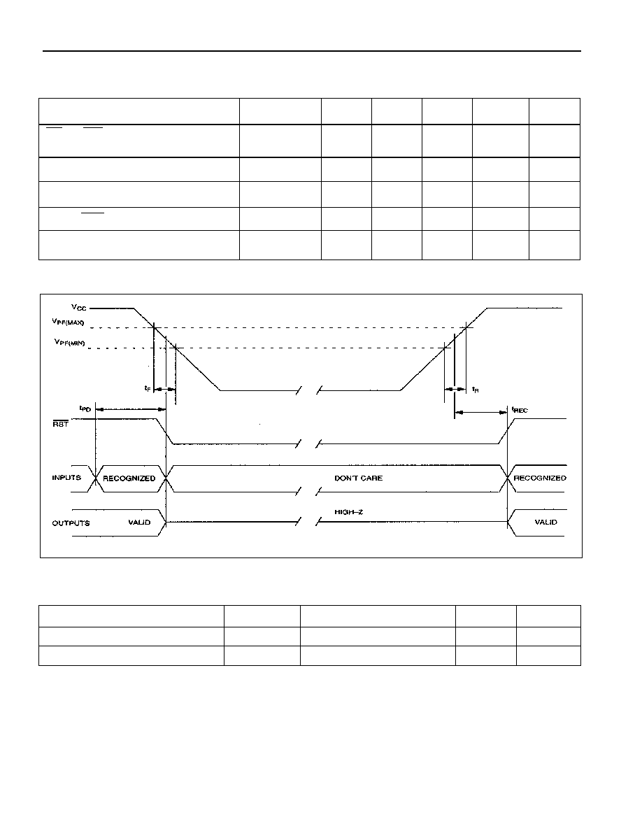
DATA-RETENTION MODE
The 5V device is fully accessible and data can be written or read only when V
CC
is greater than V
PF
.
However, when V
CC
is below the power-fail point, V
PF
(point at which write protection occurs), the
internal clock registers and SRAM are blocked from any access. At this time the power-fail reset-output
signal ( RST ) is driven active and remains active until V
CC
returns to nominal levels. When V
CC
falls
below the battery switch point V
SO
(battery supply level), device power is switched from the V
CC
pin to the
backup battery. RTC operation and SRAM data are maintained from the battery until V
CC
is returned to
nominal levels. The 3.3V device is fully accessible, and data can be written or read only when V
CC
is
greater than V
PF
.
When V
CC
falls below V
PF
access to the device is inhibited. At this time the power-fail
reset-output signal ( RST ) is driven active and remains active until V
CC
returns to nominal levels. If V
PF
is
less than V
SO
, the device power is switched from V
CC
to the backup supply (V
BAT
) when V
CC
drops below
V
PF
.
If V
PF
is greater than V
SO
, the device power is switched from V
CC
to the backup supply (V
BAT
) when
V
CC
drops below V
SO
. RTC operation and SRAM data are maintained from the battery until V
CC
is
returned to nominal levels. The RST signal is an open-drain output and requires a pullup. Except for the
RST , all control, data, and address signals must be powered down when V
CC
is powered down.
BATTERY LONGEVITY
The DS1744 has a lithium power source that is designed to provide energy for clock activity and clock and
RAM data retention when the V
CC
supply is not present. The capability of this internal power supply is
sufficient to power the DS1744 continuously for the life of the equipment in which it is installed. For
specification purposes, the life expectancy is 10 years at +25
°C with the internal clock oscillator running
in the absence of V
CC
power. Each DS1744 is shipped from Dallas Semiconductor with its lithium energy
source disconnected, guaranteeing full energy capacity. When V
CC
is first applied at a level greater than
V
PF
, the lithium energy source is enabled for battery-backup operation. Actual life expectancy of the
DS1744 is much longer than 10 years since no lithium battery energy is consumed when V
CC
is present.
BATTERY MONITOR
The DS1744 constantly monitors the battery voltage of the internal battery. The battery flag bit (bit 7) of
the day register is used to indicate the voltage-level range of the battery. This bit is not writable and should
always be a 1 when read. If a 0 is ever present, an exhausted lithium energy source is indicated, and both
the contents of the RTC and RAM are questionable.

DS1744/DS1744P Y2K-Compliant, Nonvolatile Timekeeping RAMs
7 of 18
ABSOLUTE MAXIMUM RATINGS
Voltage Range on Any Pin Relative to Ground.........................................................................-0.3V to +6.0V
Operating Temperature Range.............................................................................................-40°C to +85°C
Storage Temperature Range...............................................................................................-40°C to +85°C
Soldering Temperature....................................................See IPC/JEDEC J-STD-020A (DIP Package) (Note 7)
This is a stress rating only and functional operation of the device at these or any other condition beyond those indicated in the
operation sections of this specification is not implied. Exposure to absolute maximum rating conditions for extended periods of
time can affect reliability.
OPERATING RANGE
RANGE TEMP
RANGE V
CC
Commercial
0°C to +70°C
3.3V
±10% or 5V ±10%
Industrial
-40°C to +85°C
3.3V
±10% or 5V ±10%
RECOMMENDED DC OPERATING CONDITIONS
(T
A
= Over the operating range)
PARAMETER SYMBOL
MIN
TYP
MAX
UNITS
NOTES
V
IH
2.2
V
CC
+ 0.3V
V
1
Logic 1 Voltage (All Inputs)
V
CC
= 5V
±10%
V
CC
= 3.3V
±10%
V
IH
2.0
V
CC
+ 0.3V
V
V
IL
-0.3
0.8 V
Logic 0 Voltage (All Inputs)
V
CC
= 5V
±10%
V
CC
= 3.3V
±10%
V
IL
0.3
0.6 V
1
DC ELECTRICAL CHARACTERISTICS
(V
CC
= 5.0V
±10%, T
A
= Over the operating range.)
PARAMETER SYMBOL
MIN
TYP
MAX
UNITS
NOTES
Active Supply Current
I
CC
75
mA
2,
3
TTL Standby Current
( CE = V
IH
)
I
CC1
6
mA
2,
3
CMOS Standby Current
( CE
ł V
CC
- 0.2V)
Icc
2
4
mA
2,
3
Input Leakage Current (Any
Input)
I
IL
-1 +1
mA
Output Leakage Current
(Any Output)
I
OL
-1 +1
mA
Output Logic 1 Voltage
(I
OUT
= -1.0mA)
V
OH
2.4 1
Output Logic 0 Voltage
(I
OUT
= +2.1mA)
V
OL
0.4
1
Write Protection Voltage
V
PF
4.25 4.50
V 1
Battery Switchover Voltage
V
SO
V
BAT
1,
4
DS1744/DS1744P Y2K-Compliant, Nonvolatile Timekeeping RAMs
8 of 18
DC ELECTRICAL CHARACTERISTICS
(V
CC
= 3.3V
±10%, T
A
= Over the operating range.)
PARAMETER SYMBOL
MIN
TYP
MAX
UNITS
NOTES
Active Supply Current
I
CC
30
mA
2,
3
TTL Standby Current
( CE = V
IH
)
I
CC1
2
mA
2,
3
CMOS Standby Current
( CE
ł V
CC
- 0.2V)
I
CC2
2
mA
2,
3
Input Leakage Current (Any
Input)
I
IL
-1 +1
mA
Output Leakage Current
(Any Output)
I
OL
-1 +1
mA
Output Logic 1 Voltage
(I
OUT
= -1.0mA)
V
OH
2.4
1
Output Logic 0 Voltage
(I
OUT
= +2.1mA)
V
OL
0.4
1
Write Protection Voltage
V
PF
2.80 2.97
V 1
Battery Switchover Voltage
V
SO
V
BAT
or
V
PF
V 1,
4
AC CHARACTERISTICS--READ CYCLE (5V)
(V
CC
= 5.0V
±10%,
T
A
=
Over the operating range.)
PARAMETER SYMBOL
MIN
TYP
MAX
UNITS
NOTES
Read Cycle Time
t
RC
70 ns
Address Access Time
t
AA
70
ns
CE to DQ Low-Z
t
CEL
5 ns
CE Access Time
t
CEA
70
ns
CE Data Off Time
t
CEZ
25
ns
OE to DQ Low-Z
t
OEL
5 ns
OE Access Time
t
OEA
35
ns
OE Data Off Time
t
OEZ
25
ns
Output Hold from Address
t
OH
5 ns

DS1744/DS1744P Y2K-Compliant, Nonvolatile Timekeeping RAMs
9 of 18
AC CHARACTERISTICS--READ CYCLE (3.3V)
(V
CC
= 3.3V
±10%, T
A
= Over the operating range.)
PARAMETER SYMBOL
MIN
TYP
MAX
UNITS
NOTES
Read Cycle Time
t
RC
120 ns
Address Access Time
t
AA
120
ns
CE to DQ Low-Z
t
CEL
5 ns
CE Access Time
t
CEA
120
ns
CE Data Off Time
t
CEZ
40 ns
OE to DQ Low-Z
t
OEL
5 ns
OE Access Time
t
OEA
100
ns
OE Data Off Time
t
OEZ
35 ns
Output Hold from Address
t
OH
5 ns
READ CYCLE TIMING DIAGRAM
DS1744/DS1744P Y2K-Compliant, Nonvolatile Timekeeping RAMs
10 of 18
AC CHARACTERISTICS--WRITE CYCLE (5V)
(V
CC
= 5.0V
±10%, T
A
= Over the operating range.)
PARAMETER SYMBOL
MIN
TYP
MAX
UNITS
NOTES
Write Cycle Time
t
WC
70
ns
Address Setup Time
t
AS
0
ns
WE Pulse Width
t
WEW
50
ns
CE Pulse Width
t
CEW
60
ns
Data Setup Time
t
DS
30
ns
Data Hold Time
t
DH1
0
ns 8
Data Hold Time
t
DH2
0
ns 9
Address Hold Time
t
AH1
5
ns 8
Address Hold Time
t
AH2
5
ns 9
WE Data Off Time
t
WEZ
25 ns
Write Recovery Time
t
WR
5
ns
AC CHARACTERISTICS--WRITE CYCLE (3.3V)
(V
CC
= 3.3V
±10%, T
A
= Over the operating range.)
PARAMETER SYMBOL
MIN
TYP
MAX
UNITS
NOTES
Write Cycle Time
t
WC
120
ns
Address Setup Time
t
AS
0
120 ns
WE Pulse Width
t
WEW
100
ns
CE Pulse Width
t
CEW
110
ns
CE and CE2 Pulse Width
t
CEW
110
ns
Data Setup Time
t
DS
80
ns
Data Hold Time
t
DH1
0
ns 8
Data Hold Time
t
DH2
0
ns 9
Address Hold Time
t
AH1
0
ns 8
Address Hold Time
t
AH2
10
ns 9
WE Data Off Time
t
WEZ
40 ns
Write Recovery Time
t
WR
10
ns
DS1744/DS1744P Y2K-Compliant, Nonvolatile Timekeeping RAMs
11 of 18
WRITE CYCLE TIMING DIAGRAM, WRITE-ENABLE CONTROLLED
WRITE CYCLE TIMING DIAGRAM, CHIP-ENABLE CONTROLLED

DS1744/DS1744P Y2K-Compliant, Nonvolatile Timekeeping RAMs
12 of 18
POWER-UP/DOWN AC CHARACTERISTICS (5V)
(V
CC
= 5.0V
±10%, T
A
= Over the operating range.)
PARAMETER SYMBOL
MIN
TYP
MAX
UNITS
NOTES
CE or WE at V
IH
Before Power-Down
t
PD
0
ms
V
CC
Fall Time: V
PF(MAX)
to V
PF(MIN)
t
F
300
ms
V
CC
Fall Time: V
PF(MIN)
to V
SO
t
FB
10
ms
V
CC
Rise Time: V
PF(MIN)
to V
PF(MAX)
t
R
0
ms
Power-Up Recover Time
t
REC
35
ms
Expected Data-Retention Time
(Oscillator ON)
t
DR
10
years
5,
6
POWER-UP/DOWN TIMING (5V DEVICE)
DS1744/DS1744P Y2K-Compliant, Nonvolatile Timekeeping RAMs
13 of 18
POWER-UP/DOWN CHARACTERISTICS (3.3V)
(V
CC
= 3.3V
±10%, T
A
= Over the operating range.)
PARAMETER SYMBOL
MIN
TYP
MAX
UNITS
NOTES
CE or WE at V
IH
, Before Power-
Down
t
PD
0
ms
V
CC
Fall Time: V
PF(MAX)
to V
PF(MIN)
t
F
300
ms
V
CC
Rise Time: V
PF(MIN)
to V
PF(MAX)
t
R
0
ms
V
PF
to RST High
t
REC
35
ms
Expected Data-Retention Time
(Oscillator ON)
t
DR
10
years
5,
6
POWER-UP/DOWN WAVEFORM TIMING (3.3V DEVICE)
CAPACITANCE
(T
A
= +25°C)
PARAMETER SYMBOL
MIN
TYP
MAX
UNITS
NOTES
Capacitance On All Input Pins
C
IN
14
pF
Capacitance On All Output Pins
C
O
10
pF

DS1744/DS1744P Y2K-Compliant, Nonvolatile Timekeeping RAMs
14 of 18
AC TEST CONDITIONS
Output Load: 50pF + 1TTL Gate
Input Pulse Levels: 0 to 3.0V
Timing Measurement Reference Levels:
Input: 1.5V
Output: 1.5V
Input Pulse Rise and Fall Times: 5ns
NOTES:
1) Voltages are referenced to ground.
2) Typical values are at +25
°C and nominal supplies.
3) Outputs are open.
4) Battery switchover occurs at the lower of either the battery terminal voltage or V
PF
.
5) Data-retention time is at +25
°C.
6) Each DS1744 has a built-in switch that disconnects the lithium source until the user first applies V
CC
.
The expected t
DR
is defined for DIP modules and assembled PowerCap modules as a cumulative time
in the absence of V
CC
starting from the time power is first applied by the user.
7) RTC modules (DIP) can be successfully processed through conventional wave-soldering techniques as
long as temperature exposure to the lithium energy source contained within does not exceed +85
°C.
Post-solder cleaning with water-washing techniques is acceptable, provided that ultrasonic vibration is
not used.
In addition, for the PowerCap:
a. ) Dallas Semiconductor recommends that PowerCap module bases experience one pass through
solder reflow oriented with the label side up ("live-bug").
b.) Hand soldering and touch-up: Do not touch or apply the soldering iron to leads for more than
3 seconds. To solder, apply flux to the pad, heat the lead frame pad, and apply solder. To
remove the part, apply flux, heat the lead frame pad until the solder reflows, and use a solder
wick to remove solder.
8) t
AH1
, t
DH1
are measured from
WE going high.
9) t
AH2
, t
DH2
are measured from
CE going high.
DS1744/DS1744P Y2K-Compliant, Nonvolatile Timekeeping RAMs
15 of 18
PACKAGE INFORMATION
(The package drawing(s) in this data sheet may not reflect the most current specifications. For the latest package
outline information, go to
www.maxim-ic.com/DallasPackInfo
.)
28-PIN
PKG DIM
MIN MAX
IN 1.470 1.490
A
MM 37.34 37.85
IN 0.675 0.740
B
MM 17.75 18.80
IN 0.335 0.355
C
MM 8.51 9.02
IN 0.075 0.105
D
MM 1.91 2.67
IN 0.015 0.030
E
MM 0.38 0.76
IN 0.140 0.180
F
MM 3.56 4.57
IN 0.090 0.110
G
MM 2.29 2.79
IN 0.590 0.630
H
MM 14.99 16.00
IN 0.010 0.018
J
MM 0.25 0.45
IN 0.015 0.025
K
MM 0.43 0.58

DS1744/DS1744P Y2K-Compliant, Nonvolatile Timekeeping RAMs
16 of 18
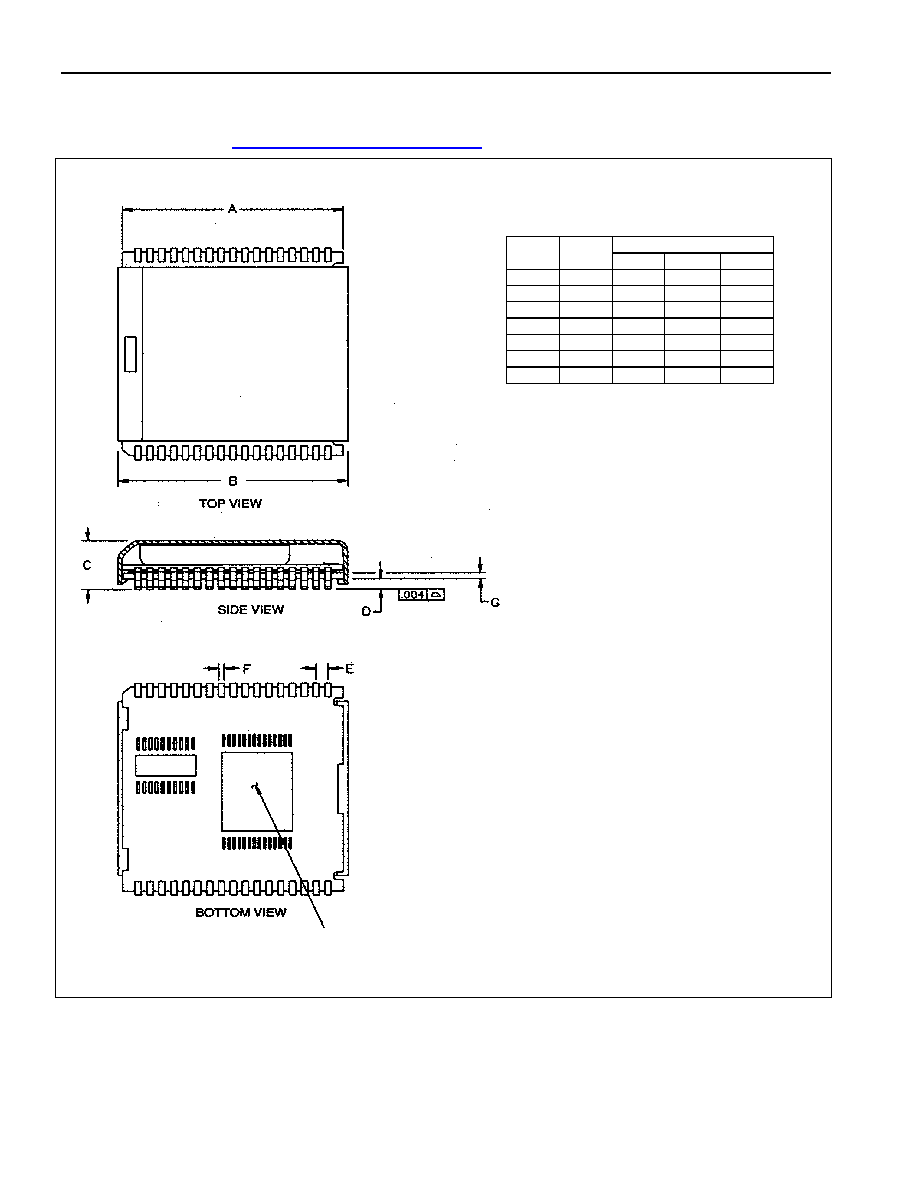
PACKAGE INFORMATION (continued)
(The package drawing(s) in this data sheet may not reflect the most current specifications. For the latest package
outline information, go to
www.maxim-ic.com/DallasPackInfo
.)
34-PIN PowerCap
MODULE
PKG DIM
MIN NOM MAX
A IN
0.920
0.925
0.930
B IN
0.980
0.985 0.990
C IN
-- -- 0.080
D IN
0.052
0.055 0.058
E IN
0.048
0.050 0.052
F IN
0.015
0.020 0.025
G IN
0.025
0.027 0.030
NOTE: DALLAS SEMICONDUCTOR RECOMMENDS THAT POWERCAP MODULE BASES
EXPERIENCE ONE PASS THROUGH SOLDER REFLOW ORIENTED WITH THE LABE
SIDE UP ("LIVE-BUG").
NOTE: HAND SOLDERING AND TOUCH-UP: DO NOT TOUCH OR APPLY THE
SOLDERING IRON TO LEADS FOR MORE THAN 3 SECONDS. TO SOLDER, APPLY FLUX
TO THE PAD, HEAT THE LEAD FRAME PAD, AND APPLY SOLDER. TO REMOVE THE
PART, APPLY FLUX, HEAT THE LEAD FRAME PAD UNTIL THE SOLDER REFLOWS, AND
USE A SOLDER WICK TO REMOVE SOLDER.
COMPONENTS AND PLACEMENT MAY VARY FROM EACH DEVICE TYPE.
DS1744/DS1744P Y2K-Compliant, Nonvolatile Timekeeping RAMs
17 of 18
PACKAGE INFORMATION (continued)
(The package drawing(s) in this data sheet may not reflect the most current specifications. For the latest package
outline information, go to
www.maxim-ic.com/DallasPackInfo
.)
34-PIN
PKG DIM
MIN NOM MAX
A IN
0.920
0.925
0.930
B IN
0.955 0.960 0.965
C IN
0.240 0.245 0.250
D IN
0.052 0.055 0.058
E IN
0.048 0.050 0.052
F IN
0.015 0.020 0.025
G IN
0.020 0.025 0.030
COMPONENTS AND PLACEMENT MAY VARY FROM EACH DEVICE TYPE.
DS1744P WITH DS9034PCX ATTACHED
DS1744/DS1744P Y2K-Compliant, Nonvolatile Timekeeping RAMs
Maxim/Dallas Semiconductor cannot assume responsibility for use of any circuitry other than circuitry entirely embodied in a Maxim/Dallas Semiconductor product.
No circuit patent licenses are implied. Maxim/Dallas Semiconductor reserves the right to change the circuitry and specifications without notice at any time.
Ma xi m I nt e gr at e d Pr o du ct s, 1 2 0 S a n G abr i el Dr i ve, S un n yv al e, C A 94 0 8 6 40 8- 7 37- 7 60 0
© 2004 Maxim Integrated Products
· Printed USA
18 of 18
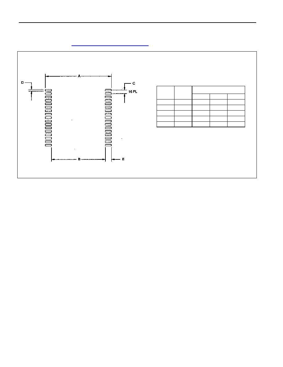
PACKAGE INFORMATION (continued)
(The package drawing(s) in this data sheet may not reflect the most current specifications. For the latest package
outline information, go to
www.maxim-ic.com/DallasPackInfo
.)
PowerCap MODULE
PKG DIM
MIN NOM MAX
A IN --
1.050
--
B IN
--
0.826 --
C IN
--
0.050 --
D IN
--
0.030 --
E IN
--
0.112 --
RECOMMENDED POWERCAP MODULE LAND PATTERN