E
Copyright 1995 by Dallas Semiconductor Corporation.
All Rights Reserved. For important information regarding
patents and other intellectual property rights, please refer to
Dallas Semiconductor data books.
DS1385/DS1387
RAMified Real Time Clock 4K x 8
DS1385/DS1387
012496 1/20
FEATURES
À
Upgraded IBM AT computer clock/calendar with
4K x 8 extended RAM
À
Totally nonvolatile with over 10 years of operation in
the absence of power
À
Counts seconds, minutes, hours, day of the week,
date, month and year with leap year compensation
À
Binary or BCD representations of time, calendar and
alarm
À
12¡ or 24¡hour clock with AM and PM in 12¡hour
mode
À
Daylight Savings Time option
À
Multiplex bus for pin efficiency
À
Interfaced with software as 64 user RAM locations
plus 4K x 8 of static RAM
¡ 14¡bytes of clock and control registers
¡ 50¡bytes of general purpose RAM
¡ 4K x 8 SRAM accessible by using separate con-
trol pins
À
Programmable square wave output signal
À
Bus¡compatible interrupt signals (IRQ)
À
Three interrupts are separately software¡maskable
and testable:
¡ Time¡of¡day alarm once/second to once/day
¡ Periodic rates from 122
Á
s to 500 ms
¡ End¡of¡clock update cycle
À
Available as chip (DS1385 or DS1385S) or stand
alone module with embedded lithium battery and
crystal (DS1387)
ORDERING INFORMATION
DS1385
RTC Chip; 24¡pin DIP
DS1385S
RTC Chip; 28¡pin SOIC
DS1387
RTC Module; 24¡pin DIP
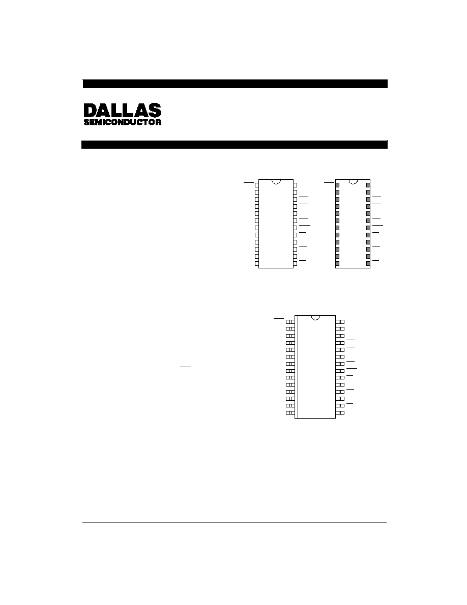
PIN ASSIGNMENT
V
CC
SQW
AS0
AS1
NC
IRQ
WER
RD
NC
WR
ALE
CS
OER
NC
NC
AD0
AD1
AD2
AD3
AD4
AD5
AD6
AD7
GND
1
2
3
4
5
6
7
8
9
10
11
12
24
23
22
21
20
19
18
17
16
15
14
13
V
CC
SQW
NC
AS0
AS1
V
BAT
IRQ
WER
RD
BGND
WR
ALE
CS
NC
OER
X1
X2
NC
AD0
AD1
AD2
AD3
AD4
AD5
AD6
AD7
NC
GND
1
2
3
4
5
6
7
8
9
10
11
12
13
14
28
27
26
25
24
23
22
21
20
19
18
17
16
15
DS1387 24¡PIN
ENCAPSULATED PACKAGE
(740 MIL FLUSH)
DS1385S 28¡PIN SOIC
(330 MIL)
V
CC
SQW
AS0
AS1
V
BAT
IRQ
WER
RD
GND
WR
ALE
CS
OER
X1
X2
AD0
AD1
AD2
AD3
AD4
AD5
AD6
AD7
GND
1
2
3
4
5
6
7
8
9
10
11
12
24
23
22
21
20
19
18
17
16
15
14
13
DS1385 24¡PIN DIP
(600 MIL)

DS1385/DS1387
012496 2/20
PIN DESCRIPTION
OER
¡ RAM Output Enable
X1
¡ Crystal Input
X2
¡ Crystal Output
AD0-AD7
¡ Mux'ed Address/Data Bus
CS
¡ RTC Chip Select Input
ALE
¡ RTC Address Strobe
WR
¡ RTC Write Data Strobe
RD
¡ RTC Read Data Strobe
WER
¡ RAM Write Data Strobe
IRQ
¡ Interrupt Request Output (open
drain)
AS1
¡ RAM Upper Address Strobe
AS0
¡ RAM Lower Address Strobe
SQW
¡ Square Wave Output
V
CC
¡ +5V Supply
GND
¡ Ground
V
BAT
¡ Battery + Supply
BGND
¡ Battery Ground
NC
¡ No Connection
DESCRIPTION
The DS1385/DS1387 RAMified Real Time Clocks
(RTCs) are upward¡compatible successors to the in-
dustry standard DS1285/DS1287 RTC's for PC applica-
tions. In addition to the basic DS1285/DS1287 RTC
functions, 4K bytes of on¡chip nonvolatile RAM have
been added.
The RTC functions include a time¡of¡day clock, a one-
hundred year calendar, time¡of¡day interrupt, periodic
interrupts, and an end¡of¡clock update cycle interrupt.
In addition, 50¡bytes of user NV RAM are provided with-
in this basic RTC function which can be used to store
configuration data. The clock and user RAM are main-
tained in the absence of system V
CC
by a lithium battery.
The 4K x 8 additional NV RAM is provided to store a
much larger amount of system configuration data than is
possible within the original 50¡byte area. This RAM is
accessed via control signals separate from the RTC,
and is also maintained as nonvolatile storage from the
lithium battery.
OPERATION
The block diagram in Figure 1 shows the pin connec-
tions with the major internal functions of the
DS1385/DS1387. The following paragraphs describe
the function of each pin.
SIGNAL DESCRIPTIONS
GND, V
CC
¡ DC power is provided to the device on
these pins. V
CC
is the +5 volt input. When 5 volts are
applied within normal limits, the device is fully accessi-
ble and data can be written and read. When V
CC
is be-
low 4.25 volts typical, reads and writes are inhibited.
However, the timekeeping function continues unaf-
fected by the lower input voltage. As V
CC
falls below 3
volts typical, the RAM and timekeeper are switched
over to the energy source connected to the V
BAT
pin in
the case of the DS1385, or to the internal battery in the
case of the DS1387. The timekeeping function main-
tains an accuracy of
▒
1 minute per month at 25
░
C re-
gardless of the voltage input on the V
CC
pin.
SQW (Square Wave Output) ¡ The SQW pin can output
a signal from one of 13 taps provided by the 15 internal
divider stages of the real time clock. The frequency of the
SQW pin can be changed by programming Register A as
shown in Table 2. The SQW signal can be turned on and
off using the SQWE bit in Register B. The SQW signal is
not available when V
CC
is less than 4.25 volts typical.
AD0¡AD7 (Multiplexed Bi¡directional Address/Data
Bus) ¡ Multiplexed buses save pins because address
information and data information time share the same
signal paths. The addresses are present during the first
portion of the bus cycle and the same pins and signal
paths are used for data in the second portion of the
cycle. Address/data multiplexing does not slow the ac-
cess time of the DS1385/DS1387 since the bus change
from address to data occurs during the internal RAM ac-
cess time. Addresses must be valid prior to the latter
portion of ALE, AS0, or AS1, at which time the
DS1385/DS1387 latches the address from AD0 to AD7.
Valid write data must be present and held stable during
the latter portion of the WR or WER pulses. In a read
cycle, the DS1385/DS1387 outputs eight bits of data
during the latter portion of the RD or OER pulses. The
read cycle is terminated and the bus returns to a high im-
pedance state as RD or OER transitions high.
ALE (RTC Address Strobe Input) ¡ A positive going
address strobe pulse serves to demultiplex the bus.
The falling edge of ALE causes the RTC address to be
latched within the DS1385/DS1387.
RD (RTC Read Input) ¡ RD identifies the time period
when the DS1385/DS1387 drives the bus with RTC
read data. The RD signal is an enable signal for the out-
put buffers of the clock.

DS1385/DS1387
012496 3/20
DS1385/DS1387 BLOCK DIAGRAM Figure 1
OSC
POWER
SWITCH
AND
WRITE
PROTECT
V
CC
BUFFER
ENABLE
V
CC
PERIODIC INTERRUPT/SQUARE WAVE
SELECTOR
SQUARE
WAVE OUT
SQW
IRQ
DOUBLE
BUFFERED
REGISTERS A, B, C, D
CLOCK, CALENDAR,
AND ALARM
BCD/BINARY
INCREMENT
CLOCK/
CALENDAR
UPDATE
BUS
INTERFACE
ALE
RD
WR
AD0-AD7
X1
X2
V
CC
CS
POK
+
¡
+3V
V
BAT
CS
AS1
AS0
WER
USER RAM
50 BYTES
ADDRESS HIGH
BYTE LATCH
ADDRESS LOW
BYTE LATCH
DATA LATCH
NONVOLATILE RAM
4K X 8
64
8
64
OER
CONTROL

DS1385/DS1387
012496 4/20
WR (RTC Write Input) ¡The WR signal is an active low
signal. The WR signal defines the time period during
which data is written to the addressed clock register.
CS (RTC Chip Select Input) ¡ The Chip Select signal
must be asserted low during a bus cycle for the RTC
portion of the DS1385/DS1387 to be accessed. CS
must be kept in the active state during RD and WR tim-
ing. Bus cycles which take place without asserting CS
will latch addresses but no access will occur.
IRQ (Interrupt Request Output) ¡ The IRQ pin is an
active low output of the DS1385/DS1387 that can be
tied to an interrupt input on a processor. The IRQ output
remains low as long as the status bit causing the inter-
rupt is present and the corresponding interrupt¡enable
bit is set. To clear the IRQ pin, the application program
normally reads the C register.
When no interrupt conditions are present, the IRQ level
is in the high impedance state. Multiple interrupting de-
vices can be connected to an IRQ bus. The IRQ bus is
an open drain output and requires an external pull¡up
resistor.
AS0 (RAM Address Strobe Zero) ¡ The rising edge of
AS0 latches the lower eight bits of the 4K x 8 RAM ad-
dress.
AS1 (RAM Address Strobe One) ¡ The rising edge of
AS1 latches the upper four bits of the 4K x 8 RAM ad-
dress.
OER (RAM Output Enable) ¡ OER is active low and
identifies the time period when the DS1385/DS1387
drives the bus with RAM read data.
WER (RAM Write Enable) ¡ WER is an active low sig-
nal and is used to perform writes to the 4K x 8 RAM por-
tion of the DS1385/DS1387.
(DS1385 ONLY)
X1, X2 ¡ Connections for a standard 32.768 KHz quartz
crystal. When ordering, request a load capacitance of 6
pF. The internal oscillator circuitry is designed for opera-
tion with a crystal having a specified load capacitance
(CL) of 6 pF. The crystal is connected directly to the X1
and X2 pins. There is no need for external capacitors or
resistors. Note: X1 and X2 are very high impedance
nodes. It is recommended that they and the crystal be
guard¡ringed with ground and that high frequency sig-
nals be kept away from the crystal area. For more
information on crystal selection and crystal layout con-
siderations, please consult Application Note 58, "Crys-
tal Considerations with Dallas Real Time Clocks".
V
BAT
, BGND ¡ Battery input for any standard 3 volt lithi-
um cell or other energy source. Battery voltage must be
held between 2.5 and 3.7 volts for proper operation. The
nominal write protect trip point voltage is set by the inter-
nal circuitry and is 4.25 volts typical. A maximum load of
1
Á
A at 25
░
C and 3.0V on V
BAT
should in the absence of
power be used to size the external energy source.
The battery should be connected directly to the V
BAT
pin.
A diode must not be placed in series with the battery to
the V
BAT
pin. Furthermore, a diode is not necessary
because reverse charging current protection circuitry is
provided internal to the device and has passed the
requirements of Underwriters Laboratories for UL listing
(E99151).
ADDRESS MAP
The address map of the DS1385/DS1387 is shown in
Figure 2. The address map consists of the RTC and the
4K X 8 NV SRAM section. The RTC section contains
50¡bytes of user RAM, 10¡bytes of RAM that contain
the RTC time, calendar, and alarm data, and 4¡bytes
which are used for control and status. All 64¡bytes can
be directly written or read except for the following:
1. Registers C and D are read-only.
2. Bit¡7 of Register A is read-only.
3. The high order bit of the seconds byte is read-only.
RTC (REAL TIME CLOCK)
The RTC function is the same as the DS1287 Real Time
Clock. Access to the RTC is accomplished with four
controls: ALE, RD, WR and CS. The RTC is the same in
the DS1287 with the following exceptions:
1. The MOT pin on the DS1285/DS1287 is not present
on the DS1385/DS1387. The bus selection capabili-
ty of the DS1285/DS1287 has been eliminated. Only
the Intel bus interface timing is applicable.
2. The RESET pin on the DS1285/DS1287 is not pres-
ent on the DS1385/DS1387. The DS1385/DS1387
will operate the same as the DS1285/DS1287 with
RESET tied to V
CC
.

DS1385/DS1387
012496 5/20
ADDRESS MAP DS1385/DS1387 Figure 2
0
00
13
14
0D
0E
14¡BYTES
63
3F
0
1
2
3
4
5
6
7
8
9
10
11
12
13
SECONDS
SECONDS ALARM
MINUTES
MINUTES ALARM
HOURS
HOURS ALARM
DAY OF THE WEEK
DAY OF THE MONTH
MONTH
YEAR
REGISTER A
REGISTER B
REGISTER C
REGISTER D
BINAR
Y
OR BCD INPUTS
50¡BYTES
USER RAM
0
4096
000
FFF
4K X 8
NV SRAM
TIME, CALENDAR AND ALARM LOCATIONS
The time and calendar information is obtained by read-
ing the appropriate register bytes shown in Table 1. The
time, calendar and alarm are set or initialized by writing
the appropriate register bytes. The contents of the time,
calendar and alarm registers can be either Binary or
Binary¡Coded Decimal (BCD) format. Table 1 shows
the binary and BCD formats of the twelve time, calendar
and alarm locations.
Before writing the internal time, calendar and alarm reg-
isters, the SET bit in Register B should be written to a
logic one to prevent updates from occurring while ac-
cess is being attempted. Also at this time, the data for-
mat (binary or BCD), should be set via the data mode bit
(DM) of Register B. All time, calendar and alarm regis-
ters must use the same data mode. The set bit in Regis-
ter B should be cleared after the data mode bit has been
written to allow the real¡time clock to update the time
and calendar bytes.
Once initialized, the real¡time clock makes all updates
in the selected mode. The data mode cannot be
changed without reinitializing the ten data bytes. The
24/12 bit cannot be changed without reinitializing the
hour locations. When the 12¡hour format is selected,
the high order bit of the hours byte represents PM when
it is a logic one. The time, calendar and alarm bytes are
always accessible because they are double buffered.
Once per second the 10¡bytes are advanced by one
second and checked for an alarm condition. If a read of
the time and calendar data occurs during an update, a
problem exists where seconds, minutes, hours, etc.
may not correlate. The probability of reading incorrect
time and calendar data is low. Several methods of
avoiding any possible incorrect time and calendar reads
are covered later in this text.
The three alarm bytes can be used in two ways. First,
when the alarm time is written in the appropriate hours,
minutes and seconds alarm locations, the alarm inter-
rupt is initiated at the specified time each day if the alarm
enable bit is high. The second method is to insert a
"don't care" state in one or more of the three alarm bytes.
The "don't care" code is any hexadecimal value from C0
to FF. The two most significant bits of each byte set the
"don't care" condition when at logic 1. An alarm will be
generated each hour when the "don't care" bits are set in
the hours byte. Similarly, an alarm is generated every
minute with "don't care" codes in the hours and minute
alarm bytes. The "don't care" codes in all three alarm
bytes create an interrupt every second.