DS1233M
EconoReset
DS1233M
022698 1/4
FEATURES
·
Automatically restarts microprocessor after power
failure
·
Maintains reset for 350 ms after V
CC
returns to an
in-tolerance condition
·
Reduces need for discrete components
·
Precision temperature-compensated voltage refer-
ence and voltage sensor
·
Low-cost TO-92 package or surface mount 8pin
SOIC packages available
·
Internal 5 K
pull-up resistor
·
Compatible with Motorola 68XXX series and HC16
Microprocessors
·
Pin function compatible with the Motorola MC33064,
MC34064, MC33164, and MC34164
·
Operating temperature of 40
°
C to +85
°
C
PIN ASSIGNMENT
DALLAS
1
2
3
1
2
3
DS1233
Econo
Reset
DS1233M
TO-92 Package
See Mech. Drawings
Section
8
7
6
5
1
2
3
4
RST
V
CC
NC
GND
NC
NC
NC
NC
DS1233M 8PIN SOIC
(150 MIL)
See Mech. Drawings
Section
PIN DESCRIPTIONS
TO92
1
RST
Active Low Reset Output
2
V
CC
Power Supply
3
GND
Ground
8Pin SOIC
RST
Active Low Reset Output
V
CC
Power Supply
NC
No Connect
GND
Ground
DESCRIPTION
The DS1233M EconoReset uses a precision tempera-
ture compensated reference and comparator circuit to
monitor the status of the power supply (V
CC
). When an
out-of-tolerance condition is detected, an internal power
fail signal is generated which forces reset to the active
(low) state. When V
CC
returns to an in-tolerance condi-
tion, the reset signal is kept in the active state for ap-
proximately 350 ms to allow the power supply and pro-
cessor to stabilize.
DS1233M
022698 2/4
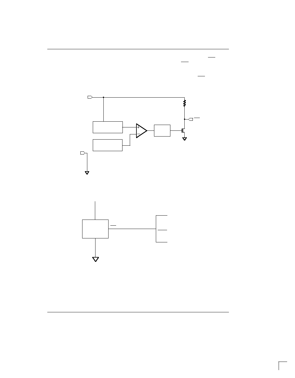
OPERATION POWER MONITOR
The DS1233M provides the functions of detecting
out-of-tolerance power supply conditions and warning a
processor-based system of impending power failure.
When V
CC
is detected as out-of-tolerance, as defined
by the tolerance of the part selected, the RST signal is
asserted. On power-up, RST is kept active for approxi-
mately 350 ms after the power supply has reached the
selected tolerance. This allows the power supply and
microprocessor to stabilize before RST is released.
BLOCK DIAGRAM Figure 1
Vcc TOLERANCE
AND BIAS
T.C. REFERENCE
350 ms
DELAY
GROUND
RST
V
CC
5K
APPLICATION EXAMPLE Figure 2
VCC
MICROPROCESSOR
RST
RESET
DS1233M

DS1233M
022698 4/4
ABSOLUTE MAXIMUM RATINGS*
Voltage on V
CC
Pin Relative to Ground
-0.5V to +7.0V
Voltage on I/O Relative to Ground
0.5V to V
CC
+ 0.5V
Operating Temperature
40
°
C to +85
°
C
Storage Temperature
-55
°
C to +125
°
C
Soldering Temperature
260
°
C for 10 seconds
* This is a stress rating only and functional operation of the device at these or any other conditions above those
indicated in the operation sections of this specification is not implied. Exposure to absolute maximum rating
conditions for extended periods of time may affect reliability.
RECOMMENDED DC OPERATING CONDITIONS
(40
°
C to +85
°
C)
PARAMETER
SYMBOL
MIN
TYP
MAX
UNITS
NOTES
Supply Voltage
V
CC
1.2
5.5
V
1
DC ELECTRICAL CHARACTERISTICS
(40
°
C to +85
°
C; V
CC
= 1.2V to 5.5V)
PARAMETER
SYMBOL
MIN
TYP
MAX
UNITS
NOTES
Output Voltage @ 500
µ
A
V
OH
V
CC
0.5V
V
CC
0.1V
V
1
Output Current @ 0.4V
I
OL
+8
mA
2, 3
Operating Current
I
CC
50
µ
A
4
V
CC
Trip Point (DS1233M5)
V
CCTP
4.25
4.375
4.49
V
1
V
CC
Trip Point (DS1233M55)
V
CCTP
4.5
4.625
4.75
V
1
V
CC
Trip Point (DS1233M3)
V
CCTP
2.64
2.72
2.8
V
1
Output Capacitance
C
OUT
10
pF
Internal Pull-Up Resistor
R
P
3.75
5
6.50
K
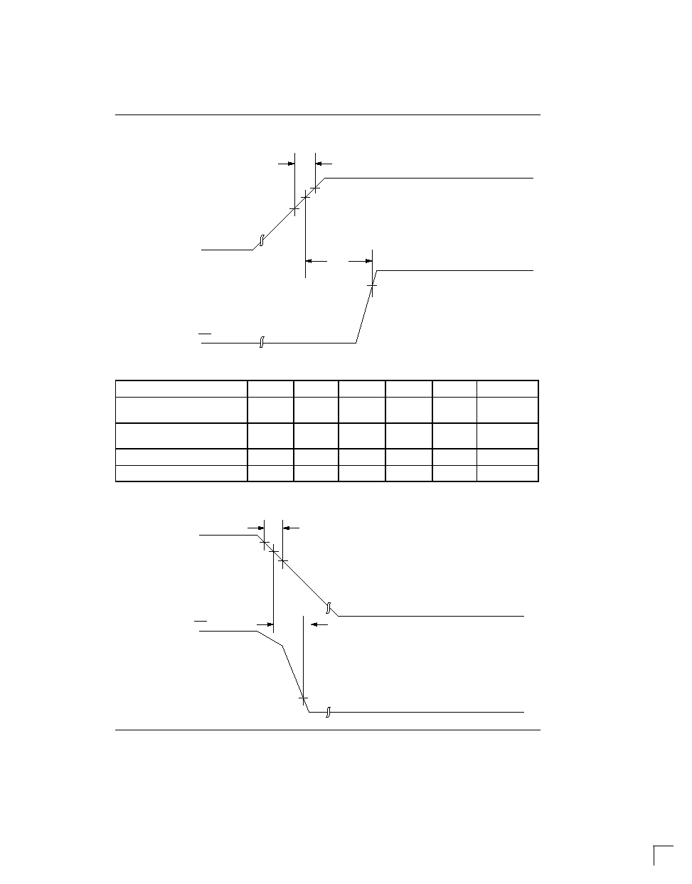
AC ELECTRICAL CHARACTERISTICS
(40
°
C to +85
°
C; V
CC
= 1.2V to 5.5V)
PARAMETER
SYMBOL
MIN
TYP
MAX
UNITS
NOTES
Reset Active Time
t
RST
200
350
500
ms
V
CC
Detect to RST
t
RPD
2
10
µ
s
V
CC
Slew Rate (V
HTL
V
LTL
)
t
F
300
µ
s
V
CC
Slew Rate (V
LTL
V
HTL
)
t
R
0
ns
V
CC
detect to RST
t
RPU
200
350
500
ms
5
NOTES:
1. All voltages are referenced to ground.
2. Measured with V
CC
2.7V.
3. A 1K
external resistor may be required in some applications for proper operation of the microprocessor
reset control circuit.
4. Measured with outputs open.
5. t
R
= 5
µ
s.