CYStech Electronics Corp.
Spec. No. : C302S
Issued Date : 2004.11.26
Revised Date :
Page No. : 1/4
BAT54S2
CYStek Product Specification
Small Signal Schottky diode
BAT54S2
Description
Planar silicon Schottky barrier diode encapsulated in a SOD-323 very small plastic SMD package.
Features
·
Guard ring protected
·
Low forward voltage drop
·
Very small plastic SMD package
Applications
·
Ultra high-speed switching
·
Voltage clamping
·
Protection circuits
·
Blocking diodes
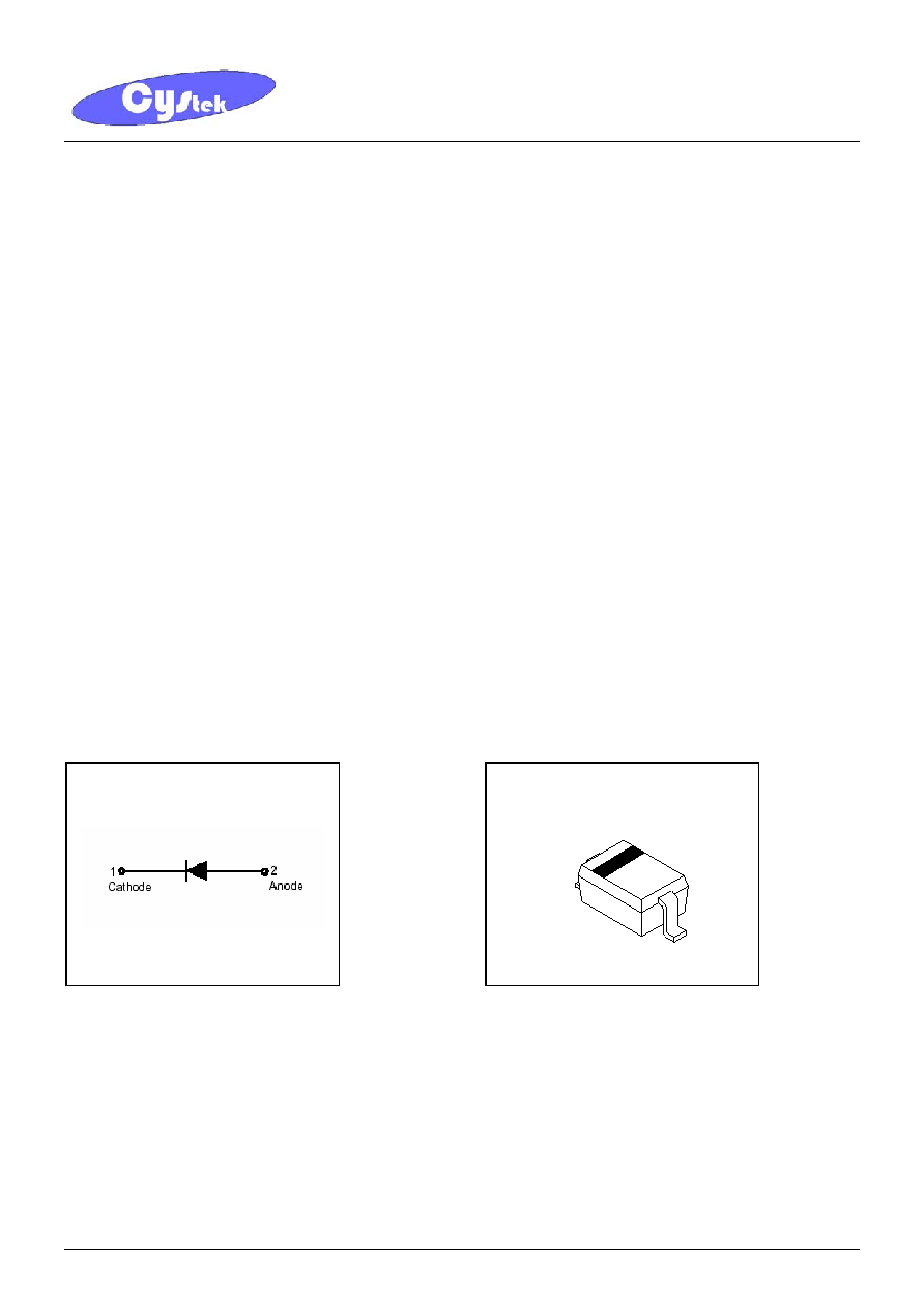
Symbol Outline
SOD-323
BAT54S2
CYStech Electronics Corp.
Spec. No. : C302S
Issued Date : 2004.11.26
Revised Date :
Page No. : 2/4
BAT54S2
CYStek Product Specification
Absolute Maximum Ratings
Symbol Parameter
Conditions
Min Max Unit
V
R
continuous
reverse
voltage
- 30
V
I
F
continuous forward current
-
200
mA
I
FRM
repetitive peak forward current
tp1s, 0.5 -
300
mA
I
FSM
non-repetitive peak forward current
tp<10ms
-
600
mA
Ptot
total power dissipation
Tamb25
- 200
mW
Tstg storage
temperature
-65
+150
Tj junction
temperature
-
125
Tamb
operating ambient temperature
-65
+125
Characteristics
(Ta=25
°
C, unless otherwise specified)
Parameter Symbol Condition
Min.
Max.
Unit
Reverse Breakdown Voltage
V
BR
I
R
=100µA 30
-
V
V
F
(1) I
F
=0.1mA -
240
mV
V
F
(2) I
F
=1mA -
320
mV
V
F
(3) I
F
=10mA -
400
mV
V
F
(4) I
F
=30mA -
500
mV
Forward Voltage (
Note 1
)
V
F
(5) I
F
=100mA -
800
mV
Reverse Leakage Current (
Note 2
) I
R
V
R
=25V
-
2
µA
Diode Capacitance
C
D
V
R
=1V, f=1MHz
-
10
pF
Reverse Recovery Time
trr
when switched from I
F
= 10mA
to I
R
=10mA; R
L
=100
;
measured at I
R
=1mA
- 5 ns
Notes
:
1.pulse test, tp=380µs, duty cycle<2%.
2.pulse test, tp=300µs, duty cycle<2%.
Thermal Characteristics
Symbol Parameter
Conditions
Value Unit
R
th j-a
thermal resistance from junction to ambient
note 1
635
K/W
Note 1 : Device mounted on a FR-4 PCB
CYStech Electronics Corp.
Spec. No. : C302S
Issued Date : 2004.11.26
Revised Date :
Page No. : 3/4
BAT54S2
CYStek Product Specification
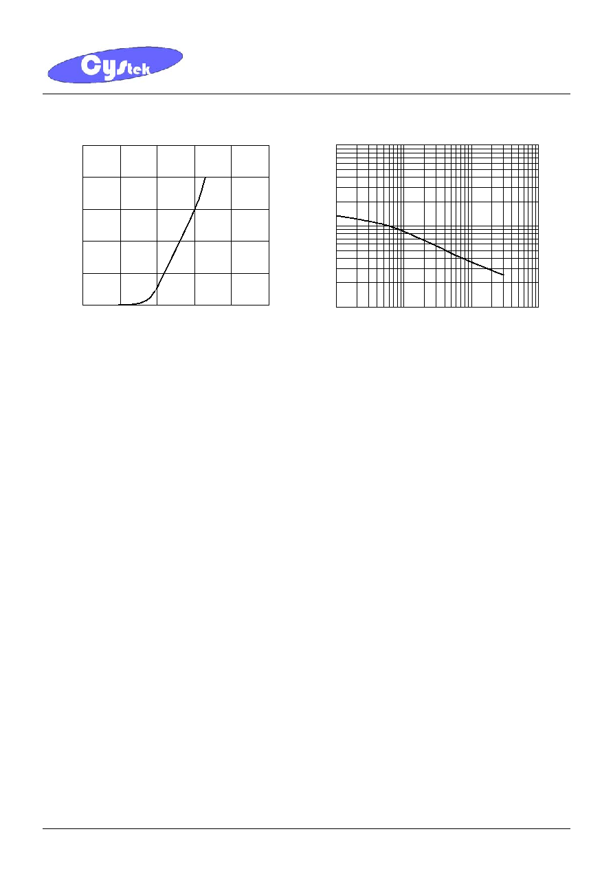
Characteristic Curves
Forward Current & Forward Voltage
0
50
100
150
200
250
0
200
400
600
800
1000
Forward Voltage-V
F
(mV)
F
o
r
w
ar
d C
u
r
r
en
t
-
I
F
(m
A
)
Diode Capacitance & Reverse-Biased Voltage
1
10
100
0.1
1
10
100
Reverse Biased Voltage-V
R
(V)
D
i
ode C
a
p
a
c
i
t
anc
e-
C
d
(
p
F
)

CYStech Electronics Corp.
Spec. No. : C302S
Issued Date : 2004.11.26
Revised Date :
Page No. : 4/4
BAT54S2
CYStek Product Specification
SOD-323 Dimension
*: Typical
Inches Millimeters
Inches Millimeters
DIM
Min. Max. Min. Max.
DIM
Min. Max. Min. Max.
A 0.0630
0.0709 1.60 1.80 E
0.0060 REF
0.15 REF
B 0.0453
0.0531 1.15 1.35 H 0.0000
0.0040 0.00 0.10
C 0.0315
0.0394 0.80 1.00 J 0.0035
0.0070 0.089 0.177
D 0.0098
0.0157 0.25 0.40 K 0.0906
0.1063 2.30 2.70
Notes:
1.Controlling dimension : millimeters.
2.Lead thickness specified per L/F drawing with solder plating.
3.If there is any question with packing specification or packing method, please contact your local CYStek sales office.
Material:
·
Lead: 42 Alloy ; solder plating
·
Mold Compound: Epoxy resin family, flammability solid burning class: UL94V-0
Important Notice:
·
All rights are reserved. Reproduction in whole or in part is prohibited without the prior written approval of CYStek.
·
CYStek reserves the right to make changes to its products without notice.
·
CYStek semiconductor products are not warranted to be suitable for use in Life-Support Applications, or systems.
·
CYStek assumes no liability for any consequence of customer product design, infringement of patents, or application assistance.
D
A
H
J
K
C
E
B
1
2
Style: Pin 1.Cathode 2.Anode
2-Lead SOD-323 Plastic Surface
Mounted Package,
CYStek Package Code: S2
Marking:
5 H
JV