CPLDs Designed for Migration
Quantum38KTM ISRTM
CPLD Family
PRELIMINARY
Cypress Semiconductor Corporation
·
3901 North First Street
·
San Jose
·
CA 95134
·
408-943-2600
Document #: 38-03043 Rev. *D
Revised April 17, 2002
Features
· High density
-- 30K to 100K usable gates
-- 512 to 1536 macrocells
-- 136 to 302 maximum I/O pins
-- Eight Dedicated Inputs including four clock pins and
four global I/O control signal pins; four JTAG inter-
face pins for reconfigurability/boundary scan
· Embedded Memory
-- 16 Kb to 48 Kb embedded dual-port Channel memory
· 125 MHz in-system operation
· AnyVoltTM
interface
-- 3.3V and 2.5V V
CC
operation
-- 3.3V, 2.5V and 1.8V I/O capability
· Low Power Operation
-- 0.18-
µ
m 6-layer metal SRAM-based logic process
-- Full-CMOS implementation of product term array
· Simple timing model
-- No penalty for using full 16 product terms / macrocell
-- No delay for single product term steering or sharing
· Flexible clocking
-- Four synchronous clocks per device
-- Locally generated Product Term clock
-- Clock polarity control at each register
· Carry-chain logic for fast and efficient arithmetic oper-
ations
· Multiple I/O standards supported:
-- LVCMOS (3.3/3.0/2.5/1.8V), LVTTL, 3.3V PCI
· Compatible with NOBLTM, ZBTTM, and QDRTM SRAMs
· Programmable slew rate control on each I/O pin
· User-Programmable Bus Hold capability on each I/O pin
· Fully PCI compliant (as per PCI spec rev. 2.2)
· Compact PCI hot swap ready
· Multiple package/pinout offering across all densities
-- 208 to 484 pins in PQFP and FBGA packages
-- Simplifies design migration across density
· In-System ReprogrammableTM (ISRTM)
-- JTAG-compliant on-board configuration
-- Design changes don't cause pinout changes
· IEEE1149.1 JTAG boundary scan
· Pin-to-pin compatible with Cypress's high-end
Delta39KTM CPLDs allowing easy migration path to:
-- More embedded memory
-- Spread AwareTM PLL
-- Higher density and higher speed devices
-- High speed I/O standards and more....
Development Software
· Warp
®
-- IEEE 1076/1164 VHDL or IEEE 1364 Verilog context
sensitive editing
-- Active-HDL FSM graphical finite state machine editor
-- Active-HDL SIM post-synthesis timing simulator
-- Architecture Explorer for detailed design analysis
-- Static Timing Analyzer for critical path analysis
-- Available on, Windows 98TM, Windows NTTM, Win-
dows METM, Windows 2000TM, and Sun Solaris 2.5 &
later for $99
-- Supports all Cypress programmable logic products
Notes:
1.
Upper limit of typical gates is calculated by assuming only 50% of the channel memory is used.
2.
Standby I
CC
values are with no output load and stable inputs.
Quantum38KTM ISR CPLD Family Members
Device
Typical Gates
[1]
Macrocells
Channel
memory
(Kb)
Maximum
I/O Pins
f
MAX2
(MHz)
Speed -- t
PD
Pin-to-Pin
(ns)
Standby I
CC
[2]
T
A
=25
°
C
3.3/2.5V
38K30
16K48K
512
16
176
125
10
5 mA
38K50
23K72K
768
24
218
125
10
5 mA
38K100
46K144K
1536
48
302
125
10
10 mA
PRELIMINARY
Quantum38KTM ISRTM
CPLD Family
Document #: 38-03043 Rev. *D
Page 2 of 50
Quantum38K Speed Bins
[3]
Device
125
83
38K30
X
X
38K50
X
X
38K100
X
X
Device Package Offering and I/O Count Including Dedicated Clock and Control Inputs
Device
208-EQFP
28x28 mm
0.5-mm pitch
256-FBGA
17x17 mm
1.0-mm pitch
484-FBGA
23x23 mm
1.0-mm pitch
38K30
136
174
38K50
136
180
218
38K100
136
180
302
Note:
3.
Speed bins shown here are for Commercial operating ranges. Please refer to the Quantum38K Part Numbers (Ordering Information) on page 26 for Industrial-
range speed bins

PRELIMINARY
Quantum38KTM ISRTM
CPLD Family
Document #: 38-03043 Rev. *D
Page 3 of 50
Figure 1. Quantum38K100 Block Diagram (3 Rows x 4 Columns) with I/O Bank Structure
4
GCLK[3:0]
4
4
4
Channel
RAM
4
GCLK[3:0]
4
4
4
4
GCLK[3:0]
4
4
4
4
4
GCLK[3:0]
GCTL[3:0]
I/O Bank 6
I/O Bank 7
I/O Bank 3
I/O Bank 2
I/
O
B
a
n
k
4
I/O
B
a
n
k
5
I/
O
Ba
n
k
1
I/
O
Ba
n
k
0
LB 4
LB 3
LB 0
LB 5
LB 6
LB 7
LB 2
LB 1
PIM
Channel
RAM
Channel
RAM
Channel
RAM
Channel
RAM
Channel
RAM
Channel
RAM
Channel
RAM
Channel
RAM
Channel
RAM
Channel
RAM
Channel
RAM
LB 4
LB 3
LB 0
LB 5
LB 6
LB 7
LB 2
LB 1
PIM
LB 4
LB 3
LB 0
LB 5
LB 6
LB 7
LB 2
LB 1
PIM
LB 4
LB 3
LB 0
LB 5
LB 6
LB 7
LB 2
LB 1
PIM
LB 4
LB 3
LB 0
LB 5
LB 6
LB 7
LB 2
LB 1
PIM
LB 4
LB 3
LB 0
LB 5
LB 6
LB 7
LB 2
LB 1
PIM
LB 4
LB 3
LB 0
LB 5
LB 6
LB 7
LB 2
LB 1
PIM
LB 4
LB 3
LB 0
LB 5
LB 6
LB 7
LB 2
LB 1
PIM
LB 4
LB 3
LB 0
LB 5
LB 6
LB 7
LB 2
LB 1
PIM
LB 4
LB 3
LB 0
LB 5
LB 6
LB 7
LB 2
LB 1
PIM
LB 4
LB 3
LB 0
LB 5
LB 6
LB 7
LB 2
LB 1
PIM
LB 4
LB 3
LB 0
LB 5
LB 6
LB 7
LB 2
LB 1
PIM

PRELIMINARY
Quantum38KTM ISRTM
CPLD Family
Document #: 38-03043 Rev. *D
Page 4 of 50
General Description
The Quantum38K family, based on a 0.18-
µ
m, 6-layer metal
CMOS logic process, offers a wide range of solutions at very
high system performance. With devices ranging from 512 to
1536 macrocells, Quantum38K is the highest density CPLD in
the market besides Cypress's Delta39K. Specifically designed
to address high-volume communication applications, this fam-
ily also integrates Cypress's dual-port memory technology
onto a CPLD.
The architecture is based on Logic Block Clusters (LBC) that
are connected by Horizontal and Vertical (H&V) routing chan-
nels. Each LBC features eight individual Logic Blocks (LB).
Adjacent to each LBC is a channel memory block, which can
be accessed directly from the I/O pins. These channel memory
blocks are highly configurable and can be cascaded in width
and depth. See Figure 1 for a block diagram of the
Quantum38K architecture.
All the members of the Quantum38K family have Cypress's
highly regarded In-System Reprogrammability (ISR) feature,
which simplifies both design and manufacturing flows, thereby
reducing costs. The ISR feature provides the ability to recon-
figure the devices without having design changes cause pinout
or timing changes in most cases. The Cypress ISR function is
implemented through a JTAG-compliant serial interface. Data
is shifted in and out through the TDI and TDO pins respectively.
Superior routability, simple timing, and the ISR allows users to
change existing logic designs while simultaneously fixing pi-
nout assignments and maintaining system performance.
The entire family features JTAG for ISR and boundary scan,
and is compatible with the PCI Local Bus specification, meet-
ing the electrical and timing requirements. The Quantum38K
family also features user programmable bus-hold and slew rate
control capabilities on each I/O pin.
AnyVolt Interface
All Quantum38K devices feature an on-chip regulator, which
accepts 3.3V or 2.5V on the V
CC
supply pins and steps it down
to 1.8V internally, the voltage level at which the core operates.
With Quantum38K's AnyVolt technology, the I/O pins can be
connected to either 1.8V 2.5V, or 3.3V. All Quantum38K devic-
es are 3.3V tolerant regardless of V
CCIO
or V
CC
settings.
Global Routing Description
The routing architecture of the Quantum38K is made up of
horizontal and vertical (H&V) routing channels. These routing
channels allow signals from each of the Quantum38K archi-
tectural components to communicate with one another. In ad-
dition to the horizontal and vertical routing channels that inter-
connect the I/O banks, channel memory blocks, and logic
block clusters, each LBC contains a Programmable Intercon-
nect Matrix (PIMTM), which is used to route signals among the
logic blocks.
Figure 2 is a block diagram of the routing channels that inter-
face within the Quantum38K architecture. The LBC is exactly
the same for every member of the Quantum38K CPLD family.
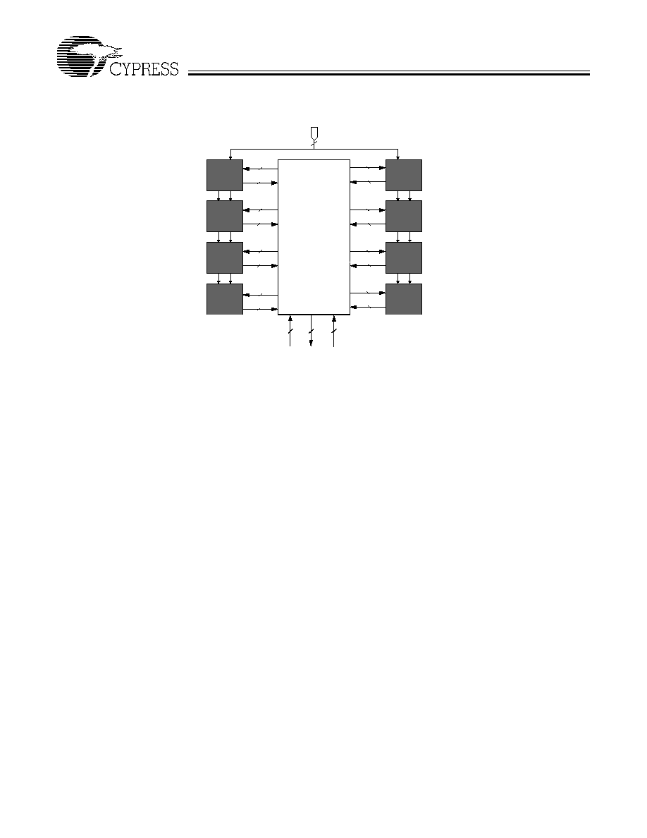
Logic Block Cluster (LBC)
The Quantum38K architecture consists of several logic block
clusters, each of which have 8 Logic Blocks (LB) connected via
a Programmable Interconnect Matrix (PIM) as shown in Figure
3. All LBCs interface with each other via horizontal and vertical
routing channels.
Device
V
CC
V
CCIO
38K
3.3V or 2.5V
3.3V or 2.5V or 1.8V
Figure 2. Quantum38K Routing Interface
LB
Cluster
PIM
Cluster
Memory
Block
LB
LB
LB
LB
Cluster
Memory
Block
LB
LB
LB
Channel
Memory
Block
I/O Block
I/O B
l
ock
Channel memory
outputs drive
dedicated tracks in the
horizontal and vertical
routing channels
H-to-V
PIM
V-to-H
PIM
Pin inputs from the I/O cells
drive dedicated tracks in the
horizontal and vertical routing
channels
72
72
64
64
LB
LB
LB
LB
LB
LB
LB
LB
PRELIMINARY
Quantum38KTM ISRTM
CPLD Family
Document #: 38-03043 Rev. *D
Page 5 of 50
Logic Block (LB)
The logic block is the basic building block of the Quantum38K
architecture. It consists of a product term array, an intelligent
product-term allocator, and 16 macrocells.
Product Term Array
Each logic block features a 72 x 83 programmable product
term array. This array accepts 36 inputs from the PIM. These
inputs originate from device pins and macrocell feedbacks as
well as channel memory feedbacks. Active LOW and active
HIGH versions of each of these inputs are generated to create
the full 72-input field. The 83 product terms in the array can be
created from any of the 72 inputs.
Of the 83 product terms, 80 are for general-purpose use for the
16 macrocells in the logic block. Two of the remaining three
product terms in the logic block are used as asynchronous set
and asynchronous reset product terms. The final product term
is the Product Term clock (PTCLK) and is shared by all 16
macrocells within a logic block.
Product Term Allocator
Through the product term allocator, Warp software automati-
cally distributes the 80 product terms as needed among the 16
macrocells in the logic block. The product term allocator pro-
vides two important capabilities without affecting performance:
product term steering and product term sharing.
Product Term Steering
Product term steering is the process of assigning product
terms to macrocells as needed. For example, if one macrocell
requires ten product terms while another needs just three, the
product term allocator will "steer" ten product terms to one
macrocell and three to the other. On Quantum38K devices,
product terms are steered on an individual basis. Any number
between 1and 16 product terms can be steered to any macro-
cell.
Product Term Sharing
Product term sharing is the process of using the same product
term among multiple macrocells. For example, if more than
one function has one or more product terms in its equation that
are common to other functions, those product terms are only
programmed once. The Quantum38K product term allocator
allows sharing across groups of four macrocells in a variable
fashion. The software automatically takes advantage of this
capability so that the user does not have to intervene.
Note that neither product term sharing nor product term steer-
ing have any effect on the speed of the product. All steering
and sharing configurations have been incorporated in the tim-
ing specifications for the Quantum38K devices.
Figure 3. Quantum38K Logic Block Cluster Diagram
Logic
Block
0
Logic
Block
1
Logic
Block
3
Logic
Block
2
Cluster
Memory
0
PIM
Logic
Block
7
Logic
Block
6
Logic
Block
4
Logic
Block
5
Cluster
Memory
1
64 Inputs From
Horizontal Routing
Channel
64 Inputs From
Vertical Routing
Channel
Clock Inputs
GCLK[3:0]
CC
CC
CC
CC
CC
CC
CC = Carry Chain
16
36
16
36
16
36
16
36
16
36
16
36
16
36
8
25
8
25
4
16
36
64 Inputs from
Horizontal Routing
Channel
144 Outputs to
Horizontal and Vertical
Cluster-to-Channel PIMs
64 Inputs from
Vertical Routing
Channel
16