256K x 18/128K x 36 Synchronous-Pipelined
Cache RAM
CY7C1347C/GVT71128DA36
CY7C1327C/GVT71256DA18
Cypress Semiconductor Corporation
À
3901 North First Street
À
San Jose
À
CA 95134
À
408-943-2600
July 21, 2000
Features
À Fast access times: 2.5 and 3.5 ns
À Fast clock speed: 250, 225, 200, and 166 MHz
À 1-ns set-up time and hold time
À Fast OE access times: 2.5 ns and 3.5 ns
À Optimal for depth expansion (one cycle chip deselect
to eliminate bus contention)
À 3.3V ¡5% and +10% power supply
À 3.3V or 2.5V I/O supply
À 5V tolerant inputs except I/Os
À Clamp diodes to V
SS
at all inputs and outputs
À Common data inputs and data outputs
À Byte Write Enable and Global Write control
À Three chip enables for depth expansion and address
pipeline
À Address, data, and control registers
À Internally self-timed Write Cycle
À Burst control pins (interleaved or linear burst se-
quence)
À Automatic power-down for portable applications
À JTAG boundary scan
À JEDEC standard pinout
À Low profile 119-lead, 14-mm x 22-mm BGA (Ball Grid
Array) and 100-pin TQFP packages
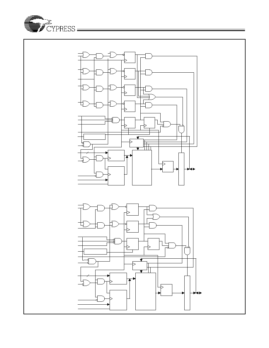
Functional Description
The Cypress Synchronous Burst SRAM family employs
high-speed, low-power CMOS designs using advanced tri-
ple-layer polysilicon, double-layer metal technology. Each
memory cell consists of four transistors and two high-valued
resistors.
The CY7C1347C/GVT71128DA36 and CYC7C1327C/
GVT71256DA18 SRAMs integrate 131,072x36 and
262,144x18 SRAM cells with advanced synchronous periph-
eral circuitry and a 2-bit counter for internal burst operation. All
synchronous inputs are gated by registers controlled by a pos-
itive-edge-triggered clock input (CLK). The synchronous in-
puts include all addresses, all data inputs, address-pipelining
Chip Enable (CE), depth-expansion Chip Enables (CE2 and
CE2), Burst Control Inputs (ADSC, ADSP, and ADV), Write
Enables (BWa, BWb, BWc, BWd, and BWE), and Global Write
(GW).
Asynchronous inputs include the Output Enable (OE) and
Burst Mode Control (MODE). The data outputs (Q), enabled
by OE, are also asynchronous.
Addresses and chip enables are registered with either Ad-
dress Status Processor (ADSP) or Address Status Controller
(ADSC) input pins. Subsequent burst addresses can be inter-
nally generated as controlled by the Burst Advance pin (ADV).
Address, data inputs, and write controls are registered on-chip
to initiate self-timed Write cycle. Write cycles can be one to
four bytes wide as controlled by the write control inputs. Indi-
vidual byte write allows individual byte to be written. BWa con-
trols DQa. BWb controls DQb. BWc controls DQc. BWd con-
trols DQd. BWa, BWb, BWc, and BWd can be active only with
BWE being LOW. GW being LOW causes all bytes to be writ-
ten. The x18 version only has 18 data inputs/outputs (DQa and
DQb) along with BWa and BWb (no BWc, BWd, DQc, and
DQd).
Four pins are used to implement JTAG test capabilities: Test
Mode Select (TMS), Test Data-in (TDI), Test Clock (TCK), and
Test Data-out (TDO). The JTAG circuitry is used to serially shift
data to and from the device. JTAG inputs use LVTTL/LVCMOS
levels to shift data during this testing mode of operation.
The CY7C1347C/GVT71128DA36 and CY7C1327C/
GVT71256DA18 operate from a +3.3V power supply. All inputs
and outputs are LVTTL compatible
Selection Guide
7C1347C-250
71128DA36-4
7C1327C-250
71256DA18-4
7C1347C-225
71128DA36-4.4
7C1327C-225
71256DA18-4.4
7C1347C-200
71128DA36-5
7C1327C-200
71256DA18-5
7C1347C-166
71128DA36-6
7C1327C-166
71256DA18-6
Maximum Access Time (ns)
2.5
2.5
2.5
3.5
Maximum Operating Current (mA)
450
400
360
300
Maximum CMOS Standby Current (mA)
10
10
10
10

CY7C1347C/GVT71128DA36
CY7C1327C/GVT71256DA18
5
128K X 36 Pin Descriptions
X36 BGA Pins
X36 QFP Pins
Name
Type
Description
4P
4N
2A, 3A, 5A, 6A,
3B, 5B, 2C, 3C,
5C, 6C, 2R, 6R,
3T, 4T, 5T
37
36
35, 34, 33, 32,
100, 99, 82, 81,
44, 45, 46, 47,
48, 49, 50
A0
A1
A
Input-
Synchronous
Addresses: These inputs are registered and must meet the
set-up and hold times around the rising edge of CLK. The burst
counter generates internal addresses associated with A0 and
A1, during burst cycle and wait cycle.
5L
5G
3G
3L
93
94
95
96
BWa
BWb
BWc
BWd
Input-
Synchronous
Byte Write: A byte write is LOW for a Write cycle and HIGH for
a Read cycle. BWa controls DQa. BWb controls DQb. BWc
controls DQc. BWd controls DQd. Data I/O are high impedance
if either of these inputs are LOW, conditioned by BWE being
LOW.
4M
87
BWE
Input-
Synchronous
Write Enable: This active LOW input gates byte write opera-
tions and must meet the set-up and hold times around the
rising edge of CLK.
4H
88
GW
Input-
Synchronous
Global Write: This active LOW input allows a full 36-bit Write
to occur independent of the BWE and BWn lines and must
meet the set-up and hold times around the rising edge of CLK.
4K
89
CLK
Input-
Synchronous
Clock: This signal registers the addresses, data, chip enables,
write control and burst control inputs on its rising edge. All
synchronous inputs must meet set-up and hold times around
the clock's rising edge.
4E
98
CE
Input-
Synchronous
Chip Enable: This active LOW input is used to enable the
device and to gate ADSP.
6B
92
CE2
Input-
Synchronous
Chip Enable: This active LOW input is used to enable the
device.
2U
3U
4U
38
39
43
TMS
TDI
TCK
Input
IEEE 1149.1 test inputs. LVTTL-level inputs.
5U
42
TDO
Output
IEEE 1149.1 test output. LVTTL-level output.
1B, 7B, 1C, 7C,
4D, 3J, 5J, 4L,
1R, 5R, 7R, 1T,
2T, 6T, 6U
14, 16, 66
NC
-
No Connect: These signals are not internally connected.
256K X 18 Pin Descriptions
X18 BGA Pins
X18 QFP Pins
Name
Type
Description
4P
4N
2A, 3A, 5A, 6A,
3B, 5B, 2C, 3C,
5C, 6C, 2R, 6R,
2T, 3T, 5T, 6T
37
36
35, 34, 33, 32,
100, 99, 82, 81,
80, 48, 47, 46,
45, 44, 49, 50
A0
A1
A
Input-
Synchronous
Addresses: These inputs are registered and must meet the
set-up and hold times around the rising edge of CLK. The burst
counter generates internal addresses associated with A0 and
A1, during burst cycle and wait cycle.
5L
3G
93
94
BWa
BWb
Input-
Synchronous
Byte Write Enables: A byte write enable is LOW for a Write
cycle and HIGH for a Read cycle. BWa controls DQa. BWb
controls DQb. Data I/O are high impedance if either of these
inputs are LOW, conditioned by BWE being LOW.
4M
87
BWE
Input-
Synchronous
Write Enable: This active LOW input gates byte write opera-
tions and must meet the setup and hold times around the rising
edge of CLK.