2K x 8 Reprogrammable Registered PROM
CY7C245A
Cypress Semiconductor Corporation
·
3901 North First Street
·
San Jose
,
CA 95134
·
408-943-2600
Document #: 38-04007 Rev. *D
Revised November 4, 2003
Features
· Windowed for reprogrammability
· CMOS for optimum speed/power
· High speed
-- 15-ns address set-up
-- 10-ns clock to output
· Low power
-- 330 mW (commercial) for -25 ns
-- 660 mW (military)
· Programmable synchronous or asynchronous output
enable
· On-chip edge-triggered registers
· Programmable asynchronous register (INIT)
· EPROM technology, 100% programmable
· Slim, 300-mil, 24-pin plastic or hermetic DIP
· 5V
±
10% V
CC
, commercial and military
· TTL-compatible I/O
· Direct replacement for bipolar PROMs
· Capable of withstanding greater than 2001V static
discharge
Functional Description
The CY7C245A is a high-performance, 2K x 8, electrically
programmable, read-only memory packaged in a slim 300-mil
plastic or hermetic DIP. The ceramic package may be
equipped with an erasure window; when exposed to UV light
the PROM is erased and can then be reprogrammed. The
memory cells utilize proven EPROM floating-gate technology
and byte-wide intelligent programming algorithms.
The CY7C245A replaces bipolar devices and offers the advan-
tages of lower power, reprogrammability, superior perfor-
mance and high programming yield. The EPROM cell requires
only 12.5V for the supervoltage, and low current requirements
allow gang programming. The EPROM cells allow each
memory location to be tested 100%, because each location is
written into, erased, and repeatedly exercised prior to encap-
sulation. Each PROM is also tested for AC performance to
guarantee that after customer programming the product will
meet AC specification limits.
The CY7C245A has an asynchronous initialize function (INIT).
This function acts as a 2049th 8-bit word loaded into the
on-chip register. It is user programmable with any desired
word, or may be used as a PRESET or CLEAR function on the
outputs. INIT is triggered by a low level, not an edge.
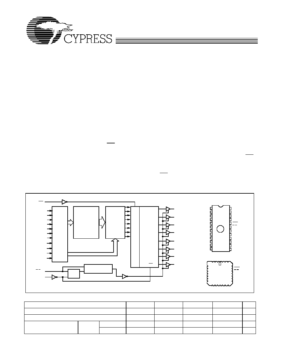
Logic Block Diagram
Pin Configurations
1
2
3
4
5
6
7
8
9
10
11
12
16
17
18
19
20
24
23
22
21
13
14
A
7
A
6
A
5
A
4
A
3
A
2
A
1
A
0
O
0
O
1
O
2
GND
V
CC
A
8
A
9
INIT
CP
O
7
O
6
O
4
O
5
O
3
PROGRAMMABLE
ARRAY
MULTIPLEXER
15
8-BIT
EDGE-
REGISTER
TRIGGERED
O
7
O
6
O
5
O
4
O
3
O
2
O
1
O
0
CP
CP
E/E
S
E/E
S
28
4
5
6
7
8
9
10
3 2 1
27
1314151617
26
25
24
23
22
21
20
11
12
19
A
5
V CC
GND
A
6
A
7
O
3
O
1
O
0
18
O
4
O
5
NC
A
0
A
4
A
3
A
10
NC
NC
NC
INIT
E/E
S
O
7
O
6
A
2
A
1
CP
O
2
A
8
INIT
INIT
IA
LIZ
E
W
O
RD
PRO
G
R
AM
M
A
BL
E
A
9
PROGRAMMABLE
MULTIPLEXER
D
Q
C
A
10
ADDRESS
DECODER
A
0
A
1
A
2
A
3
A
4
A
5
A
6
A
8
A
9
A
10
A
7
COLUMN
ADDRESS
ROW
ADDRESS
DIP Top View
LCC/PLCC (Opaque only) Top View
Selection Guide
7C245A-15
7C245A-18
7C245A-25
7C245A-35
Unit
Minimum Address Set-up Time
15
18
25
35
ns
Maximum Clock to Output
10
12
12
15
ns
Maximum Operating Current Standard
Commercial
120
120
90
90
mA
Military
120
120
120
mA
CY7C245A
Document #: 38-04007 Rev. *D
Page 2 of 12
Operating Modes
The CY7C245A is a CMOS electrically programmable read
only memory organized as 2048 words x 8 bits and is a
pin-for-pin replacement for bipolar TTL fusible link PROMs.
The CY7C245A incorporates a D-type, master-slave register
on chip, reducing the cost and size of pipelined micropro-
grammed systems and applications where accessed PROM
data is stored temporarily in a register. Additional flexibility is
provided with a programmable synchronous (E
S
) or
asynchronous (E) output enable and asynchronous initial-
ization (INIT).
Upon power-up the state of the outputs will depend on the
programmed state of the enable function (E
S
or E). If the
synchronous enable (E
S
) has been programmed, the register
will be in the set condition causing the outputs (O0O7) to be
in the OFF or high-impedance state. If the asynchronous
enable (E) is being used, the outputs will come up in the OFF
or high-impedance state only if the enable (E) input is at a
HIGH logic level. Data is read by applying the memory location
to the address inputs (A0A10) and a logic LOW to the enable
input. The stored data is accessed and loaded into the master
flip-flops of the data register during the address set-up time. At
the next LOW-to-HIGH transition of the clock (CP), data is
transferred to the slave flip-flops, which drive the output
buffers, and the accessed data will appear at the outputs
(O0O7).
If the asynchronous enable (E) is being used, the outputs may
be disabled at any time by switching the enable to a logic
HIGH, and may be returned to the active state by switching the
enable to a logic LOW.
If the synchronous enable (E
S
) is being used, the outputs will
go to the OFF or high-impedance state upon the next positive
clock edge after the synchronous enable input is switched to
a HIGH level. If the synchronous enable pin is switched to a
logic LOW, the subsequent positive clock edge will return the
output to the active state. Following a positive clock edge, the
address and synchronous enable inputs are free to change
since no change in the output will occur until the next
low-to-high transition of the clock. This unique feature allows
the CY7C245A decoders and sense amplifiers to access the
next location while previously addressed data remains stable
on the outputs.
System timing is simplified in that the on-chip edge triggered
register allows the PROM clock to be derived directly from the
system clock without introducing race conditions. The on-chip
register timing requirements are similar to those of discrete
registers available in the market.
The CY7C245A has an asynchronous initialize input (INIT).
The initialize function is useful during power-up and time-out
sequences and can facilitate implementation of other sophis-
ticated functions such as a built-in "jump start" address. When
activated, the initialize control input causes the contents of a
user-programmed 2049th 8-bit word to be loaded into the
on-chip register. Each bit is programmable and the initialize
function can be used to load any desired combination of 1s
and 0s into the register. In the unprogrammed state, activating
INIT will generate a register CLEAR (all outputs LOW). If all
the bits of the initialize word are programmed, activating INIT
performs a register PRESET (all outputs HIGH).
Applying a LOW to the INIT input causes an immediate load
of the programmed initialize word into the master and slave
flip-flops of the register, independent of all other inputs,
including the clock (CP). The initialize data will appear at the
device outputs after the outputs are enabled by bringing the
asynchronous enable (E) LOW.
Erasure Characteristics
Wavelengths of light less than 4000 Angstroms begin to erase
the 7C245A. For this reason, an opaque label should be
placed over the window if the PROM is exposed to sunlight or
fluorescent lighting for extended periods of time.
The recommended dose for erasure is ultraviolet light with a
wavelength of 2537 Angstroms for a minimum dose (UV
intensity multiplied by exposure time) of 25 Wsec/cm2. For an
ultraviolet lamp with a 12 mW/cm2 power rating the exposure
time would be approximately 35 minutes. The 7C245A needs
to be within 1 inch of the lamp during erasure. Permanent
damage may result if the PROM is exposed to high-intensity
UV light for an extended period of time. 7258 Wsec/cm2 is the
recommended maximum dosage.
Programming Information
Programming support is available from Cypress as well as
from a number of third-party software vendors. For detailed
programming information, including a listing of software
packages, please see the PROM Programming Information
located at the end of this section. Programming algorithms can
be obtained from any Cypress representative.
Bit Map Data
Programmer Address
RAM Data
Decimal
Hex
Contents
0
0
Data
.
.
.
.
.
.
.
.
.
2047
7FF
Data
2048
800
Init Byte
2049
801
Control Byte
Control Byte
00
Asynchronous output enable (default state)
01
Synchronous output enable
CY7C245A
Document #: 38-04007 Rev. *D
Page 3 of 12
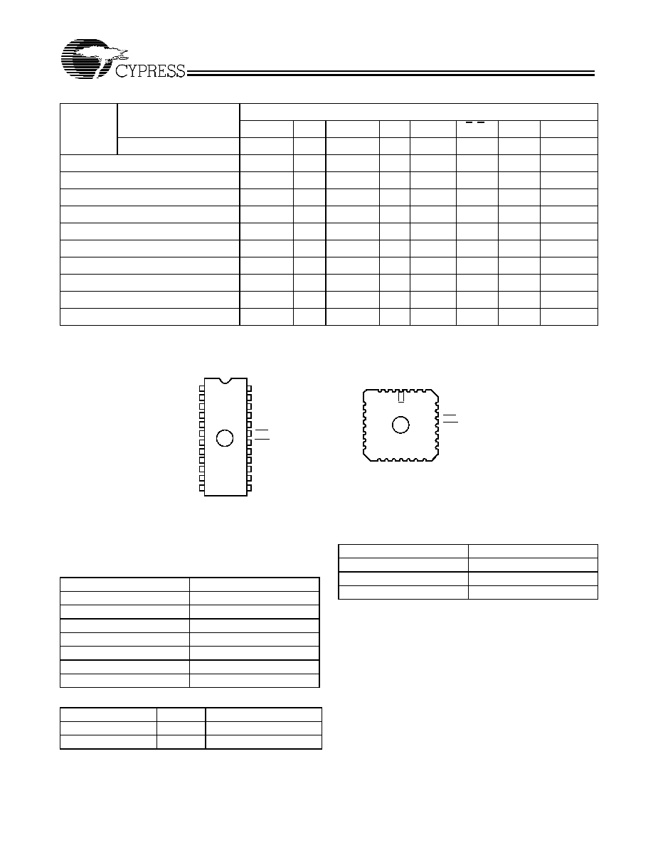
MILITARY SPECIFICATIONS
Group A Subgroup Testing
Note:
1. X = "don't care" but not to exceed V
CC
+ 5%.
Table 1. Mode Selection
Mode
Read or Output Disable
Pin Function
[1]
A
10
A
4
A
3
A
2
A
1
A
0
CP
E, E
S
INIT
O
7
O
0
Other
A
10
A
4
A
3
A
2
A
1
A
0
PGM
VFY
V
PP
D
7
D
0
Read
A
10
A
4
A
3
A
2
A
1
A
0
V
IL
/V
IH
V
IL
V
IH
O
7
O
0
Output Disable
A
10
A
4
A
3
A
2
A
1
A
0
X
V
IH
V
IH
High Z
Initialize
A
10
A
4
A
3
A
2
A
1
A
0
X
V
IL
V
IL
Init. Byte
Program
A
10
A
4
A
3
A
2
A
1
A
0
V
ILP
V
IHP
V
PP
D
7
D
0
Program Verify
A
10
A
4
A
3
A
2
A
1
A
0
V
IHP
V
ILP
V
PP
O
7
O
0
Program Inhibit
A
10
A
4
A
3
A
2
A
1
A
0
V
IHP
V
IHP
V
PP
High Z
Intelligent Program
A
10
A
4
A
3
A
2
A
1
A
0
V
ILP
V
IHP
V
PP
D
7
D
0
Program Synchronous Enable
A
10
A
4
V
IHP
A
2
A
1
V
PP
V
ILP
V
IHP
V
PP
High Z
Program Initialization Byte
A
10
A
4
V
ILP
A
2
A
1
V
PP
V
ILP
V
IHP
V
PP
D
7
D
0
Blank Check Zeros
A
10
A
4
A
3
A
2
A
1
A
0
V
IHP
V
ILP
V
PP
Zeros
1
2
3
4
5
6
7
8
9
10
11
12
16
17
18
19
20
24
23
22
21
13
14
A
8
A
7
A
6
A
5
A
4
A
3
A
2
A
1
A
0
D
0
D
1
D
2
GND
V
CC
D
7
D
6
D
4
D
5
D
3
15
A
9
A
10
V
PP
VFY
PGM
28
4
5
6
7
8
9
10
3 2 1
27
1314151617
26
25
24
23
22
21
20
11
12
19
A
5
V
CC
GND
A
6
A
7
D
3
D
1
D
0
18
D
4
D
5
NC
A
0
A
4
A
3
A
8
NC
NC
D
7
D
6
A
2
A
1
D
2
A
10
V
PP
VFY
PGM
NC
A
9
DIP Top View
LCC/PLCC (Opaque Only) Top View
Figure 1. Programming Pinouts
DC Characteristics
Parameter
Subgroups
V
OH
1, 2, 3
V
OL
1, 2, 3
V
IH
1, 2, 3
V
IL
1, 2, 3
I
IX
1, 2, 3
I
OZ
1, 2, 3
I
CC
1, 2, 3
SMD Cross Reference
SMD Number
Suffix
Cypress Number
5962-88735
033X
CY7C245A-25LMB
5962-88735
04LX
CY7C245A-25DMB
Switching Characteristics
Parameter
Subgroups
t
SA
7, 8, 9, 10, 11
t
HA
7, 8, 9, 10, 11
t
CO
7, 8, 9, 10, 11
CY7C245A
Document #: 38-04007 Rev. *D
Page 4 of 12
Maximum Ratings
[2]
(Above which the useful life may be impaired. For user guide-
lines, not tested.)
Storage Temperature
..................................... -
65°C to +150°C
Ambient Temperature with
Power Applied
.................................................. -
55°C to +125°C
Supply Voltage to Ground Potential
(Pin 24 to Pin 12)
.................................................-
0.5V to +7.0V
DC Voltage Applied to Outputs
in High Z State
.....................................................-
0.5V to +7.0V
DC Input Voltage
.................................................-
3.0V to +7.0V
DC Program Voltage (Pins 7, 18, 20) ........................... 13.0V
UV Erasure ................................................... 7258 Wsec/cm
2
Static Discharge Voltage........................................... > 2001V
(per MIL-STD-883, Method 3015)
Latch-up Current..................................................... > 200 mA
Operating Range
Range
Ambient Temperature
V
CC
Commercial
0°C to +70°C
5V
±
10%
Military
[3]
-
55°C to +125°C
5V
±
10%
Industrial
40°C to +85°C
5V ±10%
Electrical Characteristics
Over the Operating Range
[4,5]
Parameter
Description
Test Conditions
7C245A-15
7C245A-18
7C245A-25
7C245A-35
7C245A-45
Unit
Min.
Max.
Min. Max. Min.
Max.
V
OH
Output HIGH Voltage
V
CC
= Min., I
OH
=
-
4.0 mA
V
IN
= V
IH
or V
IL
2.4
2.4
2.4
V
V
OL
Output LOW Voltage
V
CC
= Min., I
OL
= 16 mA
V
IN
= V
IH
or V
IL
0.4
0.4
0.4
V
V
IH
Input HIGH Level
Guaranteed Input Logical
HIGH Voltage for All Inputs
2.0
V
CC
2.0
V
CC
2.0
V
CC
V
V
IL
Input LOW Level
Guaranteed Input Logical
LOW Voltage for All Inputs
0.8
0.8
0.8
V
I
IX
Input Leakage Current
GND < V
IN
< V
CC
-
10
+10
-
10
+10
-
10
+10
µ
A
V
CD
Input Clamp Diode Voltage
Note 5
I
OZ
Output Leakage Current
GND < V
O
< V
CC
Output
Disabled
[6]
-
10
+10
-
10
+10
-
10
+10
µ
A
I
OS
Output Short Circuit Current
V
CC
= Max., V
OUT
= 0.0V
[7]
-
20
-
90
-
20
-
90
-
20
-
90
mA
I
CC
Power Supply Current
V
CC
= Max.,
I
OUT
= 0 mA
Com'l
120
120
90
mA
Mil
120
120
V
PP
Programming Supply Voltage
12
13
12
13
12
13
V
I
PP
Programming Supply Current
50
50
50
mA
V
IHP
Input HIGH Programming Voltage
3.0
3.0
3.0
V
V
ILP
Input LOW Programming Voltage
0.4
0.4
0.4
V
Capacitance
[5]
Parameter
Description
Test Conditions
Max.
Unit
C
IN
Input Capacitance
T
A
= 25
°
C, f = 1 MHz,
V
CC
= 5.0V
10
pF
C
OUT
Output Capacitance
10
pF
Notes:
2. The voltage on any input or I/O pin cannot exceed the power pin during power-up.
3. T
A
is the "instant on" case temperature.
4. See page 3 of this data sheet for Group A subgroup testing information.
5. See the "Introduction to CMOS PROMs" section of the Cypress Data Book for general information on testing.
6. For devices using the synchronous enable, the device must be clocked after applying these voltages to perform this measurement.
7. For test purposes, not more than one output at a time should be shorted. Short circuit test duration should not exceed 30 seconds.
CY7C245A
Document #: 38-04007 Rev. *D
Page 5 of 12
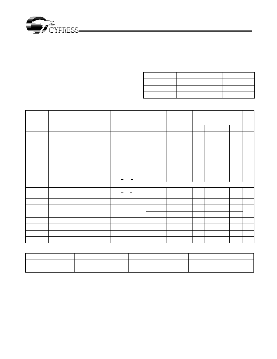
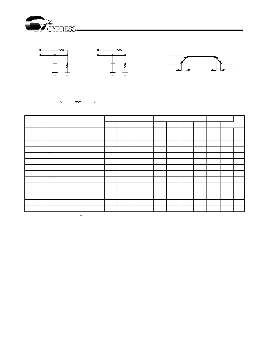
AC Test Loads and Waveforms
[4, 5]
Switching Characteristics
Over Operating Range
[4, 5]
Parameter
Description
7C245A-15
7C245A-18
7C245A-35
7C245A-25
7C245A-35
Unit
Min.
Max.
Min.
Max.
Min.
Max.
Min.
Max.
Min.
Max.
t
SA
Address Set-Up to Clock HIGH
15
18
25
35
45
ns
t
HA
Address Hold from Clock HIGH
0
0
0
0
0
ns
t
CO
Clock HIGH to Valid Output
10
12
12
15
25
ns
t
PWC
Clock Pulse Width
10
12
15
20
20
ns
t
SES
E
S
Set-Up to Clock HIGH
10
10
12
15
15
ns
t
HES
E
S
Hold from Clock HIGH
5
5
5
5
5
ns
t
DI
Delay from INIT to Valid Output
15
20
20
20
35
ns
t
RI
INIT Recovery to Clock HIGH
10
12
15
20
20
ns
t
PWI
INIT Pulse Width
10
12
15
20
25
ns
t
COS
Valid Output from Clock HIGH
[8]
15
15
15
20
30
ns
t
HZC
Inactive Output from Clock
HIGH
[8]
15
15
15
20
30
ns
t
DOE
Valid Output from E LOW
[9]
12
15
15
20
30
ns
t
HZE
Inactive Output from E HIGH
[9]
15
15
15
20
30
ns
Notes:
8. Applies only when the synchronous (E
S
) function is used.
9. Applies only when the asynchronous (E) function is used.
3.0V
5V
OUTPUT
R1 250
R2
167
50 pF
INCLUDING
JIG AND
SCOPE
GND
90%
10%
90%
10%
5 ns
5 ns
5V
OUTPUT
5 pF
INCLUDING
JIG AND
SCOPE
(b) High Z Load
OUTPUT
2.0V
Equivalent to:
TH ÉVENIN EQUIVALENT
100
R1 250
(a) Normal Load
R2
167
ALL INPUT PULSES